

EMI filter and line termination for USB downstream ports
Applications
EMI Filter and line termination for USB
downstream ports on:
■ Desktop computer
■ Notebooks
■ Workstations
■ USB Hubs
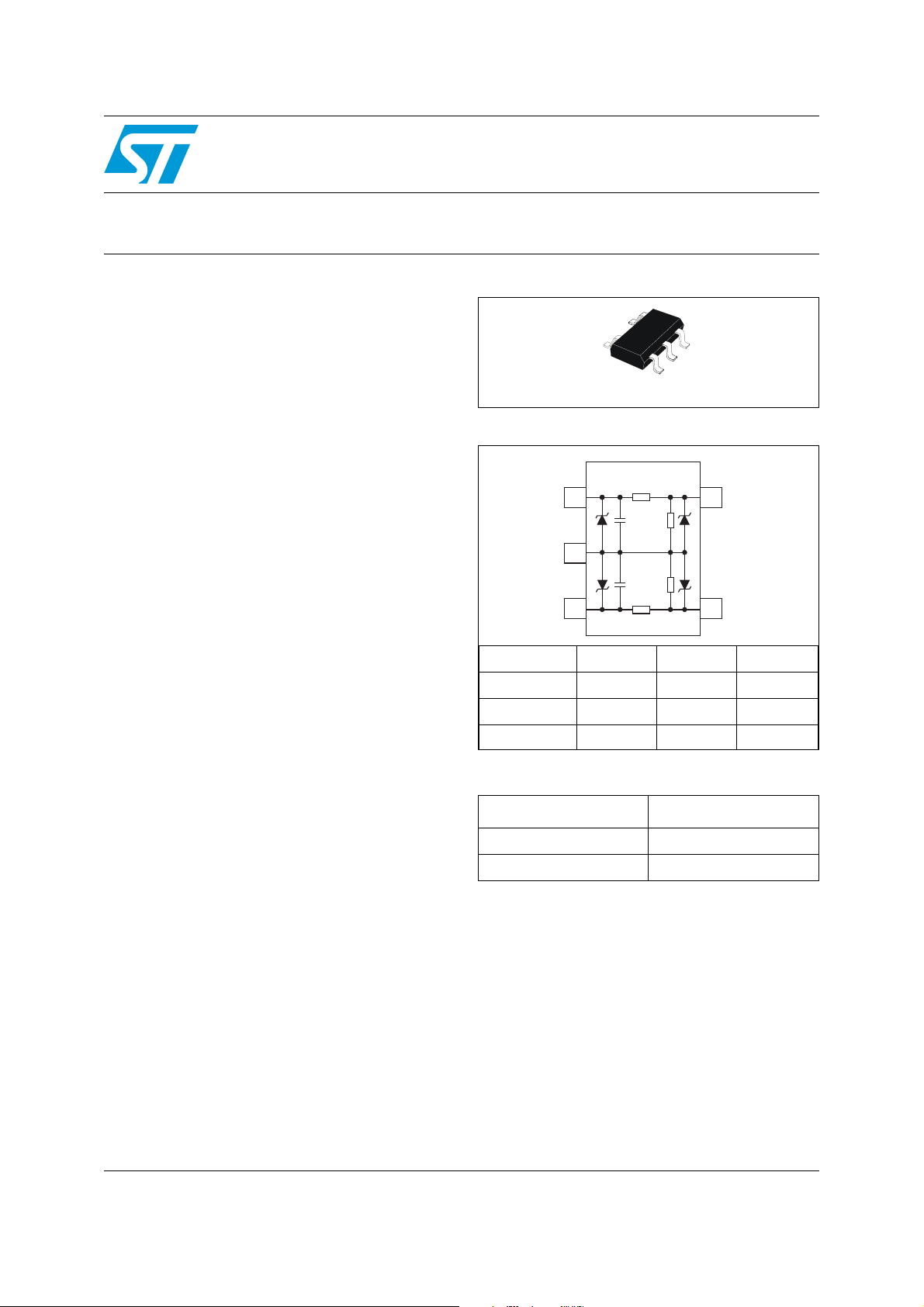
USBDFxxW5
SOT323-5L
Functional diagram
Features
■ Monolithic device with recommended line
termination for USB downstream ports
■ Integrated Rt series termination and Ct
bypassing capacitors.
■ Integrated ESD protection
■ Small package size
Description
The USB specification requires USB downstream
ports to be terminated with pull-down resistors
from the D+ and D- lines to ground. On the
implementation of USB systems, the radiated and
conducted EMI should be kept within the required
levels as stated by the FCC regulations. In
addition to the requirements of termination and
EMC compatibility, the computing devices are
required to be tested for ESD susceptibility.
The USBDFxxW5 provides the recommended line
termination while implementing a low pass filter to
limit EMI levels and providing ESD protection
which exceeds IEC 61000-4-2 level 4 standard.
The device is packaged in a SOT323-5L, which is
a very small (50% smaller than the standard
SOT23).
Complies with the following standards
IEC 61000-4-2, level 4 ±15 kV (air discharge)
±8 kV (contact discharge)
MIL STD 883C, Method 3015-6
Class 3 C = 100 pF R = 1500 W
3 positive strikes and 3 negative strikes (F = 1 Hz)
D+ In
Gnd
D- In
Rt
Ct
Rd
Rd
Ct
Rt
R
t
D+ Out
D- Out
R
d
C
t
USBDF01W5 33 Ω 15 kΩ 47 pF
USBDF02W5 15 Ω 15 kΩ 47 pF
Tolerance ±10% ±10% ±20%
Order codes
Part number Marking
USBDF01W5 UD1
USBDF02W5 UD2
Benefits
■ EMI / RFI noise suppression
■ Required line termination for USB downstream
ports
■ ESD protection exceeding
IEC61000-4-2 level 4
■ IPAD™ technology provides high flexibility in
the design of high density boards
■ Tailored to meet USB 1.1 standard
TM: IPAD is a trademark of STMicroelectronics
September 2006 Rev 3 1/11
www.st.com
11
Characteristics USBDFxxW5
1 Characteristics
Table 1. Absolute maximum ratings (T
Symbol Parameter Value Unit
amb
= 25° C)
V
PP
T
T
stg
T
P
Table 2. Electrical characteristics (T
ESD discharge IEC 61000-4-2, contact discharge
ESD discharge - MIL STD 883 - Method 3015-6
Operating junction temperature range -40 to 150 °C
j
Storage temperature range - 55 to +150 °C
Lead solder temperature (10 second duration) 260 °C
L
Power rating per resistor 100 mW
r
Symbol Parameters Test conditions Min Typ Max Unit
V
BR
V
F
Diode breakdown voltage IR = 1 mA 6 V
Diode forward voltage drop IF = 50 mA 0.9 V
2 Application information
Figure 1. USB Standard requirements
Full-speed or
Low-speed USB
Transceiver
Host or
Hub port
Rt
Ct
Rt
15k
Ct
15k
D+
D-
= 25° C)
amb
Twisted pair shielded
Zo = 90ohms
5m max
D+
D-
+Vbus
1.5k
±15
±25
Rt
Full-speed USB
Ct
Rt
Transceiver
Ct
Hub 0 or
Full-speed function
kV
FULL SPEED CONNECTION
Full-speed or
Low-speed USB
Transceiver
Host or
Hub port
Rt
Ct
Rt
15k
Ct
15k
D+
Untwisted unshielded
D-
LOW SPEED CONNECTION
2/11
3m max
D+
D-
+Vbus
1.5k
Rt
Low-speed USB
Ct
Rt
Transceiver
Ct
Hub 0 or
Low-speed function

USBDFxxW5 Application information
Figure 2. Application example
Upstream portDownstream port
Host/Hub USB
port transceiver
2.1 EMI filtering
Current FCC regulations requires that class B computing devices meet specified maximum
levels for both radiated and conducted EMI.
● Radiated EMI covers the frequency range from 30 MHz to 1 GHz.
● Conducted EMI covers the 450 kHz to 30 MHz range.
For the types of devices utilizing the USB the most difficult test to pass is usually the
radiated EMI test. For this reason the USBDF device aims to minimize radiated EMI.
The differential signal (D+ and D-) of the USB does not contribute significantly to radiated or
conducted EMI because the magnetic field of the two conductors exactly cancels each
other.
D+
USBDF
xxW5
D-
(1) for a low-speed port
(2) for a full-speed port
CABLE
D+ (1)
D- (2)
+Vbus
D- (1)
D+ (2)
USBUF
xxW6
Peripheral
transceiver
The inside of the PC environment is very noisy and designers must minimise noise coupling
from the different sources. D+ and D- must not be routed near high speed lines (clocks...).
Induced common mode noise can be minimised by running pairs of USB signals parallel to
each other and running grounded guard trace on each side of the signal pair from the USB
controller to the USBDF device.
If possible, locate the USBDF device physically near the USB connectors. Distance between
the USB controller and the USB connector must be minimized.
The 47 pF (C
) capacitors are used to divert high frequency energy to ground and for edge
t
control, and must be placed between the USB Controller and the series termination
resistors (R
). Both Ct and Rt should be placed as close to the mSB Controller as
t
practicable.
The USBDFxxW5 ensure a filtering protection against electroMagnetic and radio-frequency
Interference thanks to its low-pass filter structure. This filter is characterized by the following
parameters :
● cut-off frequency
● Insertion loss
● high frequency rejection
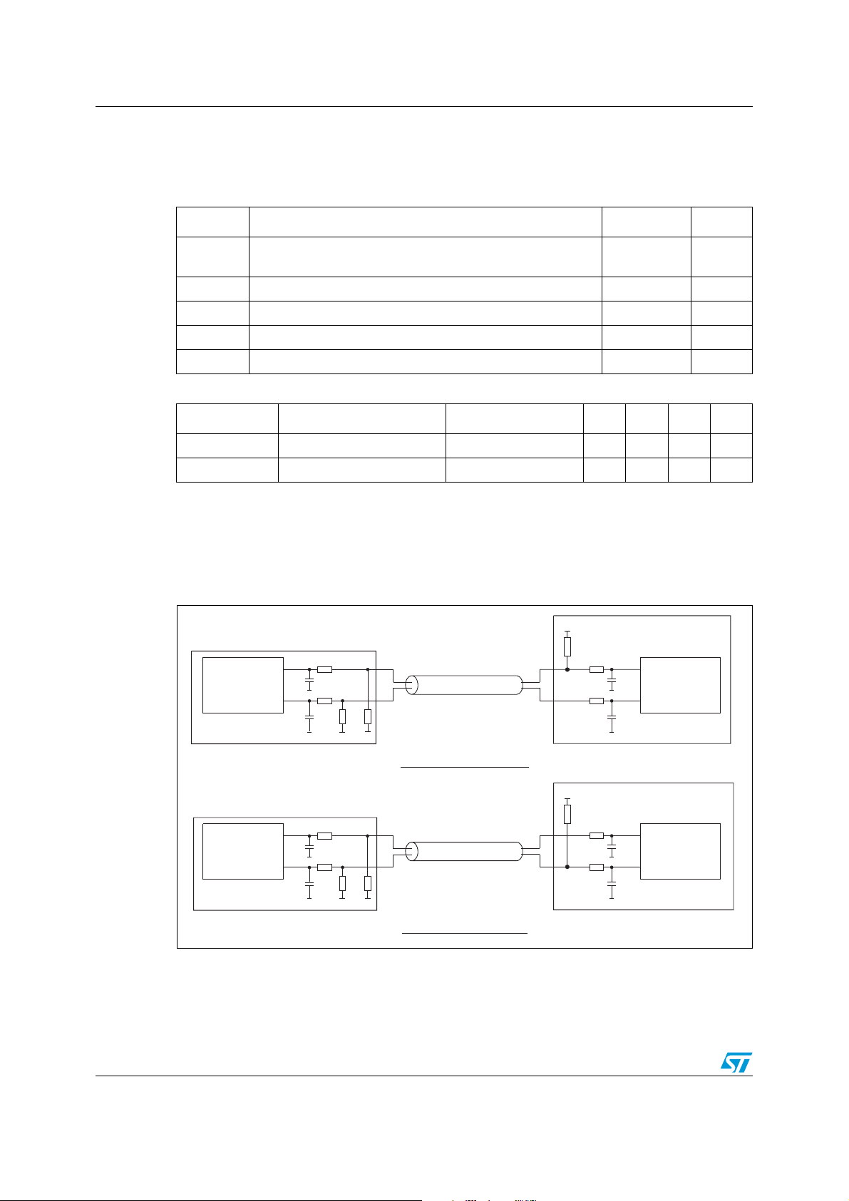
Figure 4. shows the attenuation curve for frequencies up to 3 GHz.
3/11
Application information USBDFxxW5
Figure 3. Measurement configuration Figure 4. USBDFxxW5 attenuation
curve
Insertion loss (dB)
0
TG OUT
50 Ω
Vg
2.2 ESD protection
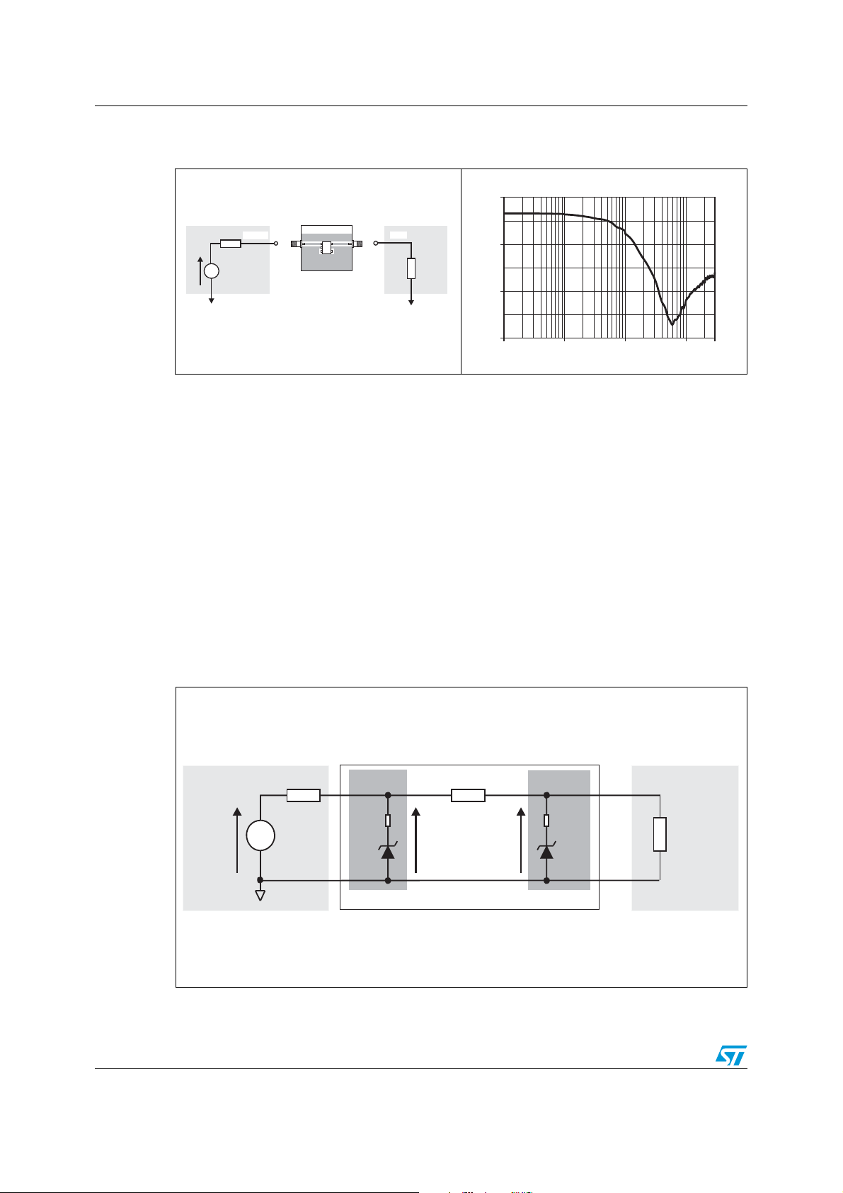
In addition to the requirements of termination and EMC compatibility, computing devices are
required to be tested for ESD susceptibility. This test is described in the IEC 61000-4-2 and
is already in place in Europe. This test requires that a device tolerates ESD events and
remain operational without user intervention.
The USBDFxxW5 is particularly optimized to perform ESD protection. ESD protection is
based on the use of device which clamps at :
V=V+ R.I
INPUT BR d pp
This protection function is split in 2 stages. As shown in Figure 5., the ESD strikes are
clamped by the first stage S1 and then the remaining overvoltage is applied to the second
stage through the resistor R. Such a configuration makes the output voltage very low at the
V
level.
out
TEST BOARD
UD1
RF IN
-10
50 Ω
-20
-30
1 10 100 1000 3000
F (MHz)
Figure 5. USBDFxxW5 ESD clamping behavior
Rg
V
PP
ESD Surge
4/11
S1
Rd
V
BR
R
Vinput
Voutput
USBDFxxW5
S2
Rd
Rload
V
BR
Device
to be
protected
 Loading...