

Page 1
EMI filter and line termination for USB downstream ports
Applications
EMI Filter and line termination for USB
downstream ports on:
■ Desktop computer
■ Notebooks
■ Workstations
■ USB Hubs
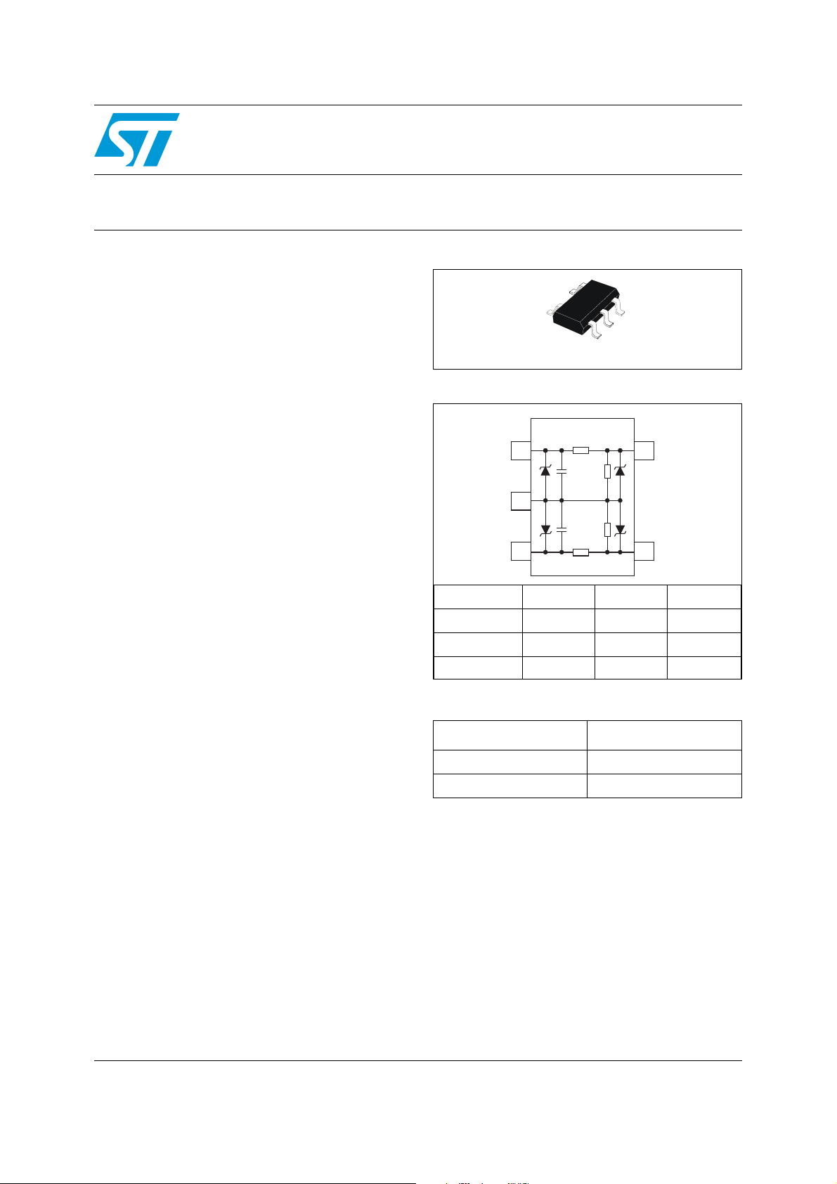
USBDFxxW5
SOT323-5L
Functional diagram
Features
■ Monolithic device with recommended line
termination for USB downstream ports
■ Integrated Rt series termination and Ct
bypassing capacitors.
■ Integrated ESD protection
■ Small package size
Description
The USB specification requires USB downstream
ports to be terminated with pull-down resistors
from the D+ and D- lines to ground. On the
implementation of USB systems, the radiated and
conducted EMI should be kept within the required
levels as stated by the FCC regulations. In
addition to the requirements of termination and
EMC compatibility, the computing devices are
required to be tested for ESD susceptibility.
The USBDFxxW5 provides the recommended line
termination while implementing a low pass filter to
limit EMI levels and providing ESD protection
which exceeds IEC 61000-4-2 level 4 standard.
The device is packaged in a SOT323-5L, which is
a very small (50% smaller than the standard
SOT23).
Complies with the following standards
IEC 61000-4-2, level 4 ±15 kV (air discharge)
±8 kV (contact discharge)
MIL STD 883C, Method 3015-6
Class 3 C = 100 pF R = 1500 W
3 positive strikes and 3 negative strikes (F = 1 Hz)
D+ In
Gnd
D- In
Rt
Ct
Rd
Rd
Ct
Rt
R
t
D+ Out
D- Out
R
d
C
t
USBDF01W5 33 Ω 15 kΩ 47 pF
USBDF02W5 15 Ω 15 kΩ 47 pF
Tolerance ±10% ±10% ±20%
Order codes
Part number Marking
USBDF01W5 UD1
USBDF02W5 UD2
Benefits
■ EMI / RFI noise suppression
■ Required line termination for USB downstream
ports
■ ESD protection exceeding
IEC61000-4-2 level 4
■ IPAD™ technology provides high flexibility in
the design of high density boards
■ Tailored to meet USB 1.1 standard
TM: IPAD is a trademark of STMicroelectronics
September 2006 Rev 3 1/11
www.st.com
11
Page 2
Characteristics USBDFxxW5
1 Characteristics
Table 1. Absolute maximum ratings (T
Symbol Parameter Value Unit
amb
= 25° C)
V
PP
T
T
stg
T
P
Table 2. Electrical characteristics (T
ESD discharge IEC 61000-4-2, contact discharge
ESD discharge - MIL STD 883 - Method 3015-6
Operating junction temperature range -40 to 150 °C
j
Storage temperature range - 55 to +150 °C
Lead solder temperature (10 second duration) 260 °C
L
Power rating per resistor 100 mW
r
Symbol Parameters Test conditions Min Typ Max Unit
V
BR
V
F
Diode breakdown voltage IR = 1 mA 6 V
Diode forward voltage drop IF = 50 mA 0.9 V
2 Application information
Figure 1. USB Standard requirements
Full-speed or
Low-speed USB
Transceiver
Host or
Hub port
Rt
Ct
Rt
15k
Ct
15k
D+
D-
= 25° C)
amb
Twisted pair shielded
Zo = 90ohms
5m max
D+
D-
+Vbus
1.5k
±15
±25
Rt
Full-speed USB
Ct
Rt
Transceiver
Ct
Hub 0 or
Full-speed function
kV
FULL SPEED CONNECTION
Full-speed or
Low-speed USB
Transceiver
Host or
Hub port
Rt
Ct
Rt
15k
Ct
15k
D+
Untwisted unshielded
D-
LOW SPEED CONNECTION
2/11
3m max
D+
D-
+Vbus
1.5k
Rt
Low-speed USB
Ct
Rt
Transceiver
Ct
Hub 0 or
Low-speed function
Page 3

USBDFxxW5 Application information
Figure 2. Application example
Upstream portDownstream port
Host/Hub USB
port transceiver
2.1 EMI filtering
Current FCC regulations requires that class B computing devices meet specified maximum
levels for both radiated and conducted EMI.
● Radiated EMI covers the frequency range from 30 MHz to 1 GHz.
● Conducted EMI covers the 450 kHz to 30 MHz range.
For the types of devices utilizing the USB the most difficult test to pass is usually the
radiated EMI test. For this reason the USBDF device aims to minimize radiated EMI.
The differential signal (D+ and D-) of the USB does not contribute significantly to radiated or
conducted EMI because the magnetic field of the two conductors exactly cancels each
other.
D+
USBDF
xxW5
D-
(1) for a low-speed port
(2) for a full-speed port
CABLE
D+ (1)
D- (2)
+Vbus
D- (1)
D+ (2)
USBUF
xxW6
Peripheral
transceiver
The inside of the PC environment is very noisy and designers must minimise noise coupling
from the different sources. D+ and D- must not be routed near high speed lines (clocks...).
Induced common mode noise can be minimised by running pairs of USB signals parallel to
each other and running grounded guard trace on each side of the signal pair from the USB
controller to the USBDF device.
If possible, locate the USBDF device physically near the USB connectors. Distance between
the USB controller and the USB connector must be minimized.
The 47 pF (C
) capacitors are used to divert high frequency energy to ground and for edge
t
control, and must be placed between the USB Controller and the series termination
resistors (R
). Both Ct and Rt should be placed as close to the mSB Controller as
t
practicable.
The USBDFxxW5 ensure a filtering protection against electroMagnetic and radio-frequency
Interference thanks to its low-pass filter structure. This filter is characterized by the following
parameters :
● cut-off frequency
● Insertion loss
● high frequency rejection
Figure 4. shows the attenuation curve for frequencies up to 3 GHz.
3/11
Page 4
Application information USBDFxxW5
Figure 3. Measurement configuration Figure 4. USBDFxxW5 attenuation
curve
Insertion loss (dB)
0
TG OUT
50 Ω
Vg
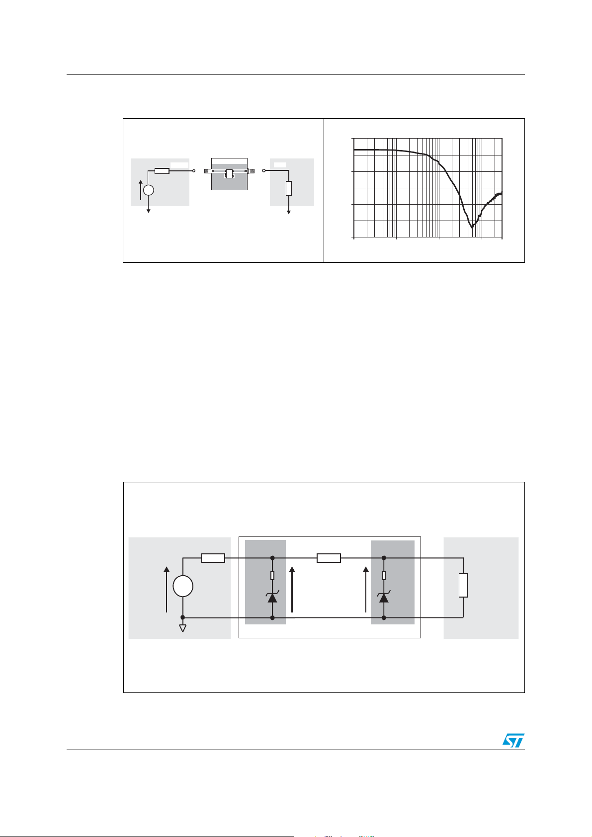
2.2 ESD protection
In addition to the requirements of termination and EMC compatibility, computing devices are
required to be tested for ESD susceptibility. This test is described in the IEC 61000-4-2 and
is already in place in Europe. This test requires that a device tolerates ESD events and
remain operational without user intervention.
The USBDFxxW5 is particularly optimized to perform ESD protection. ESD protection is
based on the use of device which clamps at :
V=V+ R.I
INPUT BR d pp
This protection function is split in 2 stages. As shown in Figure 5., the ESD strikes are
clamped by the first stage S1 and then the remaining overvoltage is applied to the second
stage through the resistor R. Such a configuration makes the output voltage very low at the
V
level.
out
TEST BOARD
UD1
RF IN
-10
50 Ω
-20
-30
1 10 100 1000 3000
F (MHz)
Figure 5. USBDFxxW5 ESD clamping behavior
Rg
V
PP
ESD Surge
4/11
S1
Rd
V
BR
R
Vinput
Voutput
USBDFxxW5
S2
Rd
Rload
V
BR
Device
to be
protected
Page 5

USBDFxxW5 Application information
t
To have a good approximation of the remaining voltages at both Vin and V
the typical dynamical resistance value R
R
> Rd, Rg > R and R
t
R.V + R.V
V=
input
V=
output
gBR d g
R.V + R .V
t BR d inpu
> Rd, gives these formulas::
load
R
g
R
t
The results of the calculation done for V
V
= 7 V (typ.) and Rd = 1 Ω (typ.) give:
BR
V
= 31.2 V
input
V
= 7.95 V
output
. Taking into account the following hypothesis:
d
= 8 kV, Rg = 330 W (IEC61000-4-2 standard),
PP
stages, we give
out
This confirms the very low remaining voltage across the device to be protected. It is also
important to note that in this approximation the parasitic inductance effect was not taken into
account. This could be few tenths of volts during few ns at the V
is not present at the V
side due the low current involved after the resistance R.
out
side. This parasitic effect
in
The measurements results shown below show very clearly (Figure 7.) the high efficiency of
the ESD protection :
● no influence of the parasitic inductances on Vout stage
● output clamping voltage very close to V
(positive strike) and -VF (negative strike)
BR
Figure 6. Measurement board
ESD
SURGE
15 kV
Air
Discharge
TEST BOARD
UD1
Vin Vout
5/11
Page 6

Application information USBDFxxW5
Figure 7. Remaining voltage at both stages S1 (V
surge
A. Positive surge B. Negative surge
Note that the USBDFxxW5 is not only acting for positive ESD surges but also for negative
ones. Negative disturbances are clamped close to ground voltage as shown in Figure 7.b.
2.3 Latch-up phenomena
The early ageing and destruction of IC’s is often due to latch-up phenomena which is mainly
induced by dV/dt. Thanks to its structure, the USBDFxxW5 provides a high immunity to
latch-up phenomena by smoothing very fast edges.
) and S2 (V
input
) during ESD
output
2.4 Crosstalk behaviour
Figure 8. Crosstalk phenomena
R
G1
V
G1
V
G2
The crosstalk phenomena is due to the coupling between 2 lines. The coupling factor ( β12
or β21 ) increases when the gap across lines decreases, this is the reason why we provide
crosstalk measurements for a monolithic device to guarantee negligeable crosstalk between
the lines. In the example above, the expected signal on load R
voltage at this point has got an extra value β21V
the effect of the crosstalk phenomenon of the line 1 on the line 2. This phenomenon has to
be taken into account when the drivers impose fast digital data or high frequency analog
signals in the disturbing line. The perturbed line will be more affected if it works with low
voltage signal or high load impedance (few kΩ).
R
G2
DRIVERS
Line 1
Line 2
R
L1
R
L2
RECEIVERS
. This part of the VG1 signal represents
G1
L2
αβ
V+ V
1 G1 1 2 G2
αβ
V+ V
2 G2 2 1 G1
is α2VG2, in fact the real
6/11
Page 7

USBDFxxW5 Application information
Figure 9. Analog crosstalk measurements Figure 10. Typical analog crosstalk results
Analog crosstalk (dB)
0
TG OUT
50 Ω
Vg
TEST BOARD
UD1
RF IN
50 Ω
-20
-40
-60
-80
-100
1 10 100 1,000
frequency (MHz)
Figure 8. gives the measurement circuit for the analog crosstalk application. In Figure 10.,
the curve shows the effect of the D+ cell on the D- cell. In usual frequency range of analog
signals (up to 100 MHz) the effect on disturbed line is less than -46 dB.
Figure 11. Digital crosstalk measurements
Figure 12. Digital crosstalk results
configuration
+5V +5V
Square
Pulse
Generator
5KHz
+5V
74HC04
Line 1
V
G1
Line 2
USBDF
xxW5
74HC04
b
V
21
G1
Figure 11. shows the measurement circuit used to quantify the crosstalk effect in a classical
digital application.
Figure 12. shows that in such a condition signal, from 0 to 5 V and rise time of few ns, the
impact on the other line is less than 100 mV peak to peak (below the logic high voltage
threshold). The measurements performed with falling edges give the same results.
7/11
Page 8

Application information USBDFxxW5
2.5 Transition times
This low pass filter has been designed in order to meet the USB 1.1 standard requirements
that implies the signal edges are maintained within the 4 ns-20 ns stipulated USB
specification limits.
Figure 13. Typical rise and fall times: measurements configuration
+5V +5V
74HC04
+5V
Square
Pulse
Generator
Figure 14. Typical rise and fall times
74HC04
D+
USBDF
xxW5
D-
A. Rise time B. Fall time
8/11
Page 9

USBDFxxW5 Package information
3 Package information
Table 3. SOT323-5L dimensions
Dimensions
A
E
Ref.
Millimeters Inches
Min. Max. Min. Max.
A 0.8 1.1 0.031 0.043
e
b
e
A1 0 0.1 0 0.004
D
A2 0.8 1 0.031 0.039
b 0.15 0.3 0.006 0.012
A1
A2
Q1
c
L
HE
c 0.1 0.18 0.004 0.007
D 1.8 2.2 0.071 0.086
E 1.15 1.35 0.045 0.053
e 0.65 Typ. 0.025 Typ.
H 1.8 2.4 0.071 0.094
Q1 0.1 0.4 0.004 0.016
Figure 15. Recommended footprint (dimensions in mm)
0.3
1.0
2.9
1.0
0.35
In order to meet environmental requirements, ST offers these devices in ECOPACK®
packages. These packages have a lead-free second level interconnect. The category of
second level interconnect is marked on the package and on the inner box label, in
compliance with JEDEC Standard JESD97. The maximum ratings related to soldering
conditions are also marked on the inner box label. ECOPACK is an ST trademark.
ECOPACK specifications are available at: www.st.com.
9/11
Page 10

Ordering information USBDFxxW5
4 Ordering information
Type Order Code Weight Marking Package Base Qty
USBDF01W5 USBDF01W5
USBDF02W5 USBDF02W5 UD2
5 Revision history
Date Revision Changes
May-2000 1C Initial release.
7-Sep-2006 2
15-Sep-2006 3 Corrected units of R
5.4 mg
SOT323-5L 3000
Reformatted to current standard. Modified Operating junction
temperature range in Table 1.
to kΩ instead of Ω. on page 1
d
UD1
10/11
Page 11

USBDFxxW5
Please Read Carefully:
Information in this document is provided solely in connection with ST products. STMicroelectronics NV and its subsidiaries (“ST”) reserve the
right to make changes, corrections, modifications or improvements, to this document, and the products and services described herein at any
time, without notice.
All ST products are sold pursuant to ST’s terms and conditions of sale.
Purchasers are solely responsible for the choice, selection and use of the ST products and services described herein, and ST assumes no
liability whatsoever relating to the choice, selection or use of the ST products and services described herein.
No license, express or implied, by estoppel or otherwise, to any intellectual property rights is granted under this document. If any part of this
document refers to any third party products or services it shall not be deemed a license grant by ST for the use of such third party products
or services, or any intellectual property contained therein or considered as a warranty covering the use in any manner whatsoever of such
third party products or services or any intellectual property contained therein.
UNLESS OTHERWISE SET FORTH IN ST’S TERMS AND CONDITIONS OF SALE ST DISCLAIMS ANY EXPRESS OR IMPLIED
WARRANTY WITH RESPECT TO THE USE AND/OR SALE OF ST PRODUCTS INCLUDING WITHOUT LIMITATION IMPLIED
WARRANTIES OF MERCHANTABILITY, FITNESS FOR A PARTICULAR PURPOSE (AND THEIR EQUIVALENTS UNDER THE LAWS
OF ANY JURISDICTION), OR INFRINGEMENT OF ANY PATENT, COPYRIGHT OR OTHER INTELLECTUAL PROPERTY RIGHT.
UNLESS EXPRESSLY APPROVED IN WRITING BY AN AUTHORIZED ST REPRESENTATIVE, ST PRODUCTS ARE NOT
RECOMMENDED, AUTHORIZED OR WARRANTED FOR USE IN MILITARY, AIR CRAFT, SPACE, LIFE SAVING, OR LIFE SUSTAINING
APPLICATIONS, NOR IN PRODUCTS OR SYSTEMS WHERE FAILURE OR MALFUNCTION MAY RESULT IN PERSONAL INJURY,
DEATH, OR SEVERE PROPERTY OR ENVIRONMENTAL DAMAGE. ST PRODUCTS WHICH ARE NOT SPECIFIED AS "AUTOMOTIVE
GRADE" MAY ONLY BE USED IN AUTOMOTIVE APPLICATIONS AT USER’S OWN RISK.
Resale of ST products with provisions different from the statements and/or technical features set forth in this document shall immediately void
any warranty granted by ST for the ST product or service described herein and shall not create or extend in any manner whatsoever, any
liability of ST.
ST and the ST logo are trademarks or registered trademarks of ST in various countries.
Information in this document supersedes and replaces all information previously supplied.
The ST logo is a registered trademark of STMicroelectronics. All other names are the property of their respective owners.
© 2006 STMicroelectronics - All rights reserved
STMicroelectronics group of companies
Australia - Belgium - Brazil - Canada - China - Czech Republic - Finland - France - Germany - Hong Kong - India - Israel - Italy - Japan -
Malaysia - Malta - Morocco - Singapore - Spain - Sweden - Switzerland - United Kingdom - United States of America
www.st.com
11/11
 Loading...