


查询USB6B1RL供应商
®
Application Specific Discretes
A.S.D.
APPLICATIONS
Where transient overvoltage protection in sensitive equipment is required, such as:
- Universal Serial Bus ports
- RS-423 interfaces
- RS-485 interfaces
- ISDN equipment
- T1/E1 line cards
- HDSL / ASDL interfaces
FEATURES
Full diode bridge with integrated clamping protection
n
Breakdown voltage : VBR = 6V min.
n
Peakpulsepower dissipation :PPP=500W(8/20µs)
n
Very low capacitance, compatible with high debit
n
data or signal rates.
DESCRIPTION
In order to prevent fast transients from leading
to severe damages in a high speed data system, a specific protection has been developed
by STMicroelectronics.
The USB6Bx protects the two input lines
against overvoltage. Besides, this device also
keeps the power rails in a safe limit thanks to
the integrated Transil diode.
BENEFITS
n
Provides protection for each line and between
the supply voltage and GND : 25A , 8/20µs.
n
High ESD protection level : up to level 3 per
MIL STD 883C-Method 3015-6
n
Separated inputs and outputs (so-called 4-point
structure) to improve ESD susceptibility.
n
Comprehensive package pin-out for immediate
implementation.
COMPLIES WITH THE FOLLOWING STANDARDS:
MIL STD 883C - Method 3015-6
class 3 C = 100 pF R= 1500 Ω
3 positive strikes and 3 negative strikes (F=1Hz)
IEC-1000-4-2 level 4
15 kV (air discharge)
8 kV (contact discharge)
USB6Bx
DATA LINES PROTECTION
SO8
DIL8
FUNCTIONAL DIAGRAM
Vcc
I/01
I/02
GND
Vcc
I/01
I/02
GND
TM: ASDandTRANSIL are trademarks of ST Microelectronics.
August 1999 Ed : 5A
1/9
USB6Bx
TECHNICAL INFORMATION
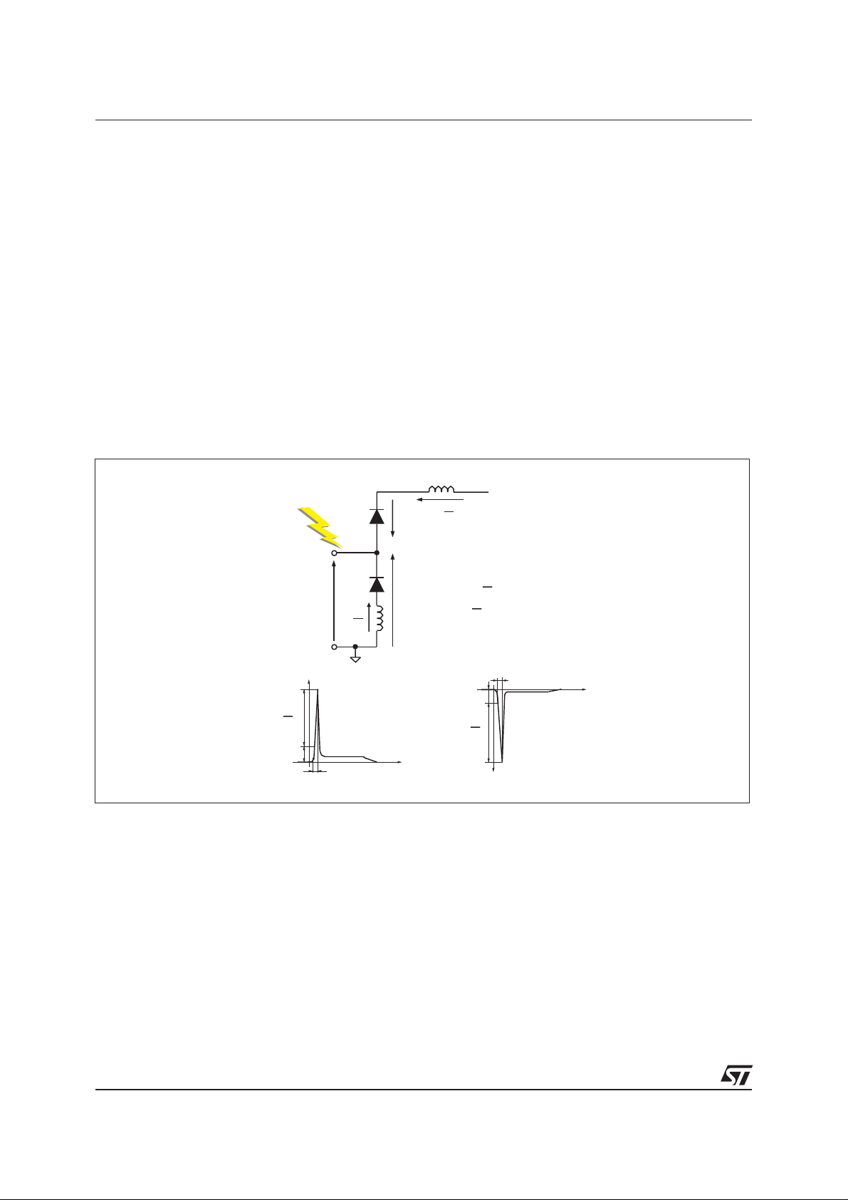
SURGE PROTECTION
The USB6Bx is particularly optimized to perform
surge protection based on the rail to rail topology.
Theclampingvoltage VCLcanbeestimated as follow:
+=Vcc+VFfor positive surges
V
CL
V
CL
-=-V
for negative surges
F
F=Vt
+ rd.Ip
with: V
(V
forward drop voltage) / (Vtforward drop
F
threshold voltage)
Note: the estimations do not take into account
phenomena due to parasitic inductances.
Fig. A1 :
ESD
SURGE
I/O
Lw
Vcc+Vf
VI/O
di
dt
tr=1ns
Vcl+
di
Lw
dt
POSITIVE
SURGE
GND
Vf
Vcl+ =
Vcl- =
t
Lw
di
Lw
dt
Vcc+Vf+
-Vf-
-Lw
Lw
Lw
-Vf
+Vcc
di
surge >0
dt
di
surge <0
dt
tr=1ns
t
NEGATIVE
di
SURGE
dt
Vcl-
2/9
USB6Bx
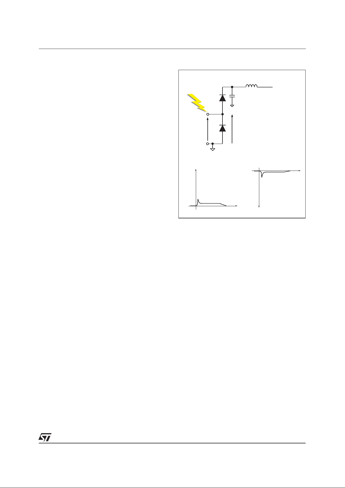
HOW TO ENSURE A GOOD ESD PROTECTION
While the USB6Bx provides a high immunity to
ESD surge, an efficient protection depends on the
layoutofthe board. Inthesame way, withtherail to
rail topology, the track from the V
pin to the
CC
power supply and from the GND pin to GND voltage must be as short as possible to avoid
overvoltages due to parasitic phenomena (see Fig
A1).
It’s often harder to connect the power supply near
to the USB6Bx unlike the ground thanks to the
ground plane that allows a short connection.
To ensure the same efficiency for positive surges
when the connections can’t be short enough, we
recommend to put close to the USB6Bx between
and ground, a capacitance of 100nF to pre-
V
CC
vent from these kinds of overvoltage disturbances
(see Fig. A2 ).
The add of this capacitance will allow a better protection by providing during surge a constant voltage.
Fig. A3 shows the improvement of the ESD protection according to the recommendations described above.
Fig. A2: ESD behavior: optimized layout and add
of a capacitance of 100nF.
C=100nF
Vcl+ =
Vcl- =
t
Lw
Vcc+Vf
-Vf
REF2=+Vcc
surge >0
surge <0
NEGATIVE
SURGE
Vcl-
ESD
SURGE
I/O
VI/O
REF1=GND
Vcl+
POSITIVE
SURGE
IMPORTANT:
A main precaution to take is to put the protection
device closer to the disturbance source (generally
the connection).
t
3/9

USB6Bx
TECHNICAL INFORMATION
Universal Serial Bus.
The new data transmission standard, Universal
SerialBus(USB)is being driven by market leaders
in the world of Computer and Telecommunications, including Compaq, DEC, IBM, Intel,
Microsoft, NEC and Nortel, and will become the
leading transmission protocol within the next few
years.
This standard mainly provides simplified
interconnectivity. Specialized ports on the back of
the present PC will largely be replaced by USB
ports. Many peripherals such as printers, keyboards, monitors and joysticks will also host USB
ports.
The USB offers high speed communication rates
up to 12 Mbit/s. Only two wires (D+, D-) are required for data transfer. Additionally, limited
amount of power for USB devices located on the
Fig. A3: recommended configuration for USB port protection.
downstream can also be transmitted on two separate conductors within the same cable.
Protection to support USB.
Designers dealing with the USB chips are concerned about electrostatic discharge sensitivity
(ESD) of their USB controller ICs.
The USB controller is more than just a driver /
receiver; it acts as a microcontroller which
manages power and direct signal traffic. This
complexity increases its cost over conventional devices. Therefore, a failure of a USB
port could result in costly computer failure.
In order to prevent these fast transients from
leading to severe damages in a system, a
specific protection has been developed by
STMicroelectronics. The USB6Bx protects
not only the two wires of data transmission,
but also keep the power rails in a safe limit.
Vbus
1
D+
D-
GND
USB output
connector
The capacitance between the I/O transmission
wiresprovidesno significant signal distortionatthe
12 Mbit/s data rate, thus allowing full compatibility
with USB standard.
USB
IC
Available either in a compact SO8 or in a
through-hole DIL8 package, this protective element requires minimal board space and eases the
PCB layout thanks to its direct compatibility with
the USB connector pin-out.
4/9

TELECOM AND DATACOM APPLICATIONS
ISDN U interface protection.
USB6Bx
T1 / E1 Line Card Protection.
USB6Bx
+Vcc
LT
DC Power
Source
RTIP
RRING
TTIP
TRING
USB6B1
+Vcc
+Vcc
USB6B1
3* SMP100
SMP75-8 or SMP100-8
SMP75-8 or SMP100-8
High Speed Line Driver / Receiver Protection.
+5V
SM6T6V8A
INPUT
DRIVER
USB6B1
+Vcc
USB6B1
+Vcc
+5V
RECEIVER
SM6T6V8A
OUTPUT
5/9

USB6Bx
ABSOLUTE MAXIMUM RATINGS (T
amb
= 25°C)
Symbol Parameter Value Unit
V
PP
P
PP
I
PP
T
stg
T
j
T
L
ELECTRICAL CHARACTERISTICS (T
Peak pulse voltage
IEC1000-4-2 contact discharge
IEC1000-4-2 air discharge
MIL STD883C-Method 3015-6
Peak pulse power
Peak pulse current
Storage temperature range
Maximum junction temperature
Lead solder temperature (10s duration)
= 25°C)
amb
8
15
4
8/20 µs 500 W
8/20 µs25A
-55to+150
+ 150
260 °C
Value
Symbol Parameter
min. typ. max.
V
BR
Breakdown voltage between V
bus
and
=1mA 6 V
I
R
GND
kV
°C
°C
Unit
I
RM
C
Leakage current
Capacitance between pins D+ and D-
V
=30mV, F=1MHz, VR=0V
OSC
Capacitancebetweenpins D+(orD-) andGND
V
=30mV, F=1MHz, VR=5V
OSC
=5.25V 10 µA
V
RM
V
CC
15 pF
not connected
=5V 25 pF
V
CC
6/9

USB6Bx
Fig 1: Peak power dissipation versus initial junc-
tion temperature.
Ppp[Tj initial]/Ppp[Tj initial=25°C]
1.1
1.0
0.9
0.8
0.7
0.6
0.5
0.4
0.3
0.2
0.1
0.0
-40 -20 0 20 40 60 80 100 120 140 160
Tj initial(°C)
Fig 3: Relativevariationofbreakdownvoltagever-
sus junction temperature (typical values).
VBR[Tj] /VBR[Tj=25°C]
1.10
Fig 2: Relative variation of leakage current versus
junction temperature (typical values).
IR[Tj] / IR[Tj=25°C]
10.0
1.0
Tj(°C)
0.1
-40 -20 0 20 40 60 80 100 120 140
1.05
1.00
0.95
0.90
-40 -20 0 20 40 60 80 100 120 140
Tj(°C)
7/9

USB6Bx
ORDER CODE
USB 6 B1 RL
PACKAGE MECHANICAL DATA.
SO8 Plastic
VBRmin
PACKAGING:
RL = tape and reel.(SO8 only)
= tube
PACKAGE:
1 = SO8
2 = DIL8
DIMENSIONS
REF.
Millimetres Inches
Min. Typ. Max. Min. Typ. Max.
L
A
a2
c1
C
a3
A 1.75 0.069
a1 0.1 0.25 0.004 0.010
a2 1.65 0.065
a3 0.65 0.85 0.025 0.033
b
a
b
e
e3
D
M
S
1
E
1
b 0.35 0.48 0.014 0.019
b1 0.19 0.25 0.007 0.010
C 0.25 0.50 0.50 0.010 0.020
c1 45° (typ)
8
5
F
D 4.8 5.0 0.189 0.197
E 5.8 6.2 0.228 0.244
e 1.27 0.050
1
4
e3 3.81 0.150
F 3.8 4.0 0.15 0.157
L 0.4 1.27 0.016 0.050
M 0.6 0.024
S8⊃(max)
8/9

PACKAGE MECHANICAL DATA.
DIL8 Plastic
I
a1
L
e
B
b
e3
D
8
1
ZZ
5
4
USB6Bx
DIMENSIONS
REF.
a1 0.51 0.020
b1
F
B 0.85 1.40 0.033 0.055
b 0.5 0.020
b1 0.38 0.50 0.015 0.020
E
D 10.15 0.399
E 8.10 8.80 9.40 0.319 0.346 0.370
e 2.54 0.100
e3 7.62 0.300
F 7.1 0.280
I 5.1 0.200
L 3.3 0.130
Z 1.50 0.063
Millimetres Inches
Min. Typ. Max. Min. Typ. Max.
MARKING
Types Package Weight Marking
ORDER
CODE
Base Qty
USB6B1 SO8 0.077g USB62 USB6B1 100 pcs (tube)
USB6B1RL 2500pcs (tape and reel)
USB6B2 DIL8 0.59g USB62 USB6B2 50 pcs (tube)
- Epoxy meets UL94, V0
Informationfurnished is believedto be accurateandreliable. However, STMicroelectronicsassumes no responsibilityforthe consequences of
useof such informationnor for anyinfringement of patentsor other rightsof third partieswhich may resultfromits use. Nolicense is grantedby
implication or otherwise under any patent or patent rights of STMicroelectronics. Specifications mentioned in this publication are subject to
change without notice. This publication supersedes and replaces all information previously supplied.
STMicroelectronics products are not authorized for use as critical components in life support devices or systems without express written approval of STMicroelectronics.
The ST logo is a registered trademark of STMicroelectronics
© 1999 STMicroelectronics - Printed in Italy - All rights reserved.
STMicroelectronics GROUP OF COMPANIES
Australia - Brazil - China - Finland - France - Germany - Hong Kong - India - Italy - Japan - Malaysia
Malta - Morocco - Singapore - Spain - Sweden - Switzerland - United Kingdom - U.S.A.
http://www.st.com
9/9
 Loading...