

ST uPSD3422E-40T6, uPSD3422EV-40T6, uPSD3422E-40U6, uPSD3422EV-40U6, uPSD3433E-40T6 User Manual
...
查询UPSD3422供应商
Fast Turbo 8032 MCU with USB and Programmable Logic
FEATURES SUMMARY
■ FAST 8-BIT TURBO 8032 MCU, 40MHz
– Advanced core, 4-clocks per instruction
– 10 MIPs peak performance at 40MHz (5V)
– JTAG Debug and In-System
Programming
– 16-bit internal instruction path fetches
double-byte instruction in a single memory
cycle
– Branch Cache & 4 instruction Prefetch
Queue
– Dual XDATA pointers with automatic
increment and decrement
– Compatible with 3rd party 8051 tools
■ DUAL FLASH MEMORIES WITH MEMORY
MANAGEMENT
– Place either memory into 8032 program
address space or data address space
– READ-while-WRITE operation for In-
Application Programming and EEPROM
emulation
– Single voltage program and erase
– 100K guaranteed erase cycles, 15-year
retention
■ CLOCK, RESET, AND POWER SUPPLY
MANAGEMENT
– SRAM is Battery Backup capable
– Flexible 8-level CPU clock divider register
– Normal, Idle, and Power Down Modes
– Power-on and Low Voltage reset
supervisor
– Programmable Watchdog Timer
■ PROGRAMMABLE LOGIC, GENERAL
PURPOSE
– 16 macrocells for logic applications (e.g.,
shifters, state machines, chip-selects,
glue-logic to keypads, and LCDs)
■ A/D CONVERTER
– Eight Channels, 10-bit resolution, 6µs
uPSD34xx
Turbo Plus Series
PRELIMINARY DATA
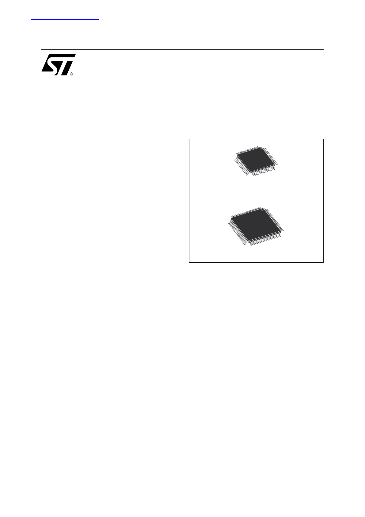
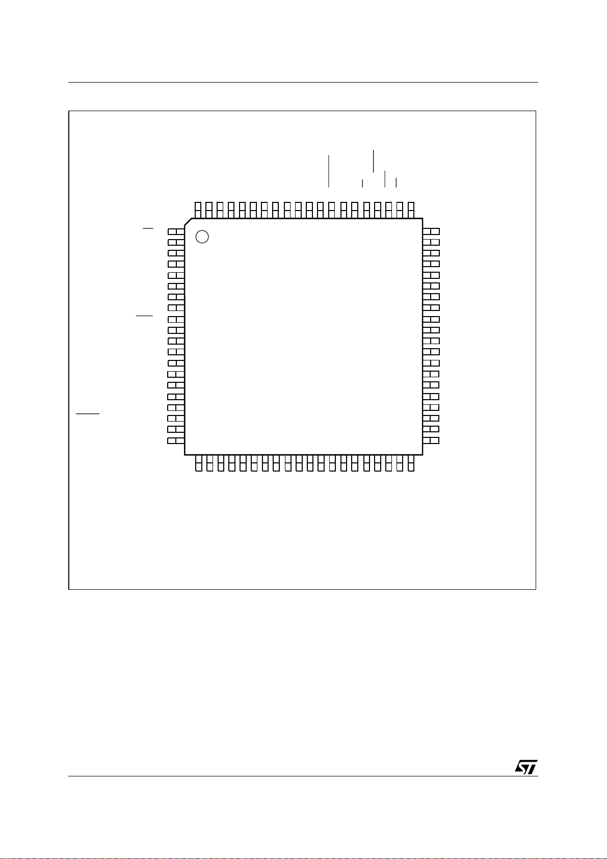
Figure 1. Packages
TQFP52 (T), 52-lead, Thin, Quad, Flat
TQFP80 (U), 80-lead, Thin, Quad, Flat
■ COMMUNICATION INTERFACES
– USB v2.0 Full Speed (12Mbps)
10 endpoint pairs (In/Out), each endpoint
with 64-byte FIFO (supports Control, Intr,
and Bulk transfer types)
2
C Master/Slave controller, 833kHz
–I
– SPI Master controller, 1MHz
– Two UARTs with independent baud rate
– IrDA Potocol: up to 115 kbaud
– Up to 46 I/O, 5V tolerant uPSD34xxV
■ TIMERS AND INTERRUPTS
– Three 8032 standard 16-bit timers
– Programmable Counter Array (PCA), six
16-bit modules for PWM, CAPCOM, and
timers
– 8/10/16-bit PWM operation
– 12 Interrupt sources with two external
interrupt pins
■ OPERATING VOLTAGE SOURCE (±10%)
– 5V Devices: 5.0V and 3.3V sources
– 3.3V Devices: 3.3V source
Rev 2.0
March 2005
This is preliminary information on a new product now in development or undergoing evaluation. Details are subject to change without notice.
1/264
uPSD34xx - FEATURES SUMMARY
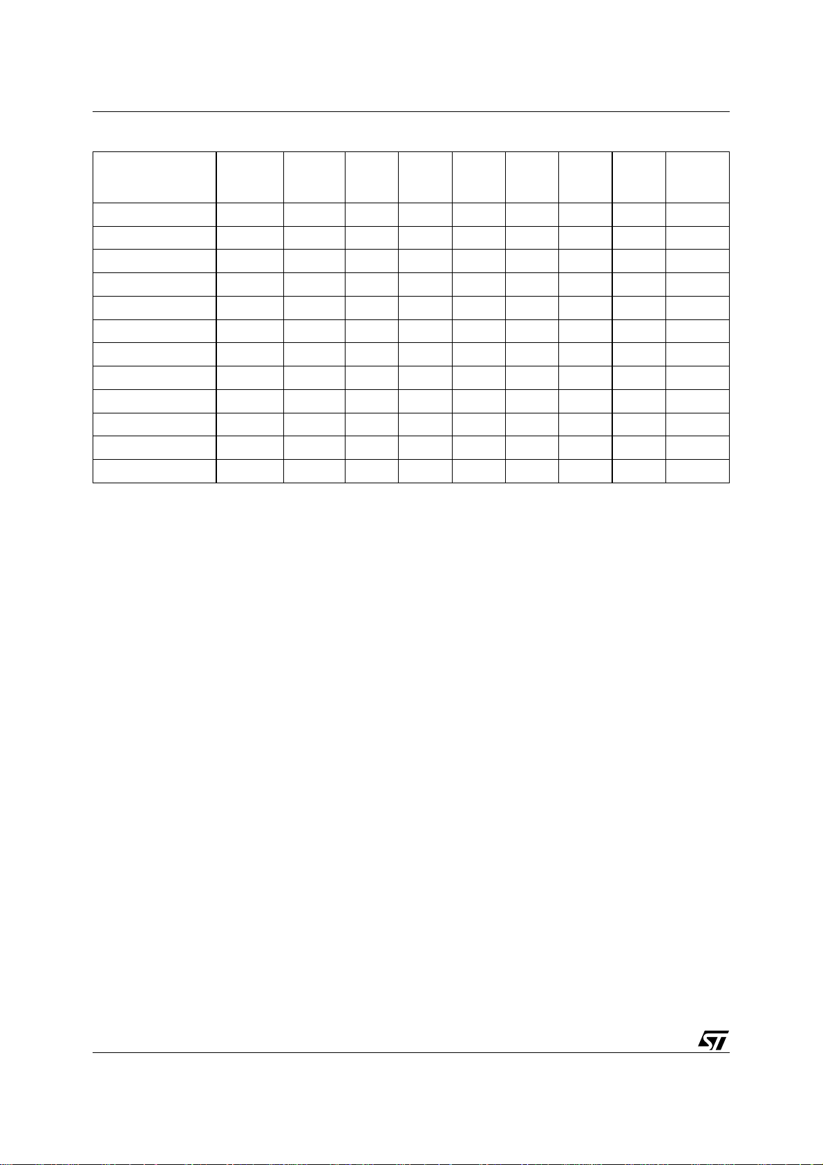
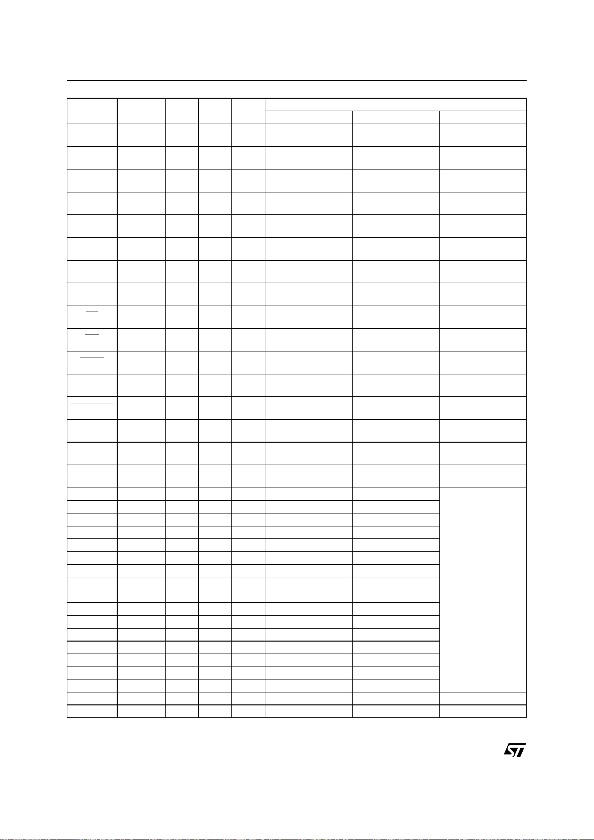
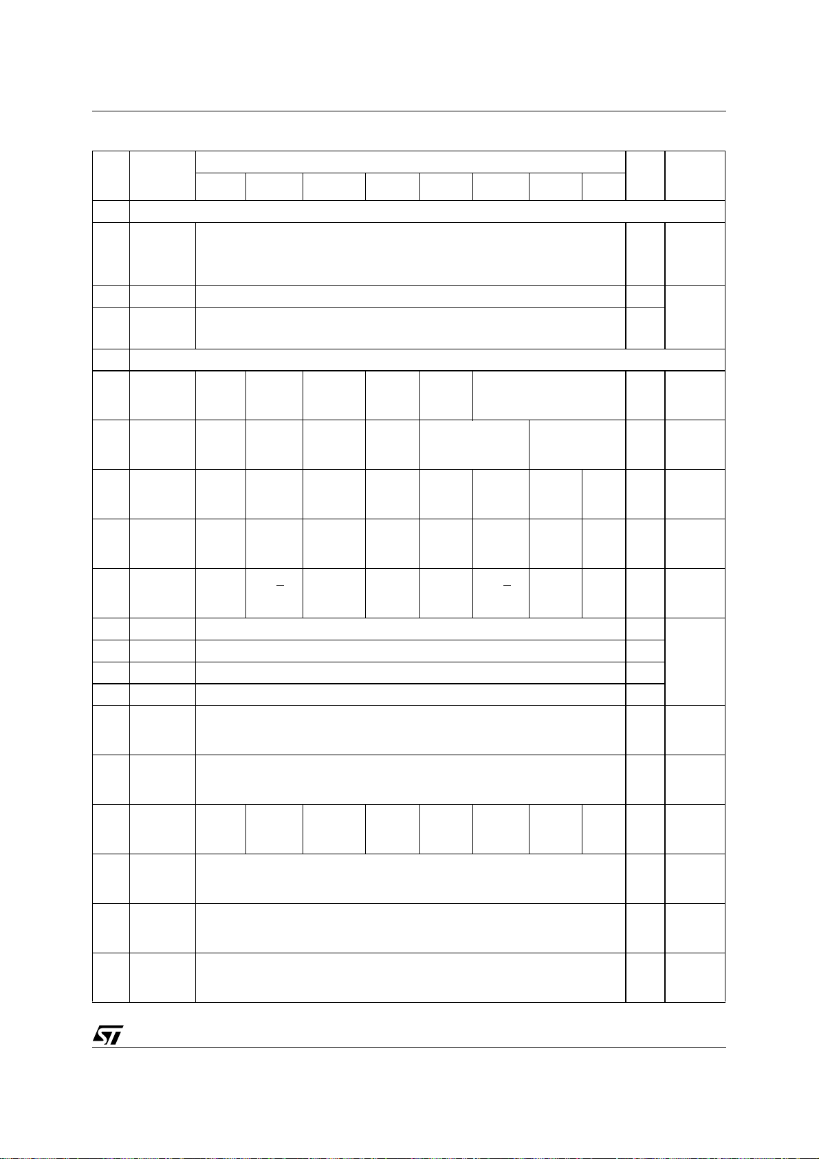
Table 1. Device Summary
1st
Part Number Max MHz
Flash
(bytes)
uPSD3422E-40T6 40 64K 32K 4K 35 No 3.3V 5.0V TQFP52
uPSD3422EV-40T6 40 64K 32K 4K 35 No 3.3V 3.3V TQFP52
uPSD3422E-40U6 40 64K 32K 4K 46 Yes 3.3V 5.0V TQFP80
uPSD3422EV-40U6 40 64K 32K 4K 46 Yes 3.3V 3.3V TQFP80
uPSD3433E-40T6 40 128K 32K 8K 35 No 3.3V 5.0V TQFP52
uPSD3433EV-40T6 40 128K 32K 8K 35 No 3.3V 3.3V TQFP52
uPSD3433E-40U6 40 128K 32K 8K 46 Yes 3.3V 5.0V TQFP80
uPSD3433EV-40U6 40 128K 32K 8K 46 Yes 3.3V 3.3V TQFP80
uPSD3434E-40T6 40 256K 32K 8K 35 No 3.3V 5.0V TQFP52
uPSD3434EV-40T6 40 256K 32K 8K 35 No 3.3V 3.3V TQFP52
uPSD3434E-40U6 40 256K 32K 8K 46 Yes 3.3V 5.0V TQFP80
uPSD3434EV-40U6 40 256K 32K 8K 46 Yes 3.3V 3.3V TQFP80
Note: Operating temperature is in the Industrial range (–40°C to 85°C).
2nd
Flash
SRAM GPIO
8032
Bus
V
CC
V
DD
Pkg.
2/264

uPSD34xx - TABLE OF CONTENTS
TABLE OF CONTENTS
FEATURES SUMMARY . . . . . . . . . . . . . . . . . . . . . . . . . . . . . . . . . . . . . . . . . . . . . . . . . . . . . . . . . . . . . 1
TABLE OF CONTENTS . . . . . . . . . . . . . . . . . . . . . . . . . . . . . . . . . . . . . . . . . . . . . . . . . . . . . . . . . . . . . 3
SUMMARY DESCRIPTION . . . . . . . . . . . . . . . . . . . . . . . . . . . . . . . . . . . . . . . . . . . . . . . . . . . . . . . . . . . 7
PIN DESCRIPTIONS . . . . . . . . . . . . . . . . . . . . . . . . . . . . . . . . . . . . . . . . . . . . . . . . . . . . . . . . . . . . . . . . 9
HARDWARE DESCRIPTION . . . . . . . . . . . . . . . . . . . . . . . . . . . . . . . . . . . . . . . . . . . . . . . . . . . . . . . . 14
MEMORY ORGANIZATION . . . . . . . . . . . . . . . . . . . . . . . . . . . . . . . . . . . . . . . . . . . . . . . . . . . . . . . . . 16
Internal Memory (MCU Module, Standard 8032 Memory: DATA, IDATA, SFR) . . . . . . . . . . . . 17
External Memory (PSD Module: Program memory, Data memory). . . . . . . . . . . . . . . . . . . . . . 17
8032 MCU CORE PERFORMANCE ENHANCEMENTS . . . . . . . . . . . . . . . . . . . . . . . . . . . . . . . . . . . 18
Pre-Fetch Queue (PFQ) and Branch Cache (BC) . . . . . . . . . . . . . . . . . . . . . . . . . . . . . . . . . . . . 20
PFQ Example, Multi-cycle Instructions . . . . . . . . . . . . . . . . . . . . . . . . . . . . . . . . . . . . . . . . . . . . 20
Aggregate Performance . . . . . . . . . . . . . . . . . . . . . . . . . . . . . . . . . . . . . . . . . . . . . . . . . . . . . . . . 20
MCU MODULE DISCRIPTION . . . . . . . . . . . . . . . . . . . . . . . . . . . . . . . . . . . . . . . . . . . . . . . . . . . . . . . 22
8032 MCU REGISTERS . . . . . . . . . . . . . . . . . . . . . . . . . . . . . . . . . . . . . . . . . . . . . . . . . . . . . . . . . . . . 22
Stack Pointer (SP) . . . . . . . . . . . . . . . . . . . . . . . . . . . . . . . . . . . . . . . . . . . . . . . . . . . . . . . . . . . . . 22
Data Pointer (DPTR) . . . . . . . . . . . . . . . . . . . . . . . . . . . . . . . . . . . . . . . . . . . . . . . . . . . . . . . . . . . 22
Program Counter (PC). . . . . . . . . . . . . . . . . . . . . . . . . . . . . . . . . . . . . . . . . . . . . . . . . . . . . . . . . . 22
Accumulator (ACC) . . . . . . . . . . . . . . . . . . . . . . . . . . . . . . . . . . . . . . . . . . . . . . . . . . . . . . . . . . . . 22
B Register (B). . . . . . . . . . . . . . . . . . . . . . . . . . . . . . . . . . . . . . . . . . . . . . . . . . . . . . . . . . . . . . . . . 22
General Purpose Registers (R0 - R7). . . . . . . . . . . . . . . . . . . . . . . . . . . . . . . . . . . . . . . . . . . . . . 23
Program Status Word (PSW) . . . . . . . . . . . . . . . . . . . . . . . . . . . . . . . . . . . . . . . . . . . . . . . . . . . .23
SPECIAL FUNCTION REGISTERS (SFR) . . . . . . . . . . . . . . . . . . . . . . . . . . . . . . . . . . . . . . . . . . . . . . 24
8032 ADDRESSING MODES . . . . . . . . . . . . . . . . . . . . . . . . . . . . . . . . . . . . . . . . . . . . . . . . . . . . . . . . 31
Register Addressing . . . . . . . . . . . . . . . . . . . . . . . . . . . . . . . . . . . . . . . . . . . . . . . . . . . . . . . . . . . 31
Direct Addressing . . . . . . . . . . . . . . . . . . . . . . . . . . . . . . . . . . . . . . . . . . . . . . . . . . . . . . . . . . . . . 31
Register Indirect Addressing . . . . . . . . . . . . . . . . . . . . . . . . . . . . . . . . . . . . . . . . . . . . . . . . . . . . 31
Immediate Addressing . . . . . . . . . . . . . . . . . . . . . . . . . . . . . . . . . . . . . . . . . . . . . . . . . . . . . . . . . 31
External Direct Addressing . . . . . . . . . . . . . . . . . . . . . . . . . . . . . . . . . . . . . . . . . . . . . . . . . . . . . 31
External Indirect Addressing . . . . . . . . . . . . . . . . . . . . . . . . . . . . . . . . . . . . . . . . . . . . . . . . . . . . 31
Indexed Addressing . . . . . . . . . . . . . . . . . . . . . . . . . . . . . . . . . . . . . . . . . . . . . . . . . . . . . . . . . . . 32
Relative Addressing . . . . . . . . . . . . . . . . . . . . . . . . . . . . . . . . . . . . . . . . . . . . . . . . . . . . . . . . . . . 32
Absolute Addressing . . . . . . . . . . . . . . . . . . . . . . . . . . . . . . . . . . . . . . . . . . . . . . . . . . . . . . . . . . 32
Long Addressing . . . . . . . . . . . . . . . . . . . . . . . . . . . . . . . . . . . . . . . . . . . . . . . . . . . . . . . . . . . . . . 32
Bit Addressing . . . . . . . . . . . . . . . . . . . . . . . . . . . . . . . . . . . . . . . . . . . . . . . . . . . . . . . . . . . . . . . . 32
3/264

uPSD34xx - TABLE OF CONTENTS
uPSD34xx INSTRUCTION SET SUMMARY . . . . . . . . . . . . . . . . . . . . . . . . . . . . . . . . . . . . . . . . . . . . 33
DUAL DATA POINTERS. . . . . . . . . . . . . . . . . . . . . . . . . . . . . . . . . . . . . . . . . . . . . . . . . . . . . . . . . . . . 38
Data Pointer Control Register, DPTC (85h) . . . . . . . . . . . . . . . . . . . . . . . . . . . . . . . . . . . . . . . . . 38
Data Pointer Mode Register, DPTM (86h) . . . . . . . . . . . . . . . . . . . . . . . . . . . . . . . . . . . . . . . . . . 39
DEBUG UNIT. . . . . . . . . . . . . . . . . . . . . . . . . . . . . . . . . . . . . . . . . . . . . . . . . . . . . . . . . . . . . . . . . . . . . 40
INTERRUPT SYSTEM. . . . . . . . . . . . . . . . . . . . . . . . . . . . . . . . . . . . . . . . . . . . . . . . . . . . . . . . . . . . . . 41
Individual Interrupt Sources . . . . . . . . . . . . . . . . . . . . . . . . . . . . . . . . . . . . . . . . . . . . . . . . . . . . . 44
MCU CLOCK GENERATION . . . . . . . . . . . . . . . . . . . . . . . . . . . . . . . . . . . . . . . . . . . . . . . . . . . . . . . . 47
MCU_CLK . . . . . . . . . . . . . . . . . . . . . . . . . . . . . . . . . . . . . . . . . . . . . . . . . . . . . . . . . . . . . . . . . . . . 47
PERIPH_CLK . . . . . . . . . . . . . . . . . . . . . . . . . . . . . . . . . . . . . . . . . . . . . . . . . . . . . . . . . . . . . . . . . 47
POWER SAVING MODES . . . . . . . . . . . . . . . . . . . . . . . . . . . . . . . . . . . . . . . . . . . . . . . . . . . . . . . . . . 50
Idle Mode . . . . . . . . . . . . . . . . . . . . . . . . . . . . . . . . . . . . . . . . . . . . . . . . . . . . . . . . . . . . . . . . . . . . 50
Power-down Mode. . . . . . . . . . . . . . . . . . . . . . . . . . . . . . . . . . . . . . . . . . . . . . . . . . . . . . . . . . . . . 50
Reduced Frequency Mode . . . . . . . . . . . . . . . . . . . . . . . . . . . . . . . . . . . . . . . . . . . . . . . . . . . . . . 50
OSCILLATOR AND EXTERNAL COMPONENTS . . . . . . . . . . . . . . . . . . . . . . . . . . . . . . . . . . . . . . . . 53
I/O PORTS of MCU MODULE. . . . . . . . . . . . . . . . . . . . . . . . . . . . . . . . . . . . . . . . . . . . . . . . . . . . . . . . 54
MCU Port Operating Modes . . . . . . . . . . . . . . . . . . . . . . . . . . . . . . . . . . . . . . . . . . . . . . . . . . . . . 54
MCU BUS INTERFACE. . . . . . . . . . . . . . . . . . . . . . . . . . . . . . . . . . . . . . . . . . . . . . . . . . . . . . . . . . . . . 63
PSEN Bus Cycles . . . . . . . . . . . . . . . . . . . . . . . . . . . . . . . . . . . . . . . . . . . . . . . . . . . . . . . . . . . . . 63
READ or WRITE Bus Cycles . . . . . . . . . . . . . . . . . . . . . . . . . . . . . . . . . . . . . . . . . . . . . . . . . . . . .63
Connecting External Devices to the MCU Bus . . . . . . . . . . . . . . . . . . . . . . . . . . . . . . . . . . . . . . 63
Programmable Bus Timing . . . . . . . . . . . . . . . . . . . . . . . . . . . . . . . . . . . . . . . . . . . . . . . . . . . . . . 64
Controlling the PFQ and BC . . . . . . . . . . . . . . . . . . . . . . . . . . . . . . . . . . . . . . . . . . . . . . . . . . . . . 64
SUPERVISORY FUNCTIONS . . . . . . . . . . . . . . . . . . . . . . . . . . . . . . . . . . . . . . . . . . . . . . . . . . . . . . . . 67
External Reset Input Pin, RESET_IN . . . . . . . . . . . . . . . . . . . . . . . . . . . . . . . . . . . . . . . . . . . . . . 67
Low V
Voltage Detect, LVD. . . . . . . . . . . . . . . . . . . . . . . . . . . . . . . . . . . . . . . . . . . . . . . . . . . . 68
CC
Power-up Reset . . . . . . . . . . . . . . . . . . . . . . . . . . . . . . . . . . . . . . . . . . . . . . . . . . . . . . . . . . . . . . . 68
JTAG Debug Reset . . . . . . . . . . . . . . . . . . . . . . . . . . . . . . . . . . . . . . . . . . . . . . . . . . . . . . . . . . . . 68
Watchdog Timer, WDT . . . . . . . . . . . . . . . . . . . . . . . . . . . . . . . . . . . . . . . . . . . . . . . . . . . . . . . . . 68
STANDARD 8032 TIMER/COUNTERS . . . . . . . . . . . . . . . . . . . . . . . . . . . . . . . . . . . . . . . . . . . . . . . . 71
Standard Timer SFRs . . . . . . . . . . . . . . . . . . . . . . . . . . . . . . . . . . . . . . . . . . . . . . . . . . . . . . . . . . 71
Clock Sources . . . . . . . . . . . . . . . . . . . . . . . . . . . . . . . . . . . . . . . . . . . . . . . . . . . . . . . . . . . . . . . . 71
SFR, TCON . . . . . . . . . . . . . . . . . . . . . . . . . . . . . . . . . . . . . . . . . . . . . . . . . . . . . . . . . . . . . . . . . . . 73
SFR, TMOD . . . . . . . . . . . . . . . . . . . . . . . . . . . . . . . . . . . . . . . . . . . . . . . . . . . . . . . . . . . . . . . . . . . 73
Timer 0 and Timer 1 Operating Modes . . . . . . . . . . . . . . . . . . . . . . . . . . . . . . . . . . . . . . . . . . . . 73
Timer 2 . . . . . . . . . . . . . . . . . . . . . . . . . . . . . . . . . . . . . . . . . . . . . . . . . . . . . . . . . . . . . . . . . . . . . . 76
4/264

uPSD34xx - TABLE OF CONTENTS
SERIAL UART INTERFACES . . . . . . . . . . . . . . . . . . . . . . . . . . . . . . . . . . . . . . . . . . . . . . . . . . . . . . . . 83
UART Operation Modes . . . . . . . . . . . . . . . . . . . . . . . . . . . . . . . . . . . . . . . . . . . . . . . . . . . . . . . . 83
Serial Port Control Registers . . . . . . . . . . . . . . . . . . . . . . . . . . . . . . . . . . . . . . . . . . . . . . . . . . . . 84
UART Baud Rates . . . . . . . . . . . . . . . . . . . . . . . . . . . . . . . . . . . . . . . . . . . . . . . . . . . . . . . . . . . . . 86
More About UART Mode 0 . . . . . . . . . . . . . . . . . . . . . . . . . . . . . . . . . . . . . . . . . . . . . . . . . . . . . . 87
More About UART Mode 1 . . . . . . . . . . . . . . . . . . . . . . . . . . . . . . . . . . . . . . . . . . . . . . . . . . . . . . 89
More About UART Modes 2 and 3 . . . . . . . . . . . . . . . . . . . . . . . . . . . . . . . . . . . . . . . . . . . . . . . . 91
IrDA INTERFACE . . . . . . . . . . . . . . . . . . . . . . . . . . . . . . . . . . . . . . . . . . . . . . . . . . . . . . . . . . . . . . . . . 94
Baud Rate Selection . . . . . . . . . . . . . . . . . . . . . . . . . . . . . . . . . . . . . . . . . . . . . . . . . . . . . . . . . . . 95
Pulse Width Selection . . . . . . . . . . . . . . . . . . . . . . . . . . . . . . . . . . . . . . . . . . . . . . . . . . . . . . . . . . 97
2
I
C INTERFACE . . . . . . . . . . . . . . . . . . . . . . . . . . . . . . . . . . . . . . . . . . . . . . . . . . . . . . . . . . . . . . . . . . 98
I2C Interface Main Features . . . . . . . . . . . . . . . . . . . . . . . . . . . . . . . . . . . . . . . . . . . . . . . . . . . . . 98
Communication Flow . . . . . . . . . . . . . . . . . . . . . . . . . . . . . . . . . . . . . . . . . . . . . . . . . . . . . . . . . . 99
Operating Modes . . . . . . . . . . . . . . . . . . . . . . . . . . . . . . . . . . . . . . . . . . . . . . . . . . . . . . . . . . . . . 101
Bus Arbitration . . . . . . . . . . . . . . . . . . . . . . . . . . . . . . . . . . . . . . . . . . . . . . . . . . . . . . . . . . . . . . 101
Clock Synchronization . . . . . . . . . . . . . . . . . . . . . . . . . . . . . . . . . . . . . . . . . . . . . . . . . . . . . . . . 101
General Call Address . . . . . . . . . . . . . . . . . . . . . . . . . . . . . . . . . . . . . . . . . . . . . . . . . . . . . . . . . 101
Serial I/O Engine (SIOE) . . . . . . . . . . . . . . . . . . . . . . . . . . . . . . . . . . . . . . . . . . . . . . . . . . . . . . . 102
2
I
C Interface Control Register (S1CON) . . . . . . . . . . . . . . . . . . . . . . . . . . . . . . . . . . . . . . . . . . 103
2
I
C Interface Status Register (S1STA) . . . . . . . . . . . . . . . . . . . . . . . . . . . . . . . . . . . . . . . . . . . . 105
I2C Data Shift Register (S1DAT). . . . . . . . . . . . . . . . . . . . . . . . . . . . . . . . . . . . . . . . . . . . . . . . . 107
2
I
C Address Register (S1ADR) . . . . . . . . . . . . . . . . . . . . . . . . . . . . . . . . . . . . . . . . . . . . . . . . . . 107
2
I
C START Sample Setting (S1SETUP) . . . . . . . . . . . . . . . . . . . . . . . . . . . . . . . . . . . . . . . . . . . 108
2
I
C Operating Sequences . . . . . . . . . . . . . . . . . . . . . . . . . . . . . . . . . . . . . . . . . . . . . . . . . . . . . . 111
SPI (SYNCHRONOUS PERIPHERAL INTERFACE) . . . . . . . . . . . . . . . . . . . . . . . . . . . . . . . . . . . . . 115
SPI Bus Features and Communication Flow . . . . . . . . . . . . . . . . . . . . . . . . . . . . . . . . . . . . . . 116
Full-Duplex Operation . . . . . . . . . . . . . . . . . . . . . . . . . . . . . . . . . . . . . . . . . . . . . . . . . . . . . . . . . 116
Bus-Level Activity . . . . . . . . . . . . . . . . . . . . . . . . . . . . . . . . . . . . . . . . . . . . . . . . . . . . . . . . . . . . 116
SPI SFR Registers . . . . . . . . . . . . . . . . . . . . . . . . . . . . . . . . . . . . . . . . . . . . . . . . . . . . . . . . . . . . 118
SPI Configuration . . . . . . . . . . . . . . . . . . . . . . . . . . . . . . . . . . . . . . . . . . . . . . . . . . . . . . . . . . . . 119
Dynamic Control . . . . . . . . . . . . . . . . . . . . . . . . . . . . . . . . . . . . . . . . . . . . . . . . . . . . . . . . . . . . . 119
USB INTERFACE . . . . . . . . . . . . . . . . . . . . . . . . . . . . . . . . . . . . . . . . . . . . . . . . . . . . . . . . . . . . . . . . 123
Basic USB Concepts . . . . . . . . . . . . . . . . . . . . . . . . . . . . . . . . . . . . . . . . . . . . . . . . . . . . . . . . . . 124
Types of Transfers . . . . . . . . . . . . . . . . . . . . . . . . . . . . . . . . . . . . . . . . . . . . . . . . . . . . . . . . . . . 127
Endpoint FIFOs . . . . . . . . . . . . . . . . . . . . . . . . . . . . . . . . . . . . . . . . . . . . . . . . . . . . . . . . . . . . . . 129
USB Registers . . . . . . . . . . . . . . . . . . . . . . . . . . . . . . . . . . . . . . . . . . . . . . . . . . . . . . . . . . . . . . . 132
Typical Connection to USB . . . . . . . . . . . . . . . . . . . . . . . . . . . . . . . . . . . . . . . . . . . . . . . . . . . . 150
ANALOG-TO-DIGITAL CONVERTOR (ADC) . . . . . . . . . . . . . . . . . . . . . . . . . . . . . . . . . . . . . . . . . . 151
Port 1 ADC Channel Selects . . . . . . . . . . . . . . . . . . . . . . . . . . . . . . . . . . . . . . . . . . . . . . . . . . . . 151
5/264

uPSD34xx - TABLE OF CONTENTS
PROGRAMMABLE COUNTER ARRAY (PCA) WITH PWM . . . . . . . . . . . . . . . . . . . . . . . . . . . . . . . 154
PCA Block . . . . . . . . . . . . . . . . . . . . . . . . . . . . . . . . . . . . . . . . . . . . . . . . . . . . . . . . . . . . . . . . . . 154
PCA Clock Selection . . . . . . . . . . . . . . . . . . . . . . . . . . . . . . . . . . . . . . . . . . . . . . . . . . . . . . . . . . 156
Operation of TCM Modes . . . . . . . . . . . . . . . . . . . . . . . . . . . . . . . . . . . . . . . . . . . . . . . . . . . . . . 157
Capture Mode. . . . . . . . . . . . . . . . . . . . . . . . . . . . . . . . . . . . . . . . . . . . . . . . . . . . . . . . . . . . . . . . 157
Timer Mode . . . . . . . . . . . . . . . . . . . . . . . . . . . . . . . . . . . . . . . . . . . . . . . . . . . . . . . . . . . . . . . . . 157
Toggle Mode . . . . . . . . . . . . . . . . . . . . . . . . . . . . . . . . . . . . . . . . . . . . . . . . . . . . . . . . . . . . . . . . 157
PWM Mode - (X8), Fixed Frequency . . . . . . . . . . . . . . . . . . . . . . . . . . . . . . . . . . . . . . . . . . . . . . 157
PWM Mode - (X8), Programmable Frequency . . . . . . . . . . . . . . . . . . . . . . . . . . . . . . . . . . . . . . 159
PWM Mode - Fixed Frequency, 16-bit . . . . . . . . . . . . . . . . . . . . . . . . . . . . . . . . . . . . . . . . . . . . 160
PWM Mode - Fixed Frequency, 10-bit . . . . . . . . . . . . . . . . . . . . . . . . . . . . . . . . . . . . . . . . . . . . 160
Writing to Capture/Compare Registers . . . . . . . . . . . . . . . . . . . . . . . . . . . . . . . . . . . . . . . . . . . 160
Control Register Bit Definition . . . . . . . . . . . . . . . . . . . . . . . . . . . . . . . . . . . . . . . . . . . . . . . . . . 160
TCM Interrupts . . . . . . . . . . . . . . . . . . . . . . . . . . . . . . . . . . . . . . . . . . . . . . . . . . . . . . . . . . . . . . . 163
PSD MODULE . . . . . . . . . . . . . . . . . . . . . . . . . . . . . . . . . . . . . . . . . . . . . . . . . . . . . . . . . . . . . . . . . . . 164
PSD Module Functional Description . . . . . . . . . . . . . . . . . . . . . . . . . . . . . . . . . . . . . . . . . . . . . 165
Memory Mapping . . . . . . . . . . . . . . . . . . . . . . . . . . . . . . . . . . . . . . . . . . . . . . . . . . . . . . . . . . . . . 169
PSD Module Data Bus Width . . . . . . . . . . . . . . . . . . . . . . . . . . . . . . . . . . . . . . . . . . . . . . . . . . . 175
Runtime Control Register Definitions (csiop). . . . . . . . . . . . . . . . . . . . . . . . . . . . . . . . . . . . . . 176
PSD Module Detailed Operation. . . . . . . . . . . . . . . . . . . . . . . . . . . . . . . . . . . . . . . . . . . . . . . . . 178
PSD Module Reset Conditions . . . . . . . . . . . . . . . . . . . . . . . . . . . . . . . . . . . . . . . . . . . . . . . . . . 224
AC/DC PARAMETERS . . . . . . . . . . . . . . . . . . . . . . . . . . . . . . . . . . . . . . . . . . . . . . . . . . . . . . . . . . . . 233
MAXIMUM RATING. . . . . . . . . . . . . . . . . . . . . . . . . . . . . . . . . . . . . . . . . . . . . . . . . . . . . . . . . . . . . . . 235
DC AND AC PARAMETERS. . . . . . . . . . . . . . . . . . . . . . . . . . . . . . . . . . . . . . . . . . . . . . . . . . . . . . . . 235
PACKAGE MECHANICAL INFORMATION . . . . . . . . . . . . . . . . . . . . . . . . . . . . . . . . . . . . . . . . . . . . 257
PART NUMBERING . . . . . . . . . . . . . . . . . . . . . . . . . . . . . . . . . . . . . . . . . . . . . . . . . . . . . . . . . . . . . . 261
IMPORTANT NOTES . . . . . . . . . . . . . . . . . . . . . . . . . . . . . . . . . . . . . . . . . . . . . . . . . . . . . . . . . . . . . 262
USB Interrupts with Idle Mode . . . . . . . . . . . . . . . . . . . . . . . . . . . . . . . . . . . . . . . . . . . . . . . . . . 262
USB Reset Interrupt . . . . . . . . . . . . . . . . . . . . . . . . . . . . . . . . . . . . . . . . . . . . . . . . . . . . . . . . . . 262
USB Reset . . . . . . . . . . . . . . . . . . . . . . . . . . . . . . . . . . . . . . . . . . . . . . . . . . . . . . . . . . . . . . . . . . 262
. . . . . . . . . . . . . . . . . . . . . . . . . . . . . . . . . . . . . . . . . . . . . . . . . . . . . . . . . . . . . . . . . . . . . . . . . . . . 262
Data Toggle . . . . . . . . . . . . . . . . . . . . . . . . . . . . . . . . . . . . . . . . . . . . . . . . . . . . . . . . . . . . . . . . . 262
USB FIFO Accessibility . . . . . . . . . . . . . . . . . . . . . . . . . . . . . . . . . . . . . . . . . . . . . . . . . . . . . . . . 262
Erroneous Resend of Data Packet . . . . . . . . . . . . . . . . . . . . . . . . . . . . . . . . . . . . . . . . . . . . . . . 262
IN FIFO Pairing Operation. . . . . . . . . . . . . . . . . . . . . . . . . . . . . . . . . . . . . . . . . . . . . . . . . . . . . . 263
PORT 1 Not 5-volt IO Tolerant . . . . . . . . . . . . . . . . . . . . . . . . . . . . . . . . . . . . . . . . . . . . . . . . . . 263
REVISION HISTORY . . . . . . . . . . . . . . . . . . . . . . . . . . . . . . . . . . . . . . . . . . . . . . . . . . . . . . . . . . . . . . 264
6/264

SUMMARY DESCRIPTION
The Turbo Plus uPSD34xx Series combines a
powerful 8051-based microcontroller with a flexible memory structure, programmable logic, and a
rich peripheral mix to form an ideal embedded
controller. At its core is a fast 4-cycle 8032 MCU
with a 4-byte instruction prefetch queue (PFQ) and
a 4-entry fully associative branching cache (BC).
The MCU is connected to a 16-bit internal instruction path to maximize performance, enabling loops
of code in smaller localities to execute extremely
fast. The 16-bit wide instruction path in the Turbo
Plus Series allows double-byte instructions to be
fetched from memory in a single memory cycle.
This keeps the average performance near its peak
performance (peak performance for 5V, 40MHz
Turbo Plus uPSD34xx is 10 MIPS for single-byte
instructions, and average performance will be approximately 9 MIPS for mix of single- and multibyte instructions).
USB 2.0 (full speed, 12Mbps) is included, providing 10 endpoints, each with its own 64-byte FIFO
to maintain high data throughput. Endpoint 0 (Control Endpoint) uses two of the 10 endpoints for In
and Out directions, the remaining eight endpoints
may be allocated in any mix to either type of transfers: Bulk or Interrupt.
Code development is easily managed without a
hardware In-Circuit Emulator by using the serial
uPSD34xx - SUMMARY DESCRIPTION
JTAG debug interface. JTAG is also used for InSystem Programming (ISP) in as little as 10 seconds, perfect for manufacturing and lab development. The 8032 core is coupled to Programmable
System Device (PSD) architecture to optimize the
8032 memory structure, offering two independent
banks of Flash memory that can be placed at virtually any address within 8032 program or data address space, and easily paged beyond 64K bytes
using on-chip programmable decode logic.
Dual Flash memory banks provide a robust solution for remote product updates in the field through
In-Application Programming (IAP). Dual Flash
banks also support EEPROM emulation, eliminating the need for external EEPROM chips.
General purpose programmable logic (PLD) is included to build an endless variety of glue-logic,
saving external logic devices. The PLD is configured using the software development tool, PSDsoft Express, available from the web at
www.st.com/psm, at no charge.
The uPSD34xx also includes supervisor functions
such as a programmable watchdog timer and lowvoltage reset.
Note: For a list of known limitations of the
uPSD34xx devices, please refer to IMPORTANT
NOTES, page 262.
7/264
uPSD34xx - SUMMARY DESCRIPTION
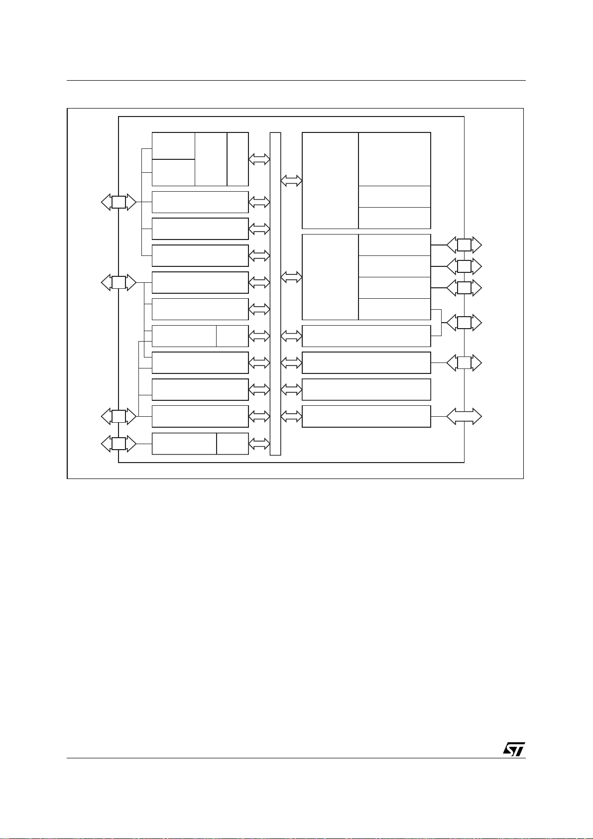
Figure 2. Block Diagram
(3) 16-bit
Timer/
Counters
(2)
External
Interrupts
P3.0:7
P1.0:7
Optional IrDA
Encoder/Decoder
Turbo
8032
Core
I2C
UART0
(8) GPIO, Port 3
(8) GPIO, Port 1
(8) 10-bit ADC
PFQ
&
BC
UART1
uPSD34xx
Programmable
Programmable
SYSTEM BUS
Decode and
Page Logic
General
Purpose
Logic,
16 Macrocells
JTAG ICE and ISP
1st Flash Memory:
64K, 128K, or
256K Bytes
2nd Flash Memory:
32K Bytes
SRAM:
4K or 8K Bytes
(8) GPIO, Port A
(80-pin only)
(8) GPIO, Port B
(2) GPIO, Port D
(4) GPIO, Port C
PA0:7
PB0:7
PD1:2
PC0:7
P4.0:7
USB+,
USB–
SPI
16-bit PCA
(6) PWM, CAPCOM, TIMER
(8) GPIO, Port 4
USB v2.0,
Full Speed
10
FIFOs
8032 Address/Data/Control Bus
(80-pin device only)
Supervisor:
Watchdog and Low-Voltage Reset
VCC, VDD, GND, Reset, Crystal In
MCU
Bus
Dedicated
Pins
AI09695
8/264
PIN DESCRIPTIONS
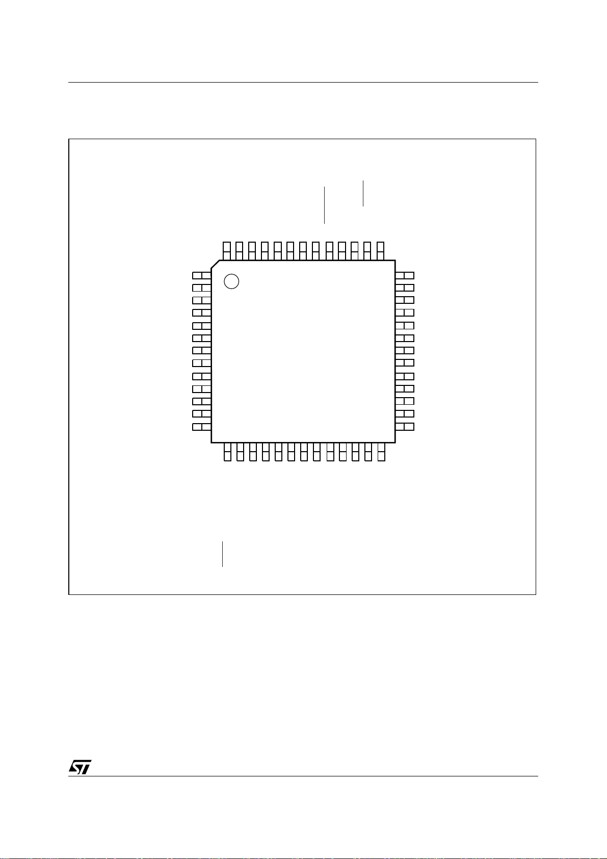
Figure 3. TQFP52 Connections
uPSD34xx - PIN DESCRIPTIONS
/ADC7
(2)
PB6
(2)
PB7
P1.7/SPISEL
(3)
REF
/V
CC
PB5
GND
PB0
PB1
PB2
PB3
PB4
AV
RESET_IN
52515049484746454443424140
/ADC6
P1.6/SPITXD
PD1/CLKIN
PC7
JTAG TDO
JTAG TDI
DEBUG
3.3V V
CC
USB+
V
DD
GND
USB–
PC2/V
STBY
JTAG TCK
JTAG TMS
(2)
(2)
(2)
(2)
/ADC1
/ADC0
/ADC5
/ADC4
(2)
/ADC3
(2)
/ADC2
1
2
3
4
5
6
7
(1)
8
9
10
11
12
13
39 P1.5/SPIRXD
38 P1.4/SPICLK
37 P1.3/TXD1(IrDA)
36 P1.2/RXD1(IrDA)
35 P1.1/T2X
34 P1.0/T2
(1)
33 V
DD
32 XTAL2
31 XTAL1
30 P3.7/SCL
29 P3.6/SDA
28 P3.5/C1
27 P3.4/C0
14151617181920212223242526
GND
TXD0/P3.1
/TCM4/P4.5
/TCM5/P4.6
/TCM3/P4.4
(2)
(2)
SPITXD
SPIRXD
(2)
SPICLK
/PCACLK1/P4.7
(2)
SPISEL
/TCM2/P4.2
(2)
/PCACLK0/P4.3
(2)
RXD1(IrDA)
TXD1(IrDA)
RXD0/P3.0
/TCM1/P4.1
/TCM0/P4.0
(2)
(2)
T2
T2X
EXTINT0/TG0/P3.2
EXTINT1/TG1/P3.3
AI09696
Note: 1. For 5V applications, VDD must be connected to a 5.0V source. For 3.3V applications, VDD must be connected to a 3.3V source.
2. These signals can be used on one of two different ports (Port 1 or Port 4) for flexibility. Default is Port1.
3. AV
and 3.3V AVCC are shared in the 52-pin package only. ADC channels must use 3.3V as AV
REF
for the 52-pin package.
REF
9/264
uPSD34xx - PIN DESCRIPTIONS
Figure 4. TQFP80 Connections
SPISEL
SPITXD
PD2/CSI
P3.3/TG1/EXINT1
PD1/CLKIN
ALE
PC7
JTAG TDO
JTAG TDI
DEBUG
PC4/TERR
3.3V V
USB+
V
DD
GND
USB–
PC3/TSTAT
PC2/V
STBY
JTAG TCK
(2)
/PCACLK1/P4.7
(2)
/TCM5/P4.6
JTAG TMS
/ADC7
(3)
CC
PB0
P3.2/EXINT0/TG0
PB1
P3.1/TXD0
PB2
P3.0/RXD0
PB3
PB4
AV
PB5
V
REF
GND
RESET_IN
PB6
PB7RDP1.7/SPISEL
80797877767574737271706968676665646362
1
2
3
4
5
6
7
8
9
10
CC
(1)
11
(2)
12
13
14
15
16
17
18
19
20
/ADC6
(3)
PSENWRP1.6/SPITXD
61
60 P1.5/SPIRXD
59 P1.4/SPICLK
58 P1.3/TXD1(IrDA)
57 NC
56 P1.2/RXD1(IrDA)
55 NC
54 P1.1/T2X
53 NC
52 P1.0/T2
51 NC
50 V
49 XTAL2
48 XTAL1
47 MCU AD7
46 P3.7/SCL
45 MCU AD6
44 P3.6/SDA
43 MCU AD5
42 P3.5/C1
41 MCU AD4
(3)
/ADC5
(3)
/ADC4
(3)
/ADC3
(3)
/ADC2
(3)
/ADC1
(3)
/ADC0
(1)
DD
21222324252627282930313233343536373839
PA7
PA6
/TCM4/P4.5
(2)
SPIRXD
PA5
/TCM3/P4.4
(2)
SPICLK
PA3
PA4
/PCACLK0/P4.3
(2)
GND
PA2
/TCM1/P4.1
/TCM2/P4.2
(2)
(2)
T2X
PA1
PA0
/TCM0/P4.0
(2)
T2
MCU AD0
MCU AD1
MCU AD2
RXD1(IrDA)
TXD1(IrDA)
Note: NC = Not Connected
Note: 1. The USB+ pin needs a 1.5kΩ pull-up resistor.
2. For 5V applications, V
3. These signals can be used on one of two different ports (Port 1 or Port 4) for flexibility. Default is Port1.
must be connected to a 5.0V source. For 3.3V applications, VDD must be connected to a 3.3V source.
DD
10/264
40
P3.4/C0
MCU AD3
AI09697

uPSD34xx - PIN DESCRIPTIONS
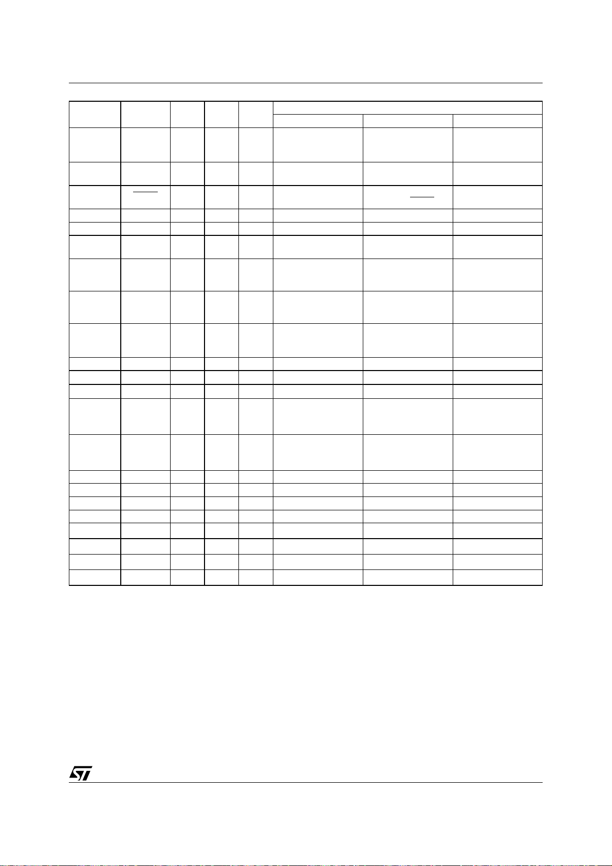
Table 2. Pin Definitions
Function
Timer 2 Count input
(T2)
Timer 2 Trigger input
(T2X)
UART1 or IrDA
Receive (RxD1)
UART or IrDA
Transmit (TxD1)
SPI Clock Out
(SPICLK)
SPI Receive
(SPIRxD)
SPI Transmit
(SPITxD)
SPI Slave Select
(SPISEL)
UART0 Receive
(RxD0)
UART0 Transmit
(TxD0)
Interrupt 0 input
(EXTINT0)/Timer 0
gate control (TG0)
Interrupt 1 input
(EXTINT1)/Timer 1
gate control (TG1)
2
C Bus serial data
I
2
CSDA)
(I
2
I
C Bus clock
2
CSCL)
(I
Program Counter
Array0 PCA0-TCM0
Port Pin
Signal
Name
80-Pin
No.
52-Pin
(1)
No.
In/Out
Basic Alternate 1 Alternate 2
External Bus
MCUAD0 AD0 36 N/A I/O
Multiplexed Address/
Data bus A0/D0
MCUAD1 AD1 37 N/A I/O
MCUAD2 AD2 38 N/A I/O
MCUAD3 AD3 39 N/A I/O
MCUAD4 AD4 41 N/A I/O
MCUAD5 AD5 43 N/A I/O
MCUAD6 AD6 45 N/A I/O
MCUAD7 AD7 47 N/A I/O
P1.0
P1.1
P1.2
P1.3
P1.4
P1.5
P1.6
P1.7
T2
ADC0
T2X
ADC1
RxD1
ADC2
TXD1
ADC3
SPICLK
ADC4
SPIRxD
ADC6
SPITXD
ADC6
SPISEL
ADC7
52 34 I/O General I/O port pin
54 35 I/O General I/O port pin
56 36 I/O General I/O port pin
58 37 I/O General I/O port pin
59 38 I/O General I/O port pin
60 39 I/O General I/O port pin
61 40 I/O General I/O port pin
64 41 I/O General I/O port pin
Multiplexed Address/
Data bus A1/D1
Multiplexed Address/
Data bus A2/D2
Multiplexed Address/
Data bus A3/D3
Multiplexed Address/
Data bus A4/D4
Multiplexed Address/
Data bus A5/D5
Multiplexed Address/
Data bus A6/D6
Multiplexed Address/
Data bus A7/D7
P3.0 RxD0 75 23 I/O General I/O port pin
P3.1 TXD0 77 24 I/O General I/O port pin
P3.2
EXINT0
TGO
79 25 I/O General I/O port pin
P3.3 INT1 2 26 I/O General I/O port pin
P3.4 C0 40 27 I/O General I/O port pin Counter 0 input (C0)
P3.5 C1 42 28 I/O General I/O port pin Counter 1 input (C1)
P3.6 SDA 44 29 I/O General I/O port pin
P3.7 SCL 46 30 I/O General I/O port pin
P4.0
T2
TCM0
33 22 I/O General I/O port pin
ADC Channel 0
input (ADC0)
ADC Channel 1
input (ADC1)
ADC Channel 2
input (ADC2)
ADC Channel 3
input (ADC3)
ADC Channel 4
input (ADC4)
ADC Channel 5
input (ADC5)
ADC Channel 6
input (ADC6)
ADC Channel 7
input (ADC7)
Timer 2 Count input
(T2)
11/264
uPSD34xx - PIN DESCRIPTIONS
Port Pin
P4.1
P4.2
P4.3
P4.4
P4.5
Signal
Name
T2X
TCM1
RXD1
TCM2
TXD1
PCACLK0
SPICLK
TCM3
SPIRXD
TCM4
80-Pin
No.
52-Pin
No.
(1)
In/Out
Basic Alternate 1 Alternate 2
31 21 I/O General I/O port pin PCA0-TCM1
30 20 I/O General I/O port pin PCA0-TCM2
27 18 I/O General I/O port pin PCACLK0
25 17 I/O General I/O port pin
Program Counter
Array1 PCA1-TCM3
23 16 I/O General I/O port pin PCA1-TCM4
P4.6 SPITXD 19 15 I/O General I/O port pin PCA1-TCM5
P4.7
V
REF
RD
WR
PSEN
ALE 4 N/A O
RESET_IN
XTAL1 48 31 I
XTAL2 49 32 O
DEBUG 8 5 I/O
SPISEL
PCACLK1
18 14 I/O General I/O port pin PCACLK1
70 N/A I
65 N/A O
62 N/A O
63 N/A O
Reference Voltage
input for ADC
READ Signal,
external bus
WRITE Signal,
external bus
PSEN Signal,
external bus
Address Latch
signal, external bus
68 44 I
Active low reset
input
Oscillator input pin
for system clock
Oscillator output pin
for system clock
I/O to the MCU
Debug Unit
PA0 35 N/A I/O General I/O port pin
PA1 34 N/A I/O General I/O port pin
PA2 32 N/A I/O General I/O port pin
PA3 28 N/A I/O General I/O port pin
PA4 26 N/A I/O General I/O port pin
PA5 24 N/A I/O General I/O port pin
PA6 22 N/A I/O General I/O port pin
PA7 21 N/A I/O General I/O port pin
PB0 80 52 I/O General I/O port pin
PB1 78 51 I/O General I/O port pin
PB2 76 50 I/O General I/O port pin
PB3 74 49 I/O General I/O port pin
PB4 73 48 I/O General I/O port pin
PB5 71 46 I/O General I/O port pin
PB6 67 43 I/O General I/O port pin
PB7 66 42 I/O General I/O port pin
JTAGTMS TMS 20 13 I JTAG pin (TMS)
JTAGTCK TCK 17 12 I JTAG pin (TCK)
Function
Timer 2 Trigger input
(T2X)
UART1 or IrDA
Receive (RxD1)
UART1 or IrDA
Transmit (TxD1)
SPI Clock Out
(SPICLK)
SPI Receive
(SPIRxD)
SPI Transmit
(SPITxD)
SPI Slave Select
(SPISEL)
All Port A pins
support:
1. PLD Macro-cell
outputs, or
2. PLD inputs, or
3. Latched
Address Out
(A0-A7), or
4. Peripheral I/O
Mode
All Port B pins
support:
1. PLD Macro-cell
outputs, or
2. PLD inputs, or
3. Latched
Address Out
(A0-A7)
12/264
uPSD34xx - PIN DESCRIPTIONS
Port Pin
PC2
Signal
Name
V
STBY
80-Pin
No.
52-Pin
No.
(1)
In/Out
Basic Alternate 1 Alternate 2
16 11 I/O General I/O port pin
PC3 TSTAT 15 N/A I/O General I/O port pin
PC4 TERR
9 N/A I/O General I/O port pin
JTAGTDI TDI 7 4 I JTAG pin (TDI)
JTAGTDO TDO 6 3 O JTAG pin (TDO)
PC7 5 2 I/O General I/O port pin
PD1 CLKIN 3 1 I/O General I/O port pin
PD2 CSI 1 N/A I/O General I/O port pin
USB D+ pin; 1.5kΩ
USB+ 11 7 I/O
pull-up resistor is
required.
USB– 14 10 I/O USB D– pin
3.3V-V
CC
AV
CC
V
DD
3.3V or 5V
V
DD
3.3V or 5V
10 6
72 47
12 8
50 33
V
- MCU Module
CC
Analog V
V
- PSD Module
DD
- 3.3V for 3V
V
DD
- 5V for 5V
V
DD
V
- PSD Module
DD
- 3.3V for 3V
V
DD
- 5V for 5V
V
DD
CC
GND 13 9
GND 29 19
GND 69 45
NC 11 N/A
NC
NC
NC
NC
Note: 1. N/A = Signal Not Available on 52-pin package.
51
53
55
57
N/A
N/A
N/A
N/A
Input
Function
SRAM Standby
voltage input
(V
)
STBY
Optional JTAG
Status (TSTAT)
Optional JTAG
Status (TERR
PLD Macrocell
output, or PLD input
PLD, Macrocell
output, or PLD input
PLD, Macrocell
)
output, or PLD input
PLD, Macrocell
output, or PLD input
1. PLD I/O
2. Clock input to
PLD and APD
1. PLD I/O
2. Chip select ot
PSD Module
13/264
uPSD34xx - HARDWARE DESCRIPTION
HARDWARE DESCRIPTION
The uPSD34xx has a modular architecture built
from a stacked die process. There are two die, one
is designated “MCU Module” in this document, and
the other is designated “PSD Module” (see Figure
5., page 15). In all cases, the MCU Module die op-
erates at 3.3V with 5V tolerant I/O. The PSD Module is either a 3.3V die or a 5V die, depending on
the uPSD34xx device as described below.
The MCU Module consists of a fast 8032 core, that
operates with 4 clocks per instruction cycle, and
has many peripheral and system supervisor functions. The PSD Module provides the 8032 with
multiple memories (two Flash and one SRAM) for
program and data, programmable logic for address decoding and for general-purpose logic, and
additional I/O. The MCU Module communicates
with the PSD Module through internal address and
data busses (AD0 – AD15) and control signals
, WR, PSEN, ALE, RESET).
(RD
There are slightly different I/O characteristics for
each module. I/Os for the MCU module are designated as Ports 1, 3, and 4. I/Os for the PSD Module are designated as Ports A, B, C, and D.
For all 5V uPSD34xx devices, a 3.3V MCU Module
is stacked with a 5V PSD Module. In this case, a
5V uPSD34xx device must be supplied with
3.3V
PSD Module. Ports 3 and 4 of the MCU Module
are 3.3V ports with tolerance to 5V devices (they
can be directly driven by external 5V devices and
they can directly drive external 5V devices while
for the MCU Module and 5.0VDD for the
CC
producing a V
of 2.4V min and VCC max). Ports
OH
A, B, C, and D of the PSD Module are true 5V
ports.
For all 3.3V uPSD34xxV devices, a 3.3V MCU
Module is stacked with a 3.3V PSD Module. In this
case, a 3.3V uPSD34xx device needs to be supplied with a single 3.3V voltage source at both V
CC
and VDD. I/O pins on Ports 3 and 4 are 5V tolerant
and can be connected to external 5V peripherals
devices if desired. Ports A, B, C, and D of the PSD
Module are 3.3V ports, which are not tolerant to
external 5V devices.
Refer to Table 3 for port type and voltage source
requirements.
80-pin uPSD34xx devices provide access to 8032
address, data, and control signals on external pins
to connect external peripheral and memory devices. 52-pin uPSD34xx devices do not provide access to the 8032 system bus.
All non-volatile memory and configuration portions
of the uPSD34xx device are programmed through
the JTAG interface and no special programming
voltage is needed. This same JTAG port is also
used for debugging of the 8032 core at runtime
providing breakpoint, single-step, display, and
trace features. A non-volatile security bit may be
programmed to block all access via JTAG interface for security. The security bit is defeated only
by erasing the entire device, leaving the device
blank and ready to use again.
Table 3. Port Type and Voltage Source Combinations
V
Device Type
5V:
uPSD34xx
3.3V:
uPSD34xxV
14/264
for MCU
CC
Module
3.3V 5.0V
3.3V 3.3V
VDD for PSD
Module
Ports 1, 3, and 4 on MCU
3.3V (Ports 3 and 4 are
3.3V (Ports 3 and 4 are
Module
5V tolerant)
5V tolerant)
Ports A, B, C, and D on
PSD Module
5V
3.3V. NOT 5V tolerant
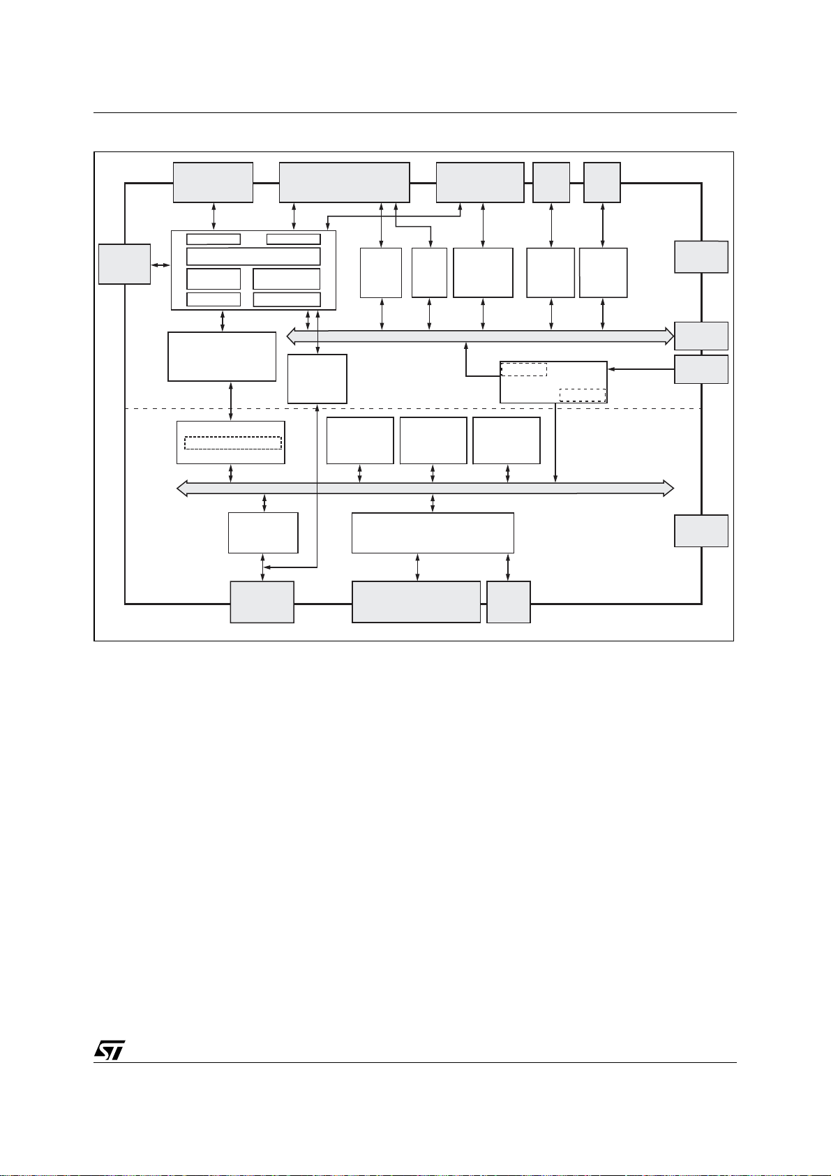
Figure 5. Functional Modules
uPSD34xx - HARDWARE DESCRIPTION
XTAL
Clock Unit
Die-to-Die Bus
8-Bit/16-Bit
Port 3 - UART0,
Intr, Timers
Turbo 8032 Core
Dual
UARTs
Inte rrupt
256 Byte SRAM
Dedicated Memory
Interface Prefetch,
Branch Cache
Enha nce d MCU Interface
PSD Page Register
Dec ode P LD
JTAG ISP
Port 1 - Timer, ADC, SPI
Port 1Port 3
3 Timer /
Counters
JTAG
DEBUG
Main Flash
10-bit
ADC
8032 Internal Bus
SPI
Secondary
Flash
PSD Interna l Bus
CPLD - 16 MACROCELLS
Port 4 - PCA,
PWM, UART1
PCA
PWM
Counters
Internal
Reset
SRAM
LVD
Reset Logic
Port 3
2
I
C
I2C
Unit
WDT
PSD
Reset
USB
pins
USB and
Trans-
ceiver
MCU Module
Reset Input
PSD Module
VCC Pins
3.3V
Ext.
Bus
Reset
Pin
VDD Pins
3.3V or 5V
uPSD34xx
Port C
JTAG and
GPIO
Port A,B,C PLD
I/O and GPIO
Port D
GPIO
AI10409
15/264

uPSD34xx - MEMORY ORGANIZATION
MEMORY ORGANIZATION
The 8032 MCU core views memory on the MCU
module as “internal” memory and it views memory
on the PSD module as “external” memory, see
Figure 6.
Internal memory on the MCU Module consists of
DATA, IDATA, and SFRs. These standard 8032
memories reside in 384 bytes of SRAM located at
a fixed address space starting at address 0x0000.
External memory on the PSD Module consists of
four types: main Flash (64K, 128K, or 256K bytes),
a smaller secondary Flash (32K), SRAM (4K or 8K
bytes), and a block of PSD Module control registers called csiop (256 bytes). These external memories reside at programmable address ranges,
specified using the software tool PSDsoft Express.
See the PSD Module section of this document for
more details on these memories.
External memory is accessed by the 8032 in two
separate 64K byte address spaces. One address
space is for program memory and the other ad-
Figure 6. uPSD34xx Memories
dress space is for data memory. Program memory
is accessed using the 8032 signal, PSEN
. Data
memory is accessed using the 8032 signals, RD
and WR. If the 8032 needs to access more than
64K bytes of external program or data memory, it
must use paging (or banking) techniques provided
by the Page Register in the PSD Module.
Note: When referencing program and data memory spaces, it has nothing to do with 8032 internal
SRAM areas of DATA, IDATA, and SFR on the
MCU Module. Program and data memory spaces
only relate to the external memories on the PSD
Module.
External memory on the PSD Module can overlap
the internal SRAM memory on the MCU Module in
the same physical address range (starting at
0x0000) without interference because the 8032
core does not assert the RD
or WR signals when
accessing internal SRAM.
Fixed
Addresses
FF
80
7F
0
Internal SRAM on
MCU Module
384 Bytes SRAM
Indirect
Addressing
I DATA
128 Bytes
128 Bytes
DATA
Direct or Indirect Addressing
SFR
128 Bytes
Direct
Addressing
Main
Flash
64KB
or
128KB
or
256KB
External Memory on
PSD Module
• External memories may be placed at virtually
any address using software tool PSDsoft Express.
• The SRAM and Flash memories may be placed
in 8032 Program Space or Data Space using
PSDsoft Express.
• Any memory in 8032 Data Space is XDATA.
Secondary
Flash
32KB
SRAM
4KB
or
8KB
AI10410
16/264

uPSD34xx - MEMORY ORGANIZATION
Internal Memory (MCU Module, Standard 8032
Memory: DATA, IDATA, SFR)
DATA Memory. The first 128 bytes of internal
SRAM ranging from address 0x0000 to 0x007F
are called DATA, which can be accessed using
8032 direct or indirect addressing schemes and
are typically used to store variables and stack.
Four register banks, each with 8 registers (R0 –
R7), occupy addresses 0x0000 to 0x001F. Only
one of these four banks may be enabled at a time.
The next 16 locations at 0x0020 to 0x002F contain
128 directly addressable bit locations that can be
used as software flags. SRAM locations 0x0030
and above may be used for variables and stack.
IDATA Memory. The next 128 bytes of internal
SRAM are named IDATA and range from address
0x0080 to 0x00FF. IDATA can be accessed only
through 8032 indirect addressing and is typically
used to hold the MCU stack as well as data variables. The stack can reside in both DATA and
IDATA memories and reach a size limited only by
the available space in the combined 256 bytes of
these two memories (since stack accesses are always done using indirect addressing, the boundary between DATA and IDATA does not exist with
regard to the stack).
SFR Memory. Special Function Registers (Table
5., page 25) occupy a separate physical memory,
but they logically overlap the same 128 bytes as
IDATA, ranging from address 0x0080 to 0x00FF.
SFRs are accessed only using direct addressing.
There 86 active registers used for many functions:
changing the operating mode of the 8032 MCU
core, controlling 8032 peripherals, controlling I/O,
and managing interrupt functions. The remaining
unused SFRs are reserved and should not be accessed.
16 of the SFRs are both byte- and bit-addressable.
Bit-addressable SFRs are those whose address
ends in “0” or “8” hex.
External Memory (PSD Module: Program
memory, Data memory)
The PSD Module has four memories: main Flash,
secondary Flash, SRAM, and csiop. See the PSD
MODULE section for more detailed information on
these memories.
Memory mapping in the PSD Module is implemented with the Decode PLD (DPLD) and optionally the Page Register. The user specifies decode
equations for individual segments of each of the
memories using the software tool PSDsoft Express. This is a very easy point-and-click process
allowing total flexibility in mapping memories. Additionally, each of the memories may be placed in
various combinations of 8032 program address
space or 8032 data address space by using the
software tool PSDsoft Express.
Program Memory. External program memory is
addressed by the 8032 using its 16-bit Program
Counter (PC) and is accessed with the 8032 signal, PSEN
any address in program space between 0x0000
and 0xFFFF.
After a power-up or reset, the 8032 begins program execution from location 0x0000 where the
reset vector is stored, causing a jump to an initialization routine in firmware. At address 0x0003, just
following the reset vector are the interrupt service
locations. Each interrupt is assigned a fixed interrupt service location in program memory. An interrupt causes the 8032 to jump to that service
location, where it commences execution of the
service routine. External Interrupt 0 (EXINT0), for
example, is assigned to service location 0x0003. If
EXINT0 is going to be used, its service routine
must begin at location 0x0003. Interrupt service locations are spaced at 8-byte intervals: 0x0003 for
EXINT0, 0x000B for Timer 0, 0x0013 for EXINT1,
and so forth. If an interrupt service routine is short
enough, it can reside entirely within the 8-byte interval. Longer service routines can use a jump instruction to somewhere else in program memory.
Data Memory. External data is referred to as
XDATA and is addressed by the 8032 using Indirect Addressing via its 16-bit Data Pointer Register
(DPTR) and is accessed by the 8032 signals, RD
and WR. XDATA can be present at any address in
data space between 0x0000 and 0xFFFF.
Note: the uPSD34xx has dual data pointers
(source and destination) making XDATA transfers
much more efficient.
Memory Placement. PSD Module architecture
allows the placement of its external memories into
different combinations of program memory and
data memory spaces. This means the main Flash,
the secondary Flash, and the SRAM can be
viewed by the 8032 MCU in various combinations
of program memory or data memory as defined by
PSDsoft Express.
As an example of this flexibility, for applications
that require a great deal of Flash memory in data
space (large lookup tables or extended data recording), the larger main Flash memory can be
placed in data space and the smaller secondary
Flash memory can be placed in program space.
The opposite can be realized for a different application if more Flash memory is needed for code
and less Flash memory for data.
. Program memory can be present at
17/264

uPSD34xx - 8032 MCU CORE PERFORMANCE ENHANCEMENTS
By default, the SRAM and csiop memories on the
PSD Module must always reside in data memory
space and they are treated by the 8032 as XDATA.
The main Flash and secondary Flash memories
may reside in program space, data space, or both.
These memory placement choices specified by
PSDsoft Express are programmed into non-volatile sections of the uPSD34xx, and are active at
power-up and after reset. It is possible to override
these initial settings during runtime for In-Application Programming (IAP).
Standard 8032 MCU architecture cannot write to
its own program memory space to prevent accidental corruption of firmware. However, this becomes an obstacle in typical 8032 systems when
a remote update to firmware in Flash memory is
required using IAP. The PSD module provides a
solution for remote updates by allowing 8032 firmware to temporarily “reclassify” Flash memory to
reside in data space during a remote update, then
returning Flash memory back to program space
when finished. See the VM Register (Table
104., page 174) in the PSD Module section of this
document for more details.
8032 MCU CORE PERFORMANCE ENHANCEMENTS
Before describing performance features of the
uPSD34xx, let us first look at standard 8032 architecture. The clock source for the 8032 MCU creates a basic unit of timing called a machine-cycle,
which is a period of 12 clocks for standard 8032
MCUs. The instruction set for traditional 8032
MCUs consists of 1, 2, and 3 byte instructions that
execute in different combinations of 1, 2, or 4 machine-cycles. For example, there are one-byte instructions that execute in one machine-cycle (12
clocks), one-byte instructions that execute in four
machine-cycles (48 clocks), two-byte, two-cycle
instructions (24 clocks), and so on. In addition,
standard 8032 architecture will fetch two bytes
from program memory on almost every machinecycle, regardless if it needs them or not (dummy
fetch). This means for one-byte, one-cycle instructions, the second byte is ignored. These one-byte,
one-cycle instructions account for half of the
8032's instructions (126 out of 255 opcodes).
There are inefficiencies due to wasted bus cycles
and idle bus times that can be eliminated.
The uPSD34xx 8032 MCU core offers increased
performance in a number of ways, while keeping
the exact same instruction set as the standard
8032 (all opcodes, the number of bytes per in-
struction, and the native number a machine-cycles
per instruction are identical to the original 8032).
The first way performance is boosted is by reducing the machine-cycle period to just 4 MCU clocks
as compared to 12 MCU clocks in a standard
8032. This shortened machine-cycle improves the
instruction rate for one- or two-byte, one-cycle instructions by a factor of three (Figure 7., page 19)
compared to standard 8051 architectures, and significantly improves performance of multiple-cycle
instruction types.
The example in Figure 7 shows a continuous execution stream of one- or two-byte, one-cycle instructions. The 5V uPSD34xx will yield 10 MIPS
peak performance in this case while operating at
40MHz clock rate. In a typical application however,
the effective performance will be lower since programs do not use only one-cycle instructions, but
special techniques are implemented in the
uPSD34xx to keep the effective MIPS rate as
close as possible to the peak MIPS rate at all
times. This is accomplished with an instruction
Pre-Fetch Queue (PFQ), a Branch Cache (BC),
and a 16-bit program memory bus as shown in
Figure 8., page 19.
18/264
uPSD34xx - 8032 MCU CORE PERFORMANCE ENHANCEMENTS
Figure 7. Comparison of uPSD34xx with Standard 8032 Performance
1- or 2-byte, 1-cycle Instructions
Instruction A Instruction B Instruction C
Turbo uPSD34xx
Execute Instruction and
Pre-Fetch Next Instruction
Execute Instruction and
Pre-Fetch Next Instruction
Execute Instruction and
Pre-Fetch Next Instruction
4 clocks (one machine cycle)
one machine cycle one machine cycle
MCU Clock
12 clocks (one machine cycle)
Instruction A
Standard 8032
Fetch Byte for Instruction A
Dummy Byte is Ignored (wasted bus access)
Turbo uPSD34xx executes instructions A, B, and C in the same
amount of time that a standard 8032 executes only Instruction A.
Figure 8. Instruction Pre-Fetch Queue and Branch Cache
Branch 4
Code
Branch
Cache
(BC)
Branch 3
Code
Branch 2
Code
Branch 4
Code
Branch 3
Code
Branch 1
Code
Compare
Branch 2
Code
Branch 1
Code
Execute Instruction A
and Fetch a Second Dummy Byte
AI10411
16-bit
Program
Memory
on PSD
Module
Instruction Byte
Instruction Byte
Address
Wait
Load on Branch Address Match
1616
8
8
4 Bytes of Instruction
16
Instruction Pre-Fetch Queue (PFQ)
Instruction Byte
Address
Wait
Current
Branch
Address
8
8032
MCU
16
AI10431
19/264

uPSD34xx - 8032 MCU CORE PERFORMANCE ENHANCEMENTS
Pre-Fetch Queue (PFQ) and Branch Cache
(BC)
The PFQ is always working to minimize the idle
bus time inherent to 8032 MCU architecture, to
eliminate wasted memory fetches, and to maximize memory bandwidth to the MCU. The PFQ
does this by running asynchronously in relation to
the MCU, looking ahead to pre-fetch two bytes
(word) of code from program memory during any
idle bus periods. Only necessary word will be
fetched (no dummy fetches like standard 8032).
The PFQ will queue up to four code bytes in advance of execution, which significantly optimizes
sequential program performance. However, when
program execution becomes non-sequential (program branch), a typical pre-fetch queue will empty
itself and reload new code, causing the MCU to
stall. The Turbo uPSD34xx diminishes this problem by using a Branch Cache with the PFQ. The
BC is a four-way, fully associative cache, meaning
that when a program branch occurs, its branch
destination address is compared simultaneously
with four recent previous branch destinations
stored in the BC. Each of the four cache entries
contain up to four bytes of code related to a
branch. If there is a hit (a match), then all four code
bytes of the matching program branch are transferred immediately and simultaneously from the
BC to the PFQ, and execution on that branch continues with minimal delay. This greatly reduces the
chance that the MCU will stall from an empty PFQ,
and improves performance in embedded control
systems where it is quite common to branch and
loop in relatively small code localities.
By default, the PFQ and BC are enabled after
power-up or reset. The 8032 can disable the PFQ
and BC at runtime if desired by writing to a specific
SFR (BUSCON).
The memory in the PSD module operates with
variable wait states depending on the value specified in the SFR named BUSCON. For example, a
5V uPSD34xx device operating at a 40MHz crystal
frequency requires four memory wait states (equal
to four MCU clocks). In this example, once the
PFQ has one word of code, the wait states become transparent and a full 10 MIPS is achieved
when the program stream consists of sequential
one- or two-byte, one machine-cycle instructions
as shown in Figure 7., page 19 (transparent because a machine-cycle is four MCU clocks which
equals the memory pre-fetch wait time that is also
four MCU clocks). But it is also important to understand PFQ operation on multi-cycle instructions.
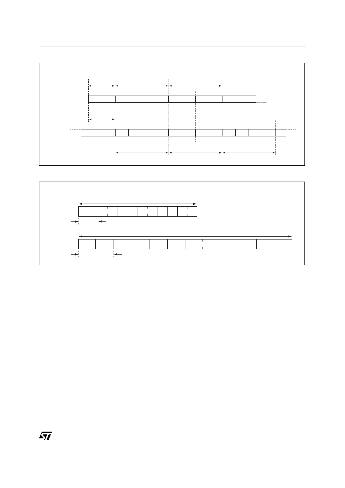
PFQ Example, Multi-cycle Instructions
Let us look at a string of two-byte, two-cycle instructions in Figure 9., page 21. There are three
instructions executed sequentially in this example,
instructions A, B, and C. Each of the time divisions
in the figure is one machine-cycle of four clocks,
and there are six phases to reference in this discussion. Each instruction is pre-fetched into the
PFQ in advance of execution by the MCU. Prior to
Phase 1, the PFQ has pre-fetched the two instruction bytes (A1 and A2) of Instruction A. During
Phase one, both bytes are loaded into the MCU
execution unit. Also in Phase 1, the PFQ is prefetching Instruction B (bytes B1 and B2) from program memory. In Phase 2, the MCU is processing
Instruction A internally while the PFQ is pre-fetching Instruction C. In Phase 3, both bytes of instruction B are loaded into the MCU execution unit and
the PFQ begins to pre-fetch bytes for the next instruction. In Phase 4 Instruction B is processed.
The uPSD34xx MCU instructions are an exact 1/3
scale of all standard 8032 instructions with regard
to number of cycles per instruction. Figure
10., page 21 shows the equivalent instruction se-
quence from the example above on a standard
8032 for comparison.
Aggregate Performance
The stream of two-byte, two-cycle instructions in
Figure 9., page 21, running on a 40MHz, 5V,
uPSD34xx will yield 5 MIPs. And we saw the
stream of one- or two-byte, one-cycle instructions
in Figure 7., page 19, on the same MCU yield 10
MIPs. Effective performance will depend on a
number of things: the MCU clock frequency; the
mixture of instructions types (bytes and cycles) in
the application; the amount of time an empty PFQ
stalls the MCU (mix of instruction types and misses on Branch Cache); and the operating voltage.
A 5V uPSD34xx device operates with four memory
wait states, but a 3.3V device operates with five
memory wait states yielding 8 MIPS peak compared to 10 MIPs peak for 5V device. The same
number of wait states will apply to both program
fetches and to data READ/WRITEs unless otherwise specified in the SFR named BUSCON.
In general, a 3X aggregate performance increase
is expected over any standard 8032 application
running at the same clock frequency.
20/264
uPSD34xx - 8032 MCU CORE PERFORMANCE ENHANCEMENTS
Figure 9. PFQ Operation on Multi-cycle Instructions
Three 2-byte, 2-cycle Instructions on uPSD34xx
Pre-Fetch
Inst A
Pre-Fetch Inst B and C Pre-Fetch next Inst
PFQ
MCU
Execution
Inst A, Byte 1&2 Inst B, Byte 1&2 Inst C, Byte 1&2 Next Inst
4-clock
Macine Cycle
Phase 1 Phase 2 Phase 3 Phase 4 Phase 6Phase 5
Previous Instruction A1 A2 Process A B1 B2 Process B C1 C2
Instruction A Instruction B Instruction C
Continue to Pre-Fetch
Figure 10. uPSD34xx Multi-cycle Instructions Compared to Standard 8032
Three 2-byte, 2-cycle Instructions, uPSD34xx vs. Standard 8032
24 Clocks Total (4 clocks per cycle)
uPSD34xx
Std 8032
A1
Byte 1
A2
Inst A
Byte 2
B1
1 Cycle
Process Inst A
B2
1 Cycle
Inst B
C1
C2
Inst C
72 Clocks (12 clocks per cycle)
Byte 1
Byte 2
Process Inst B
Byte 1
Byte 2
Process C
Process Inst C
Next Inst
AI10432
AI10412
21/264
uPSD34xx - MCU MODULE DISCRIPTION
MCU MODULE DISCRIPTION
This section provides a detail description of the
MCU Module system functions and peripherals, including:
■ 8032 MCU Registers
■ Special Function Registers
■ 8032 Addressing Modes
■ uPSD34xx Instruction Set Summary
■ Dual Data Pointers
■ Debug Unit
■ Interrupt System
■ MCU Clock Generation
■ Power Saving Modes
■ Oscillator and External Components
■ I/O Ports
8032 MCU REGISTERS
The uPSD34xx has the following 8032 MCU core
registers, also shown in Figure 11.
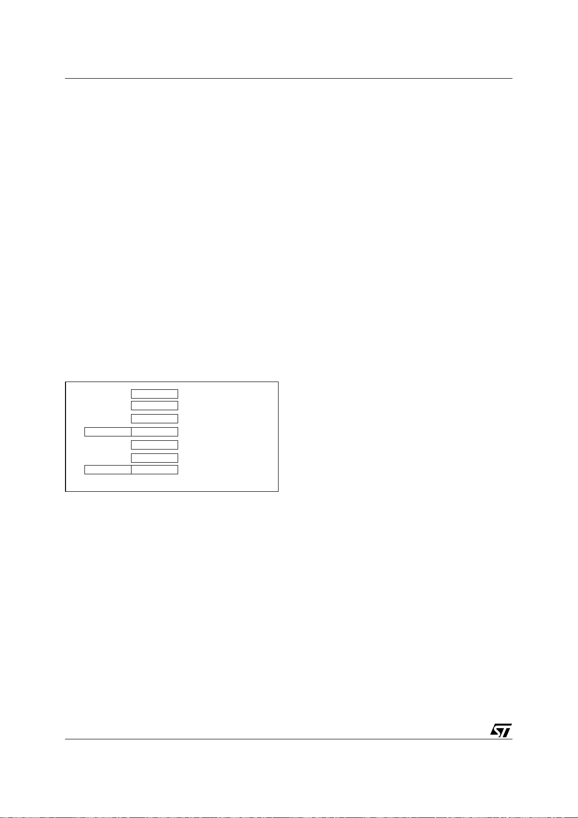
Figure 11. 8032 MCU Registers
A
B
SP
PCH
DPTR(DPH)
AI06636
PCL
PSW
R0-R7
DPTR(DPL)
Stack Pointer (SP)
The SP is an 8-bit register which holds the current
location of the top of the stack. It is incremented
before a value is pushed onto the stack, and decremented after a value is popped off the stack. The
SP is initialized to 07h after reset. This causes the
stack to begin at location 08h (top of stack). To
avoid overlapping conflicts, the user must initialize
the top of the stack to 20h if all four banks of registers R0 - R7 are used, as well as the top of stack
to 30h if all of the 8032 bit memory locations are
used.
Data Pointer (DPTR)
DPTR is a 16-bit register consisting of two 8-bit
registers, DPL and DPH. The DPTR Register is
used as a base register to create an address for indirect jumps, table look-up operations, and for external data transfers (XDATA). When not used for
Accumulator
B Register
Stack Pointer
Program Counter
Program Status Word
General Purpose
Register (Bank0-3)
Data Pointer Register
■ MCU Bus Interface
■ Supervisory Functions
■ Standard 8032 Timer/Counters
■ Serial UART Interfaces
■ IrDA Interface
2
■ I
C Interface
■ SPI Interface
■ Analog to Digital Converter
■ Programmable Counter Array (PCA)
■ USB Interface
Note: A full description of the 8032 instruction set
may be found in the uPSD34xx Programmers
Guide.
addressing, the DPTR Register can be used as a
general purpose 16-bit data register.
Very frequently, the DPTR Register is used to access XDATA using the External Direct addressing
mode. The uPSD34xx has a special set of SFR
registers (DPTC, DPTM) to control a secondary
DPTR Register to speed memory-to-memory
XDATA transfers. Having dual DPTR Registers allows rapid switching between source and destination addresses (see details in DUAL DATA
POINTERS, page 38).
Program Counter (PC)
The PC is a 16-bit register consisting of two 8-bit
registers, PCL and PCH. This counter indicates
the address of the next instruction in program
memory to be fetched and executed. A reset forces the PC to location 0000h, which is where the reset jump vector is stored.
Accumulator (ACC)
This is an 8-bit general purpose register which
holds a source operand and receives the result of
arithmetic operations. The ACC Register can also
be the source or destination of logic and data
movement operations. For MUL and DIV instructions, ACC is combined with the B Register to hold
16-bit operands. The ACC is referred to as “A” in
the MCU instruction set.
B Register (B)
The B Register is a general purpose 8-bit register
for temporary data storage and also used as a 16bit register when concatenated with the ACC Register for use with MUL and DIV instructions.
22/264
General Purpose Registers (R0 - R7)
There are four banks of eight general purpose 8bit registers (R0 - R7), but only one bank of eight
registers is active at any given time depending on
the setting in the PSW word (described next). R0 R7 are generally used to assist in manipulating
values and moving data from one memory location
to another. These register banks physically reside
in the first 32 locations of 8032 internal DATA
SRAM, starting at address 00h. At reset, only the
first bank of eight registers is active (addresses
00h to 07h), and the stack begins at address 08h.
Program Status Word (PSW)
The PSW is an 8-bit register which stores several
important bits, or flags, that are set and cleared by
many 8032 instructions, reflecting the current
state of the MCU core. Figure 12., page 23 shows
the individual flags.
Carry Flag (CY). This flag is set when the last
arithmetic operation that was executed results in a
carry (addition) or borrow (subtraction). It is
cleared by all other arithmetic operations. The CY
flag is also affected by Shift and Rotate Instructions.
Auxiliary Carry Flag (AC). This flag is set when
the last arithmetic operation that was executed results in a carry into (addition) or borrow from (subtraction) the high-order nibble. It is cleared by all
other arithmetic operations.
uPSD34xx - 8032 MCU REGISTERS
General Purpose Flag (F0). This is a bit-addres-
sable, general-purpose flag for use under software
control.
Register Bank Select Flags (RS1, RS0). These
bits select which bank of eight registers is used
during R0 - R7 register accesses (see Table 4)
Overflow Flag (OV). The OV flag is set when: an
ADD, ADDC, or SUBB instruction causes a sign
change; a MUL instruction results in an overflow
(result greater than 255); a DIV instruction causes
a divide-by-zero condition. The OV flag is cleared
by the ADD, ADDC, SUBB, MUL, and DIV instructions in all other cases. The CLRV instruction will
clear the OV flag at any time.
Parity Flag (P). The P flag is set if the sum of the
eight bits in the Accumulator is odd, and P is
cleared if the sum is even.
Table 4. .Register Bank Select Addresses
RS1 RS0
0 0 0 00h - 07h
0 1 1 08h - 0Fh
1 0 2 10h - 17h
1 1 3 18h - 1Fh
Register
Bank
8032 Internal
DATA Address
Figure 12. Program Status Word (PSW) Register
MSB
CY
PSW
Carry Flag
Auxillary Carry Flag
General Purpose Flag
AC FO RS1 RS0 OV P
Register Bank Select Flags
(to select Bank0-3)
LSB
Reset Value 00h
Parity Flag
Bit not assigned
Overflow Flag
AI06639
23/264

uPSD34xx - SPECIAL FUNCTION REGISTERS (SFR)
SPECIAL FUNCTION REGISTERS (SFR)
A group of registers designated as Special Function Register (SFR) is shown in Table 5., page 25.
SFRs control the operating modes of the MCU
core and also control the peripheral interfaces and
I/O pins on the MCU Module. The SFRs can be accessed only by using the Direct Addressing method within the address range from 80h to FFh of
internal 8032 SRAM. Sixteen addresses in SFR
address space are both byte- and bit-addressable.
The bit-addressable SFRs are noted in Table 5.
106 of a possible 128 SFR addresses are occupied. The remaining unoccupied SFR addresses
(designated as “RESERVED” in Table 5) should
not be written. Reading unoccupied locations will
return an undefined value.
Note: There is a separate set of control registers
for the PSD Module, designated as csiop, and they
are described in the PSD MODULE, page 164.
The I/O pins, PLD, and other functions on the PSD
Module are NOT controlled by SFRs.
SFRs are categorized as follows:
■ MCU core registers:
IP, A, B, PSW, SP, DPTL, DPTH, DPTC,
DPTM
■ MCU Module I/O Port registers:
P1, P3, P4, P1SFS0, P1SFS1, P3SFS,
P4SFS0, P4SFS1
■ Standard 8032 Timer registers
TCON, TMOD, T2CON, TH0, TH1, TH2, TL0,
TL1, TL2, RCAP2L, RCAP2H
■ Standard Serial Interfaces (UART)
SCON0, SBUF0, SCON1, SBUF1
■ Power, clock, and bus timing registers
PCON, CCON0, CCON1, BUSCON
■ Hardware watchdog timer registers
WDKEY, WDRST
■ Interrupt system registers
IP, IPA, IE, IEA
■ Prog. Counter Array (PCA) control
registers
PCACL0, PCACH0, PCACON0, PCASTA,
PCACL1, PCACH1, PCACON1, CCON2,
CCON3
■ PCA capture/compare and PWM registers
CAPCOML0, CAPCOMH0, TCMMODE0,
CAPCOML1, CAPCOMH1, TCMMODE2,
CAPCOML2, CAPCOMH2, TCMMODE2,
CAPCOML3, CAPCOMH3, TCMMODE3,
CAPCOML4, CAPCOMH4, TCMMODE4,
CAPCOML5, CAPCOMH5, TCMMODE5,
PWMF0, PMWF1
■ SPI interface registers
SPICLKD, SPISTAT, SPITDR, SPIRDR,
SPICON0, SPICON1
2
■ I
C interface registers
S1SETUP, S1CON, S1STA, S1DAT, S1ADR
■ Analog to Digital Converter registers
ACON, ADCPS, ADAT0, ADAT1
■ IrDA interface register
IRDACON
■ USB interface registers
UADDR, UPAIR, WE0-3, UIF0-3, UCTL,
USTA, USEL, UCON, USIZE, UBASEH,
UBASEL, USCI, USCV
24/264
uPSD34xx - SPECIAL FUNCTION REGISTERS (SFR)
Table 5. SFR Memory Map with Direct Address and Reset Value
SFR
Addr
(hex)
80 RESERVED
81 SP SP[7:0] 07
82 DPL DPL[7:0] 00 Data
83 DPH DPH[7:0] 00
84 RESERVED
85 DPTC – AT – – – DPSEL[2:0] 00
86 DPTM – – – – MD1[1:0] MD0[1:0] 00
87 PCON SMOD0 SMOD1 – POR RCLK1 TCLK1 PD IDLE 00
88
89 TMOD GATE C/T
8A TL0 TL0[7:0] 00
8B TL1 TL1[7:0] 00
8C TH0 TH0[7:0] 00
8D TH1 TH1[7:0] 00
8E P1SFS0 P1SFS0[7:0] 00
8F P1SFS1 P1SFS1[7:0] 00
90
91 P3SFS P3SFS[7:0] 00
92 P4SFS0 P4SFS0[7:0] 00
93 P4SFS1 P4SFS1[7:0] 00
(1)
(1)
SFR
Name
TCON
P1
76 5 43210
TF1
<8Fh>
P1.7
<97h>
TR1
<8Eh>
P1.6
<96h>
Bit Name and <Bit Address> Reset
TF0
<8Dh>
M1 M0 GATE C/T M1 M0 00
P1.5
<95h>
TR0
<8Ch>
P1.4
<94h>
IE1
<8Bh>
P1.3
<93h>
IT1
<8Ah>
P1.2
<92h>
IE0
<89h>
P1.1
<91h>
IT0
<88h>
P1.0
<90h>
Value
(hex)
00
FF
with Link
Pointer
(SP), page
Pointer
(DPTR), p
age 22
13., page
14., page
26., page
41., page
42., page
Standard
SFRs, pag
31., page
32., page
27., page
30., page
34., page
35., page
Reg.
Descr.
Stack
22
Table
38
Table
39
Table
52
Table
72
Table
74
Timer
e71
Table
61
Table
61
Table
58
Table
61
Table
62
Table
62
25/264
uPSD34xx - SPECIAL FUNCTION REGISTERS (SFR)
SFR
Addr
(hex)
94 ADCPS – – – – ADCCE ADCPS[2:0] 00
95 ADAT0 ADATA[7:0] 00
96 ADAT1 – – – – – – ADATA[9:8] 00
97 ACON AINTF AINTEN ADEN ADS[2:0] ADST ADSF 00
98
99 SBUF0 SBUF0[7:0] 00
9A RESERVED
9B RESERVED
9C RESERVED
9D BUSCON EPFQ EBC WRW1 WRW0 RDW1 RDW0 CW1 CW0 EB
9E RESERVED
9F RESERVED
A0 RESERVED
A1 RESERVED
A2 PCACL0 PCACL0[7:0] 00
A3 PCACH0 PCACH0[7:0] 00
A4 PCACON0 EN_ALL EN_PCA EOVF1 PCA_IDL – – CLK_SEL[1:0] 00
A5 PCASTA OVF1 INTF5 INTF4 INTF3 OVF0 INTF2 INTF1 INTF0 00
A6 WDRST WDRST[7:0] 00
A7 IEA EADC ESPI EPCA ES1 – – EI2C – 00
(1)
SFR
Name
SCON0
76 5 43210
SM0
<9Fh>
SM1
<9Eh>
Bit Name and <Bit Address> Reset
SM2
<9Dh>
REN
<9Ch>
TB8
<9Bh>
RB8
<9Ah>TI<99h>RI<9h8>
Value
(hex)
00
Reg.
Descr.
with Link
Table
90., page
153
Table
91., page
153
Table
92., page
153
Table
89., page
152
Table
47., page
84
Figure
28., page
81
Table
37., page
65
Table
93., page
155
Table
93., page
155
Table
96., page
160
Table
98., page
162
Table
40., page
70
Table
18., page
45
26/264
uPSD34xx - SPECIAL FUNCTION REGISTERS (SFR)
SFR
Addr
(hex)
(1)
A8
A9
AA
AB
AC
AD
SFR
Name
IE
TCMMODE
0
TCMMODE
1
TCMMODE
2
CAPCOML
0
CAPCOMH
0
76 5 43210
EA
<AFh>
–
EINTF E_COMP CAP_PE CAP_NE MATCH TOGGLE PWM[1:0] 00
EINTF E_COMP CAP_PE CAP_NE MATCH TOGGLE PWM[1:0] 00
EINTF E_COMP CAP_PE CAP_NE MATCH TOGGLE PWM[1:0] 00
Bit Name and <Bit Address> Reset
ET2
<ADh>
ES0
<ACh>
ET1
<ABh>
EX1
<AAh>
ET0
<A9h>
EX0
<A8h>
CAPCOML0[7:0] 00
CAPCOMH0[7:0] 00
Value
(hex)
00
Reg.
Descr.
with Link
Table
17., page
45
Table
99., page
163
Table
93., page
155
Table
AE WDKEY WDKEY[7:0] 55
39., page
70
Table
93., page
155
Table
28., page
59
Table
93., page
155
B0
AF
(1)
B1
B2
B3
CAPCOML
1
P3
CAPCOMH
1
CAPCOML
2
CAPCOMH
2
P3.7
<B7h>
P3.6
<B6h>
P3.5
<B5h>
CAPCOML1[7:0] 00
P3.4
<B4h>
P3.3
<B3h>
P3.2
<B2h>
P3.1
<B1h>
P3.0
<B0h>
FF
CAPCOMH1[7:0] 00
CAPCOML2[7:0] 00
CAPCOMH2[7:0] 00
B4 PWMF0 PWMF0[7:0] 00
B5 RESERVED
B6 RESERVED
Table
B7 IPA PADC PSPI PPCA PS1 – – PI2C – 00
20., page
46
Table
19., page
46
B8
(1)
IP – –
PT2
<BDh>
PS0
<BCh>
PT1
<BBh>
PX1
<BAh>
PT0
<B9h>
PX0
<B8h>
00
B9 RESERVED
BA PCACL1 PCACL1[7:0] 00 Table
BB PCACH1 PCACH1[7:0] 00
93., page
155
Table
BC PCACON1 – EN_PCA EOVF1 PCA_IDL – – CLK_SEL[1:0] 00
97., page
161
27/264

uPSD34xx - SPECIAL FUNCTION REGISTERS (SFR)
SFR
Addr
(hex)
BD
BE
BF
(1)
C0
C1
C2
C3
C4
C5
C6
SFR
Name
TCMMODE
3
TCMMODE
4
TCMMODE
5
P4
CAPCOML
3
CAPCOMH
3
CAPCOML
4
CAPCOMH
4
CAPCOML
5
CAPCOMH
5
76 5 43210
EINTF E_COMP CAP_PE CAP_NE MATCH TOGGLE PWM[1:0] 00
EINTF E_COMP CAP_PE CAP_NE MATCH TOGGLE PWM[1:0] 00
EINTF E_COMP CAP_PE CAP_NE MATCH TOGGLE PWM[1:0] 00
P4.7
<C7h>
P4.6
<C6h>
Bit Name and <Bit Address> Reset
P4.5
<C5h>
P4.4
<C4h>
P4.3
<C3h>
P4.2
<C2h>
P4.1
<C1h>
P4.0
<C0h>
CAPCOML3[7:0] 00
CAPCOMH3[7:0] 00
CAPCOML4[7:0] 00
CAPCOMH4[7:0] 00
CAPCOML5[7:0] 00
CAPCOMH5[7:0] 00
C7 PWMF1 PWMF1[7:0] 00
CP/
RL2
<C8h>
C8
(1)
T2CON
TF2
<CFh>
EXF2
<CEh>
RCLK
<CDh>
TCLK
<CCh>
EXEN2
<CBh>
TR2
<CAh>
C/T2
<C9h>
C9 RESERVED
CA RCAP2L RCAP2L[7:0] 00
CB RCAP2H RCAP2H[7:0] 00
CC TL2 TL2[7:0] 00
CD TH2 TH2[7:0] 00
CE IRDACON – IRDA_EN BIT_PULS CDIV4 CDIV3 CDIV2 CDIV1 CDIV0 0F
D0
(1)
PSW
CY
<D7h>AC<D6h>F0<D5h>
RS[1:0]
<D4h, D3h>
OV
<D2h>
–
P
<D0>
D1 RESERVED
D2 SPICLKD SPICLKD[5:0] – – 04
D3 SPISTAT – – – BUSY TEISF RORISF TISF RISF 02
Value
(hex)
FF
00
00
Reg.
Descr.
with Link
Table
99., page
163
Table
29., page
59
Table
93., page
155
Table
43., page
77
Standard
Timer
SFRs, pag
e71
Table
50., page
95
Program
Status
Word
(PSW), pa
ge 23
Table
65., page
121
Table
66., page
122
28/264

uPSD34xx - SPECIAL FUNCTION REGISTERS (SFR)
SFR
Addr
(hex)
SFR
Name
76 5 43210
Bit Name and <Bit Address> Reset
Value
(hex)
Reg.
Descr.
with Link
D4 SPITDR SPITDR[7:0] 00 Table
D5 SPIRDR SPIRDR[7:0] 00
64., page
121
Table
D6 SPICON0 – TE RE SPIEN SSEL FLSB SPO – 00
63., page
120
Table
D7 SPICON1 – – – – TEIE RORIE TIE RIE 00
64., page
121
Table
48., page
85
D8
(1)
SCON1
SM0
<DF
SM1
<DE>
SM2
<DD>
REN
<DC>
TB8
<DB>
RB8
<DA>TI<D9>RI<D8>
00
Figure
D9 SBUF1 SBUF1[7:0] 00
28., page
81
DA RESERVED
Table
DB S1SETUP SS_EN SMPL_SET[6:0] 00
59., page
108
Table
DC S1CON CR2 EN1 STA STO ADDR AA CR1 CR0 00
54., page
103
Table
DD S1STA GC STOP INTR TX_MD B_BUSY B_LOST ACK_R
SLV 00
56., page
106
Table
DE S1DAT S1DAT[7:0] 00
57., page
107
Table
DF S1ADR S1ADR[7:0] 00
58., page
107
Accumulat
E0
(1)
A
<bit addresses: E7h, E6h, E5h, E4h, E3h, E2h, E1h, E0h>
A[7:0]
00
(ACC), pa
ge 22
E1 RESERVED
E2 UADDR – USBADDR[6:0] 00
E3 UPAIR – – – – PR3OUT PR1OUT PR3IN PR1IN 00
E4 UIE0 – – – – RSTIE
SUSPND
IE
EOPIE
RES
UMIE
00
E5 UIE1 – – – IN4IE IN3IE IN2IE IN1IE IN0IE 00
E6 UIE2 – – – OUT4IE OUT3IE OUT2IE OUT1IE
E7 UIE3 – – – NAK4IE NAK3IE NAK2IE NAK1IE
E8 UIF0 GLF INF OUTF NAKF RSTF
SUSPND
F
EOPF
OUT0I
E
NAK0I
E
RESU
MF
00
00
00
or
29/264
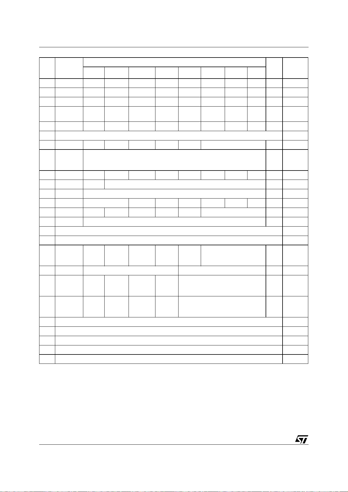
uPSD34xx - SPECIAL FUNCTION REGISTERS (SFR)
SFR
Addr
(hex)
SFR
Name
76 5 43210
Bit Name and <Bit Address> Reset
Value
(hex)
with Link
E9 UIF1 – – – IN4F IN3F IN2F IN1F IN0F 00
EA UIF2 – – – OUT4F OUT3F OUT2F OUT1F OUT0F 00
EB UIF3 – – – NAK4F NAK3F NAK2F NAK1F NAK0F 00
EC UCTL – – – – – USBEN VISIBLE
WAKE
UP
00
ED USTA – – – – RCVT SETUP IN OUT 00
EE RESERVED
EF USEL DIR – – – – EP[2:0] 00
F0
(1)
B
<bit addresses: F7h, F6h, F5h, F4h, F3h, F2h, F1h, F0h>
B[7:0]
00
B Register
(B), page
F1 UCON – – – – ENABLE STALL TOGGLE BSY 00
F2 USIZE – SIZE[6:0] 00
F3 UBASEH BASEADDR[15:8] 00
F4 UBASEL BASEADDR[7:6] 0 0 0 0 0 0 00
F5 USCI – – – – – USCI[2:0] 00
F6 USCV USCV[7:0] 00
F7 RESERVED
F8 RESERVED
F9 CCON0 PLLM[4] PLLEN UPLLCE DBGCE
CPU_
AR
CPUPS[2:0] 50
22., page
FA CCON1 PLLM[3:0] PLLD[3:0] 00
FB CCON2 – – – PCA0CE PCA0PS[3:0] 10
FC CCON3 – – – PCA1CE PCA1PS[3:0] 10
94., page
95., page
FD RESERVED
FE RESERVED
FF RESERVED
FE RESERVED
FF RESERVED
Note: 1. This SFR can be addressed by individual bits (Bit Address mode) or addressed by the entire byte (Direct Address mode).
Reg.
Descr.
22
Table
49
Table
156
Table
156
30/264
 Loading...