

ST uPSD3422E-40T6, uPSD3422EV-40T6, uPSD3422E-40U6, uPSD3422EV-40U6, uPSD3433E-40T6 User Manual
...
查询UPSD3422供应商
Fast Turbo 8032 MCU with USB and Programmable Logic
FEATURES SUMMARY
■ FAST 8-BIT TURBO 8032 MCU, 40MHz
– Advanced core, 4-clocks per instruction
– 10 MIPs peak performance at 40MHz (5V)
– JTAG Debug and In-System
Programming
– 16-bit internal instruction path fetches
double-byte instruction in a single memory
cycle
– Branch Cache & 4 instruction Prefetch
Queue
– Dual XDATA pointers with automatic
increment and decrement
– Compatible with 3rd party 8051 tools
■ DUAL FLASH MEMORIES WITH MEMORY
MANAGEMENT
– Place either memory into 8032 program
address space or data address space
– READ-while-WRITE operation for In-
Application Programming and EEPROM
emulation
– Single voltage program and erase
– 100K guaranteed erase cycles, 15-year
retention
■ CLOCK, RESET, AND POWER SUPPLY
MANAGEMENT
– SRAM is Battery Backup capable
– Flexible 8-level CPU clock divider register
– Normal, Idle, and Power Down Modes
– Power-on and Low Voltage reset
supervisor
– Programmable Watchdog Timer
■ PROGRAMMABLE LOGIC, GENERAL
PURPOSE
– 16 macrocells for logic applications (e.g.,
shifters, state machines, chip-selects,
glue-logic to keypads, and LCDs)
■ A/D CONVERTER
– Eight Channels, 10-bit resolution, 6µs
uPSD34xx
Turbo Plus Series
PRELIMINARY DATA
Figure 1. Packages
TQFP52 (T), 52-lead, Thin, Quad, Flat
TQFP80 (U), 80-lead, Thin, Quad, Flat
■ COMMUNICATION INTERFACES
– USB v2.0 Full Speed (12Mbps)
10 endpoint pairs (In/Out), each endpoint
with 64-byte FIFO (supports Control, Intr,
and Bulk transfer types)
2
C Master/Slave controller, 833kHz
–I
– SPI Master controller, 1MHz
– Two UARTs with independent baud rate
– IrDA Potocol: up to 115 kbaud
– Up to 46 I/O, 5V tolerant uPSD34xxV
■ TIMERS AND INTERRUPTS
– Three 8032 standard 16-bit timers
– Programmable Counter Array (PCA), six
16-bit modules for PWM, CAPCOM, and
timers
– 8/10/16-bit PWM operation
– 12 Interrupt sources with two external
interrupt pins
■ OPERATING VOLTAGE SOURCE (±10%)
– 5V Devices: 5.0V and 3.3V sources
– 3.3V Devices: 3.3V source
Rev 2.0
March 2005
This is preliminary information on a new product now in development or undergoing evaluation. Details are subject to change without notice.
1/264
uPSD34xx - FEATURES SUMMARY
Table 1. Device Summary
1st
Part Number Max MHz
Flash
(bytes)
uPSD3422E-40T6 40 64K 32K 4K 35 No 3.3V 5.0V TQFP52
uPSD3422EV-40T6 40 64K 32K 4K 35 No 3.3V 3.3V TQFP52
uPSD3422E-40U6 40 64K 32K 4K 46 Yes 3.3V 5.0V TQFP80
uPSD3422EV-40U6 40 64K 32K 4K 46 Yes 3.3V 3.3V TQFP80
uPSD3433E-40T6 40 128K 32K 8K 35 No 3.3V 5.0V TQFP52
uPSD3433EV-40T6 40 128K 32K 8K 35 No 3.3V 3.3V TQFP52
uPSD3433E-40U6 40 128K 32K 8K 46 Yes 3.3V 5.0V TQFP80
uPSD3433EV-40U6 40 128K 32K 8K 46 Yes 3.3V 3.3V TQFP80
uPSD3434E-40T6 40 256K 32K 8K 35 No 3.3V 5.0V TQFP52
uPSD3434EV-40T6 40 256K 32K 8K 35 No 3.3V 3.3V TQFP52
uPSD3434E-40U6 40 256K 32K 8K 46 Yes 3.3V 5.0V TQFP80
uPSD3434EV-40U6 40 256K 32K 8K 46 Yes 3.3V 3.3V TQFP80
Note: Operating temperature is in the Industrial range (–40°C to 85°C).
2nd
Flash
SRAM GPIO
8032
Bus
V
CC
V
DD
Pkg.
2/264

uPSD34xx - TABLE OF CONTENTS
TABLE OF CONTENTS
FEATURES SUMMARY . . . . . . . . . . . . . . . . . . . . . . . . . . . . . . . . . . . . . . . . . . . . . . . . . . . . . . . . . . . . . 1
TABLE OF CONTENTS . . . . . . . . . . . . . . . . . . . . . . . . . . . . . . . . . . . . . . . . . . . . . . . . . . . . . . . . . . . . . 3
SUMMARY DESCRIPTION . . . . . . . . . . . . . . . . . . . . . . . . . . . . . . . . . . . . . . . . . . . . . . . . . . . . . . . . . . . 7
PIN DESCRIPTIONS . . . . . . . . . . . . . . . . . . . . . . . . . . . . . . . . . . . . . . . . . . . . . . . . . . . . . . . . . . . . . . . . 9
HARDWARE DESCRIPTION . . . . . . . . . . . . . . . . . . . . . . . . . . . . . . . . . . . . . . . . . . . . . . . . . . . . . . . . 14
MEMORY ORGANIZATION . . . . . . . . . . . . . . . . . . . . . . . . . . . . . . . . . . . . . . . . . . . . . . . . . . . . . . . . . 16
Internal Memory (MCU Module, Standard 8032 Memory: DATA, IDATA, SFR) . . . . . . . . . . . . 17
External Memory (PSD Module: Program memory, Data memory). . . . . . . . . . . . . . . . . . . . . . 17
8032 MCU CORE PERFORMANCE ENHANCEMENTS . . . . . . . . . . . . . . . . . . . . . . . . . . . . . . . . . . . 18
Pre-Fetch Queue (PFQ) and Branch Cache (BC) . . . . . . . . . . . . . . . . . . . . . . . . . . . . . . . . . . . . 20
PFQ Example, Multi-cycle Instructions . . . . . . . . . . . . . . . . . . . . . . . . . . . . . . . . . . . . . . . . . . . . 20
Aggregate Performance . . . . . . . . . . . . . . . . . . . . . . . . . . . . . . . . . . . . . . . . . . . . . . . . . . . . . . . . 20
MCU MODULE DISCRIPTION . . . . . . . . . . . . . . . . . . . . . . . . . . . . . . . . . . . . . . . . . . . . . . . . . . . . . . . 22
8032 MCU REGISTERS . . . . . . . . . . . . . . . . . . . . . . . . . . . . . . . . . . . . . . . . . . . . . . . . . . . . . . . . . . . . 22
Stack Pointer (SP) . . . . . . . . . . . . . . . . . . . . . . . . . . . . . . . . . . . . . . . . . . . . . . . . . . . . . . . . . . . . . 22
Data Pointer (DPTR) . . . . . . . . . . . . . . . . . . . . . . . . . . . . . . . . . . . . . . . . . . . . . . . . . . . . . . . . . . . 22
Program Counter (PC). . . . . . . . . . . . . . . . . . . . . . . . . . . . . . . . . . . . . . . . . . . . . . . . . . . . . . . . . . 22
Accumulator (ACC) . . . . . . . . . . . . . . . . . . . . . . . . . . . . . . . . . . . . . . . . . . . . . . . . . . . . . . . . . . . . 22
B Register (B). . . . . . . . . . . . . . . . . . . . . . . . . . . . . . . . . . . . . . . . . . . . . . . . . . . . . . . . . . . . . . . . . 22
General Purpose Registers (R0 - R7). . . . . . . . . . . . . . . . . . . . . . . . . . . . . . . . . . . . . . . . . . . . . . 23
Program Status Word (PSW) . . . . . . . . . . . . . . . . . . . . . . . . . . . . . . . . . . . . . . . . . . . . . . . . . . . .23
SPECIAL FUNCTION REGISTERS (SFR) . . . . . . . . . . . . . . . . . . . . . . . . . . . . . . . . . . . . . . . . . . . . . . 24
8032 ADDRESSING MODES . . . . . . . . . . . . . . . . . . . . . . . . . . . . . . . . . . . . . . . . . . . . . . . . . . . . . . . . 31
Register Addressing . . . . . . . . . . . . . . . . . . . . . . . . . . . . . . . . . . . . . . . . . . . . . . . . . . . . . . . . . . . 31
Direct Addressing . . . . . . . . . . . . . . . . . . . . . . . . . . . . . . . . . . . . . . . . . . . . . . . . . . . . . . . . . . . . . 31
Register Indirect Addressing . . . . . . . . . . . . . . . . . . . . . . . . . . . . . . . . . . . . . . . . . . . . . . . . . . . . 31
Immediate Addressing . . . . . . . . . . . . . . . . . . . . . . . . . . . . . . . . . . . . . . . . . . . . . . . . . . . . . . . . . 31
External Direct Addressing . . . . . . . . . . . . . . . . . . . . . . . . . . . . . . . . . . . . . . . . . . . . . . . . . . . . . 31
External Indirect Addressing . . . . . . . . . . . . . . . . . . . . . . . . . . . . . . . . . . . . . . . . . . . . . . . . . . . . 31
Indexed Addressing . . . . . . . . . . . . . . . . . . . . . . . . . . . . . . . . . . . . . . . . . . . . . . . . . . . . . . . . . . . 32
Relative Addressing . . . . . . . . . . . . . . . . . . . . . . . . . . . . . . . . . . . . . . . . . . . . . . . . . . . . . . . . . . . 32
Absolute Addressing . . . . . . . . . . . . . . . . . . . . . . . . . . . . . . . . . . . . . . . . . . . . . . . . . . . . . . . . . . 32
Long Addressing . . . . . . . . . . . . . . . . . . . . . . . . . . . . . . . . . . . . . . . . . . . . . . . . . . . . . . . . . . . . . . 32
Bit Addressing . . . . . . . . . . . . . . . . . . . . . . . . . . . . . . . . . . . . . . . . . . . . . . . . . . . . . . . . . . . . . . . . 32
3/264

uPSD34xx - TABLE OF CONTENTS
uPSD34xx INSTRUCTION SET SUMMARY . . . . . . . . . . . . . . . . . . . . . . . . . . . . . . . . . . . . . . . . . . . . 33
DUAL DATA POINTERS. . . . . . . . . . . . . . . . . . . . . . . . . . . . . . . . . . . . . . . . . . . . . . . . . . . . . . . . . . . . 38
Data Pointer Control Register, DPTC (85h) . . . . . . . . . . . . . . . . . . . . . . . . . . . . . . . . . . . . . . . . . 38
Data Pointer Mode Register, DPTM (86h) . . . . . . . . . . . . . . . . . . . . . . . . . . . . . . . . . . . . . . . . . . 39
DEBUG UNIT. . . . . . . . . . . . . . . . . . . . . . . . . . . . . . . . . . . . . . . . . . . . . . . . . . . . . . . . . . . . . . . . . . . . . 40
INTERRUPT SYSTEM. . . . . . . . . . . . . . . . . . . . . . . . . . . . . . . . . . . . . . . . . . . . . . . . . . . . . . . . . . . . . . 41
Individual Interrupt Sources . . . . . . . . . . . . . . . . . . . . . . . . . . . . . . . . . . . . . . . . . . . . . . . . . . . . . 44
MCU CLOCK GENERATION . . . . . . . . . . . . . . . . . . . . . . . . . . . . . . . . . . . . . . . . . . . . . . . . . . . . . . . . 47
MCU_CLK . . . . . . . . . . . . . . . . . . . . . . . . . . . . . . . . . . . . . . . . . . . . . . . . . . . . . . . . . . . . . . . . . . . . 47
PERIPH_CLK . . . . . . . . . . . . . . . . . . . . . . . . . . . . . . . . . . . . . . . . . . . . . . . . . . . . . . . . . . . . . . . . . 47
POWER SAVING MODES . . . . . . . . . . . . . . . . . . . . . . . . . . . . . . . . . . . . . . . . . . . . . . . . . . . . . . . . . . 50
Idle Mode . . . . . . . . . . . . . . . . . . . . . . . . . . . . . . . . . . . . . . . . . . . . . . . . . . . . . . . . . . . . . . . . . . . . 50
Power-down Mode. . . . . . . . . . . . . . . . . . . . . . . . . . . . . . . . . . . . . . . . . . . . . . . . . . . . . . . . . . . . . 50
Reduced Frequency Mode . . . . . . . . . . . . . . . . . . . . . . . . . . . . . . . . . . . . . . . . . . . . . . . . . . . . . . 50
OSCILLATOR AND EXTERNAL COMPONENTS . . . . . . . . . . . . . . . . . . . . . . . . . . . . . . . . . . . . . . . . 53
I/O PORTS of MCU MODULE. . . . . . . . . . . . . . . . . . . . . . . . . . . . . . . . . . . . . . . . . . . . . . . . . . . . . . . . 54
MCU Port Operating Modes . . . . . . . . . . . . . . . . . . . . . . . . . . . . . . . . . . . . . . . . . . . . . . . . . . . . . 54
MCU BUS INTERFACE. . . . . . . . . . . . . . . . . . . . . . . . . . . . . . . . . . . . . . . . . . . . . . . . . . . . . . . . . . . . . 63
PSEN Bus Cycles . . . . . . . . . . . . . . . . . . . . . . . . . . . . . . . . . . . . . . . . . . . . . . . . . . . . . . . . . . . . . 63
READ or WRITE Bus Cycles . . . . . . . . . . . . . . . . . . . . . . . . . . . . . . . . . . . . . . . . . . . . . . . . . . . . .63
Connecting External Devices to the MCU Bus . . . . . . . . . . . . . . . . . . . . . . . . . . . . . . . . . . . . . . 63
Programmable Bus Timing . . . . . . . . . . . . . . . . . . . . . . . . . . . . . . . . . . . . . . . . . . . . . . . . . . . . . . 64
Controlling the PFQ and BC . . . . . . . . . . . . . . . . . . . . . . . . . . . . . . . . . . . . . . . . . . . . . . . . . . . . . 64
SUPERVISORY FUNCTIONS . . . . . . . . . . . . . . . . . . . . . . . . . . . . . . . . . . . . . . . . . . . . . . . . . . . . . . . . 67
External Reset Input Pin, RESET_IN . . . . . . . . . . . . . . . . . . . . . . . . . . . . . . . . . . . . . . . . . . . . . . 67
Low V
Voltage Detect, LVD. . . . . . . . . . . . . . . . . . . . . . . . . . . . . . . . . . . . . . . . . . . . . . . . . . . . 68
CC
Power-up Reset . . . . . . . . . . . . . . . . . . . . . . . . . . . . . . . . . . . . . . . . . . . . . . . . . . . . . . . . . . . . . . . 68
JTAG Debug Reset . . . . . . . . . . . . . . . . . . . . . . . . . . . . . . . . . . . . . . . . . . . . . . . . . . . . . . . . . . . . 68
Watchdog Timer, WDT . . . . . . . . . . . . . . . . . . . . . . . . . . . . . . . . . . . . . . . . . . . . . . . . . . . . . . . . . 68
STANDARD 8032 TIMER/COUNTERS . . . . . . . . . . . . . . . . . . . . . . . . . . . . . . . . . . . . . . . . . . . . . . . . 71
Standard Timer SFRs . . . . . . . . . . . . . . . . . . . . . . . . . . . . . . . . . . . . . . . . . . . . . . . . . . . . . . . . . . 71
Clock Sources . . . . . . . . . . . . . . . . . . . . . . . . . . . . . . . . . . . . . . . . . . . . . . . . . . . . . . . . . . . . . . . . 71
SFR, TCON . . . . . . . . . . . . . . . . . . . . . . . . . . . . . . . . . . . . . . . . . . . . . . . . . . . . . . . . . . . . . . . . . . . 73
SFR, TMOD . . . . . . . . . . . . . . . . . . . . . . . . . . . . . . . . . . . . . . . . . . . . . . . . . . . . . . . . . . . . . . . . . . . 73
Timer 0 and Timer 1 Operating Modes . . . . . . . . . . . . . . . . . . . . . . . . . . . . . . . . . . . . . . . . . . . . 73
Timer 2 . . . . . . . . . . . . . . . . . . . . . . . . . . . . . . . . . . . . . . . . . . . . . . . . . . . . . . . . . . . . . . . . . . . . . . 76
4/264

uPSD34xx - TABLE OF CONTENTS
SERIAL UART INTERFACES . . . . . . . . . . . . . . . . . . . . . . . . . . . . . . . . . . . . . . . . . . . . . . . . . . . . . . . . 83
UART Operation Modes . . . . . . . . . . . . . . . . . . . . . . . . . . . . . . . . . . . . . . . . . . . . . . . . . . . . . . . . 83
Serial Port Control Registers . . . . . . . . . . . . . . . . . . . . . . . . . . . . . . . . . . . . . . . . . . . . . . . . . . . . 84
UART Baud Rates . . . . . . . . . . . . . . . . . . . . . . . . . . . . . . . . . . . . . . . . . . . . . . . . . . . . . . . . . . . . . 86
More About UART Mode 0 . . . . . . . . . . . . . . . . . . . . . . . . . . . . . . . . . . . . . . . . . . . . . . . . . . . . . . 87
More About UART Mode 1 . . . . . . . . . . . . . . . . . . . . . . . . . . . . . . . . . . . . . . . . . . . . . . . . . . . . . . 89
More About UART Modes 2 and 3 . . . . . . . . . . . . . . . . . . . . . . . . . . . . . . . . . . . . . . . . . . . . . . . . 91
IrDA INTERFACE . . . . . . . . . . . . . . . . . . . . . . . . . . . . . . . . . . . . . . . . . . . . . . . . . . . . . . . . . . . . . . . . . 94
Baud Rate Selection . . . . . . . . . . . . . . . . . . . . . . . . . . . . . . . . . . . . . . . . . . . . . . . . . . . . . . . . . . . 95
Pulse Width Selection . . . . . . . . . . . . . . . . . . . . . . . . . . . . . . . . . . . . . . . . . . . . . . . . . . . . . . . . . . 97
2
I
C INTERFACE . . . . . . . . . . . . . . . . . . . . . . . . . . . . . . . . . . . . . . . . . . . . . . . . . . . . . . . . . . . . . . . . . . 98
I2C Interface Main Features . . . . . . . . . . . . . . . . . . . . . . . . . . . . . . . . . . . . . . . . . . . . . . . . . . . . . 98
Communication Flow . . . . . . . . . . . . . . . . . . . . . . . . . . . . . . . . . . . . . . . . . . . . . . . . . . . . . . . . . . 99
Operating Modes . . . . . . . . . . . . . . . . . . . . . . . . . . . . . . . . . . . . . . . . . . . . . . . . . . . . . . . . . . . . . 101
Bus Arbitration . . . . . . . . . . . . . . . . . . . . . . . . . . . . . . . . . . . . . . . . . . . . . . . . . . . . . . . . . . . . . . 101
Clock Synchronization . . . . . . . . . . . . . . . . . . . . . . . . . . . . . . . . . . . . . . . . . . . . . . . . . . . . . . . . 101
General Call Address . . . . . . . . . . . . . . . . . . . . . . . . . . . . . . . . . . . . . . . . . . . . . . . . . . . . . . . . . 101
Serial I/O Engine (SIOE) . . . . . . . . . . . . . . . . . . . . . . . . . . . . . . . . . . . . . . . . . . . . . . . . . . . . . . . 102
2
I
C Interface Control Register (S1CON) . . . . . . . . . . . . . . . . . . . . . . . . . . . . . . . . . . . . . . . . . . 103
2
I
C Interface Status Register (S1STA) . . . . . . . . . . . . . . . . . . . . . . . . . . . . . . . . . . . . . . . . . . . . 105
I2C Data Shift Register (S1DAT). . . . . . . . . . . . . . . . . . . . . . . . . . . . . . . . . . . . . . . . . . . . . . . . . 107
2
I
C Address Register (S1ADR) . . . . . . . . . . . . . . . . . . . . . . . . . . . . . . . . . . . . . . . . . . . . . . . . . . 107
2
I
C START Sample Setting (S1SETUP) . . . . . . . . . . . . . . . . . . . . . . . . . . . . . . . . . . . . . . . . . . . 108
2
I
C Operating Sequences . . . . . . . . . . . . . . . . . . . . . . . . . . . . . . . . . . . . . . . . . . . . . . . . . . . . . . 111
SPI (SYNCHRONOUS PERIPHERAL INTERFACE) . . . . . . . . . . . . . . . . . . . . . . . . . . . . . . . . . . . . . 115
SPI Bus Features and Communication Flow . . . . . . . . . . . . . . . . . . . . . . . . . . . . . . . . . . . . . . 116
Full-Duplex Operation . . . . . . . . . . . . . . . . . . . . . . . . . . . . . . . . . . . . . . . . . . . . . . . . . . . . . . . . . 116
Bus-Level Activity . . . . . . . . . . . . . . . . . . . . . . . . . . . . . . . . . . . . . . . . . . . . . . . . . . . . . . . . . . . . 116
SPI SFR Registers . . . . . . . . . . . . . . . . . . . . . . . . . . . . . . . . . . . . . . . . . . . . . . . . . . . . . . . . . . . . 118
SPI Configuration . . . . . . . . . . . . . . . . . . . . . . . . . . . . . . . . . . . . . . . . . . . . . . . . . . . . . . . . . . . . 119
Dynamic Control . . . . . . . . . . . . . . . . . . . . . . . . . . . . . . . . . . . . . . . . . . . . . . . . . . . . . . . . . . . . . 119
USB INTERFACE . . . . . . . . . . . . . . . . . . . . . . . . . . . . . . . . . . . . . . . . . . . . . . . . . . . . . . . . . . . . . . . . 123
Basic USB Concepts . . . . . . . . . . . . . . . . . . . . . . . . . . . . . . . . . . . . . . . . . . . . . . . . . . . . . . . . . . 124
Types of Transfers . . . . . . . . . . . . . . . . . . . . . . . . . . . . . . . . . . . . . . . . . . . . . . . . . . . . . . . . . . . 127
Endpoint FIFOs . . . . . . . . . . . . . . . . . . . . . . . . . . . . . . . . . . . . . . . . . . . . . . . . . . . . . . . . . . . . . . 129
USB Registers . . . . . . . . . . . . . . . . . . . . . . . . . . . . . . . . . . . . . . . . . . . . . . . . . . . . . . . . . . . . . . . 132
Typical Connection to USB . . . . . . . . . . . . . . . . . . . . . . . . . . . . . . . . . . . . . . . . . . . . . . . . . . . . 150
ANALOG-TO-DIGITAL CONVERTOR (ADC) . . . . . . . . . . . . . . . . . . . . . . . . . . . . . . . . . . . . . . . . . . 151
Port 1 ADC Channel Selects . . . . . . . . . . . . . . . . . . . . . . . . . . . . . . . . . . . . . . . . . . . . . . . . . . . . 151
5/264

uPSD34xx - TABLE OF CONTENTS
PROGRAMMABLE COUNTER ARRAY (PCA) WITH PWM . . . . . . . . . . . . . . . . . . . . . . . . . . . . . . . 154
PCA Block . . . . . . . . . . . . . . . . . . . . . . . . . . . . . . . . . . . . . . . . . . . . . . . . . . . . . . . . . . . . . . . . . . 154
PCA Clock Selection . . . . . . . . . . . . . . . . . . . . . . . . . . . . . . . . . . . . . . . . . . . . . . . . . . . . . . . . . . 156
Operation of TCM Modes . . . . . . . . . . . . . . . . . . . . . . . . . . . . . . . . . . . . . . . . . . . . . . . . . . . . . . 157
Capture Mode. . . . . . . . . . . . . . . . . . . . . . . . . . . . . . . . . . . . . . . . . . . . . . . . . . . . . . . . . . . . . . . . 157
Timer Mode . . . . . . . . . . . . . . . . . . . . . . . . . . . . . . . . . . . . . . . . . . . . . . . . . . . . . . . . . . . . . . . . . 157
Toggle Mode . . . . . . . . . . . . . . . . . . . . . . . . . . . . . . . . . . . . . . . . . . . . . . . . . . . . . . . . . . . . . . . . 157
PWM Mode - (X8), Fixed Frequency . . . . . . . . . . . . . . . . . . . . . . . . . . . . . . . . . . . . . . . . . . . . . . 157
PWM Mode - (X8), Programmable Frequency . . . . . . . . . . . . . . . . . . . . . . . . . . . . . . . . . . . . . . 159
PWM Mode - Fixed Frequency, 16-bit . . . . . . . . . . . . . . . . . . . . . . . . . . . . . . . . . . . . . . . . . . . . 160
PWM Mode - Fixed Frequency, 10-bit . . . . . . . . . . . . . . . . . . . . . . . . . . . . . . . . . . . . . . . . . . . . 160
Writing to Capture/Compare Registers . . . . . . . . . . . . . . . . . . . . . . . . . . . . . . . . . . . . . . . . . . . 160
Control Register Bit Definition . . . . . . . . . . . . . . . . . . . . . . . . . . . . . . . . . . . . . . . . . . . . . . . . . . 160
TCM Interrupts . . . . . . . . . . . . . . . . . . . . . . . . . . . . . . . . . . . . . . . . . . . . . . . . . . . . . . . . . . . . . . . 163
PSD MODULE . . . . . . . . . . . . . . . . . . . . . . . . . . . . . . . . . . . . . . . . . . . . . . . . . . . . . . . . . . . . . . . . . . . 164
PSD Module Functional Description . . . . . . . . . . . . . . . . . . . . . . . . . . . . . . . . . . . . . . . . . . . . . 165
Memory Mapping . . . . . . . . . . . . . . . . . . . . . . . . . . . . . . . . . . . . . . . . . . . . . . . . . . . . . . . . . . . . . 169
PSD Module Data Bus Width . . . . . . . . . . . . . . . . . . . . . . . . . . . . . . . . . . . . . . . . . . . . . . . . . . . 175
Runtime Control Register Definitions (csiop). . . . . . . . . . . . . . . . . . . . . . . . . . . . . . . . . . . . . . 176
PSD Module Detailed Operation. . . . . . . . . . . . . . . . . . . . . . . . . . . . . . . . . . . . . . . . . . . . . . . . . 178
PSD Module Reset Conditions . . . . . . . . . . . . . . . . . . . . . . . . . . . . . . . . . . . . . . . . . . . . . . . . . . 224
AC/DC PARAMETERS . . . . . . . . . . . . . . . . . . . . . . . . . . . . . . . . . . . . . . . . . . . . . . . . . . . . . . . . . . . . 233
MAXIMUM RATING. . . . . . . . . . . . . . . . . . . . . . . . . . . . . . . . . . . . . . . . . . . . . . . . . . . . . . . . . . . . . . . 235
DC AND AC PARAMETERS. . . . . . . . . . . . . . . . . . . . . . . . . . . . . . . . . . . . . . . . . . . . . . . . . . . . . . . . 235
PACKAGE MECHANICAL INFORMATION . . . . . . . . . . . . . . . . . . . . . . . . . . . . . . . . . . . . . . . . . . . . 257
PART NUMBERING . . . . . . . . . . . . . . . . . . . . . . . . . . . . . . . . . . . . . . . . . . . . . . . . . . . . . . . . . . . . . . 261
IMPORTANT NOTES . . . . . . . . . . . . . . . . . . . . . . . . . . . . . . . . . . . . . . . . . . . . . . . . . . . . . . . . . . . . . 262
USB Interrupts with Idle Mode . . . . . . . . . . . . . . . . . . . . . . . . . . . . . . . . . . . . . . . . . . . . . . . . . . 262
USB Reset Interrupt . . . . . . . . . . . . . . . . . . . . . . . . . . . . . . . . . . . . . . . . . . . . . . . . . . . . . . . . . . 262
USB Reset . . . . . . . . . . . . . . . . . . . . . . . . . . . . . . . . . . . . . . . . . . . . . . . . . . . . . . . . . . . . . . . . . . 262
. . . . . . . . . . . . . . . . . . . . . . . . . . . . . . . . . . . . . . . . . . . . . . . . . . . . . . . . . . . . . . . . . . . . . . . . . . . . 262
Data Toggle . . . . . . . . . . . . . . . . . . . . . . . . . . . . . . . . . . . . . . . . . . . . . . . . . . . . . . . . . . . . . . . . . 262
USB FIFO Accessibility . . . . . . . . . . . . . . . . . . . . . . . . . . . . . . . . . . . . . . . . . . . . . . . . . . . . . . . . 262
Erroneous Resend of Data Packet . . . . . . . . . . . . . . . . . . . . . . . . . . . . . . . . . . . . . . . . . . . . . . . 262
IN FIFO Pairing Operation. . . . . . . . . . . . . . . . . . . . . . . . . . . . . . . . . . . . . . . . . . . . . . . . . . . . . . 263
PORT 1 Not 5-volt IO Tolerant . . . . . . . . . . . . . . . . . . . . . . . . . . . . . . . . . . . . . . . . . . . . . . . . . . 263
REVISION HISTORY . . . . . . . . . . . . . . . . . . . . . . . . . . . . . . . . . . . . . . . . . . . . . . . . . . . . . . . . . . . . . . 264
6/264

SUMMARY DESCRIPTION
The Turbo Plus uPSD34xx Series combines a
powerful 8051-based microcontroller with a flexible memory structure, programmable logic, and a
rich peripheral mix to form an ideal embedded
controller. At its core is a fast 4-cycle 8032 MCU
with a 4-byte instruction prefetch queue (PFQ) and
a 4-entry fully associative branching cache (BC).
The MCU is connected to a 16-bit internal instruction path to maximize performance, enabling loops
of code in smaller localities to execute extremely
fast. The 16-bit wide instruction path in the Turbo
Plus Series allows double-byte instructions to be
fetched from memory in a single memory cycle.
This keeps the average performance near its peak
performance (peak performance for 5V, 40MHz
Turbo Plus uPSD34xx is 10 MIPS for single-byte
instructions, and average performance will be approximately 9 MIPS for mix of single- and multibyte instructions).
USB 2.0 (full speed, 12Mbps) is included, providing 10 endpoints, each with its own 64-byte FIFO
to maintain high data throughput. Endpoint 0 (Control Endpoint) uses two of the 10 endpoints for In
and Out directions, the remaining eight endpoints
may be allocated in any mix to either type of transfers: Bulk or Interrupt.
Code development is easily managed without a
hardware In-Circuit Emulator by using the serial
uPSD34xx - SUMMARY DESCRIPTION
JTAG debug interface. JTAG is also used for InSystem Programming (ISP) in as little as 10 seconds, perfect for manufacturing and lab development. The 8032 core is coupled to Programmable
System Device (PSD) architecture to optimize the
8032 memory structure, offering two independent
banks of Flash memory that can be placed at virtually any address within 8032 program or data address space, and easily paged beyond 64K bytes
using on-chip programmable decode logic.
Dual Flash memory banks provide a robust solution for remote product updates in the field through
In-Application Programming (IAP). Dual Flash
banks also support EEPROM emulation, eliminating the need for external EEPROM chips.
General purpose programmable logic (PLD) is included to build an endless variety of glue-logic,
saving external logic devices. The PLD is configured using the software development tool, PSDsoft Express, available from the web at
www.st.com/psm, at no charge.
The uPSD34xx also includes supervisor functions
such as a programmable watchdog timer and lowvoltage reset.
Note: For a list of known limitations of the
uPSD34xx devices, please refer to IMPORTANT
NOTES, page 262.
7/264
uPSD34xx - SUMMARY DESCRIPTION
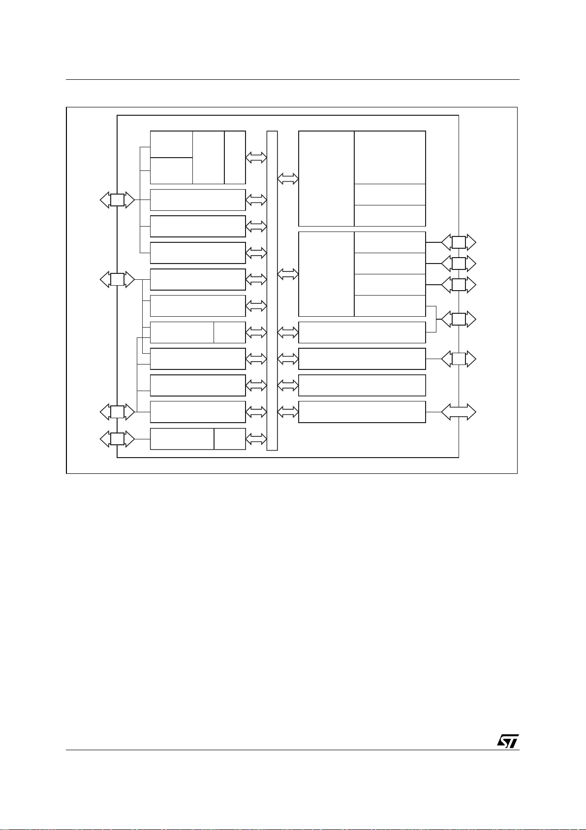
Figure 2. Block Diagram
(3) 16-bit
Timer/
Counters
(2)
External
Interrupts
P3.0:7
P1.0:7
Optional IrDA
Encoder/Decoder
Turbo
8032
Core
I2C
UART0
(8) GPIO, Port 3
(8) GPIO, Port 1
(8) 10-bit ADC
PFQ
&
BC
UART1
uPSD34xx
Programmable
Programmable
SYSTEM BUS
Decode and
Page Logic
General
Purpose
Logic,
16 Macrocells
JTAG ICE and ISP
1st Flash Memory:
64K, 128K, or
256K Bytes
2nd Flash Memory:
32K Bytes
SRAM:
4K or 8K Bytes
(8) GPIO, Port A
(80-pin only)
(8) GPIO, Port B
(2) GPIO, Port D
(4) GPIO, Port C
PA0:7
PB0:7
PD1:2
PC0:7
P4.0:7
USB+,
USB–
SPI
16-bit PCA
(6) PWM, CAPCOM, TIMER
(8) GPIO, Port 4
USB v2.0,
Full Speed
10
FIFOs
8032 Address/Data/Control Bus
(80-pin device only)
Supervisor:
Watchdog and Low-Voltage Reset
VCC, VDD, GND, Reset, Crystal In
MCU
Bus
Dedicated
Pins
AI09695
8/264
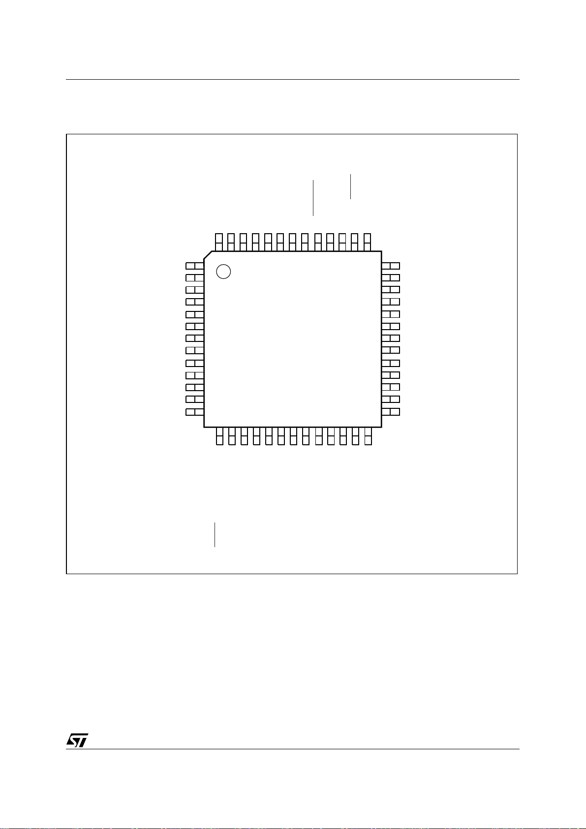
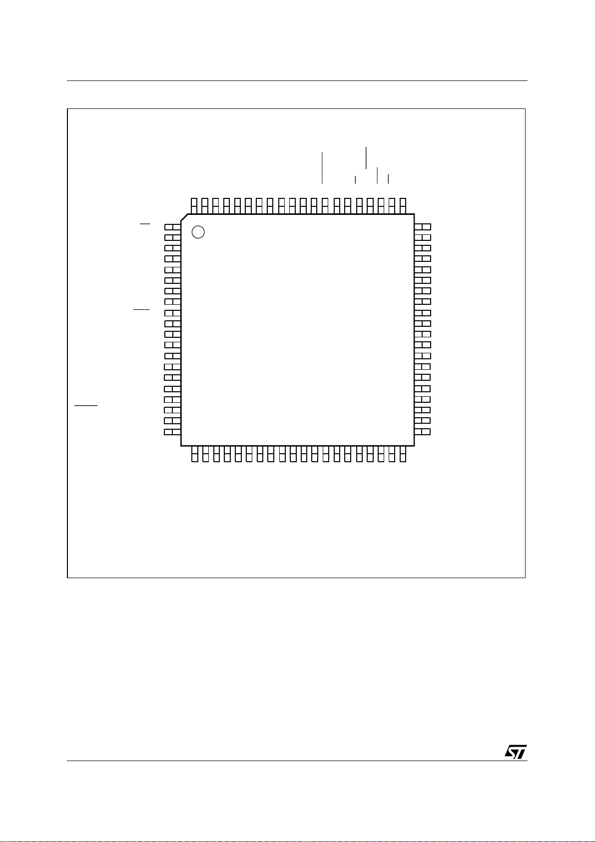
PIN DESCRIPTIONS
Figure 3. TQFP52 Connections
uPSD34xx - PIN DESCRIPTIONS
/ADC7
(2)
PB6
(2)
PB7
P1.7/SPISEL
(3)
REF
/V
CC
PB5
GND
PB0
PB1
PB2
PB3
PB4
AV
RESET_IN
52515049484746454443424140
/ADC6
P1.6/SPITXD
PD1/CLKIN
PC7
JTAG TDO
JTAG TDI
DEBUG
3.3V V
CC
USB+
V
DD
GND
USB–
PC2/V
STBY
JTAG TCK
JTAG TMS
(2)
(2)
(2)
(2)
/ADC1
/ADC0
/ADC5
/ADC4
(2)
/ADC3
(2)
/ADC2
1
2
3
4
5
6
7
(1)
8
9
10
11
12
13
39 P1.5/SPIRXD
38 P1.4/SPICLK
37 P1.3/TXD1(IrDA)
36 P1.2/RXD1(IrDA)
35 P1.1/T2X
34 P1.0/T2
(1)
33 V
DD
32 XTAL2
31 XTAL1
30 P3.7/SCL
29 P3.6/SDA
28 P3.5/C1
27 P3.4/C0
14151617181920212223242526
GND
TXD0/P3.1
/TCM4/P4.5
/TCM5/P4.6
/TCM3/P4.4
(2)
(2)
SPITXD
SPIRXD
(2)
SPICLK
/PCACLK1/P4.7
(2)
SPISEL
/TCM2/P4.2
(2)
/PCACLK0/P4.3
(2)
RXD1(IrDA)
TXD1(IrDA)
RXD0/P3.0
/TCM1/P4.1
/TCM0/P4.0
(2)
(2)
T2
T2X
EXTINT0/TG0/P3.2
EXTINT1/TG1/P3.3
AI09696
Note: 1. For 5V applications, VDD must be connected to a 5.0V source. For 3.3V applications, VDD must be connected to a 3.3V source.
2. These signals can be used on one of two different ports (Port 1 or Port 4) for flexibility. Default is Port1.
3. AV
and 3.3V AVCC are shared in the 52-pin package only. ADC channels must use 3.3V as AV
REF
for the 52-pin package.
REF
9/264
uPSD34xx - PIN DESCRIPTIONS
Figure 4. TQFP80 Connections
SPISEL
SPITXD
PD2/CSI
P3.3/TG1/EXINT1
PD1/CLKIN
ALE
PC7
JTAG TDO
JTAG TDI
DEBUG
PC4/TERR
3.3V V
USB+
V
DD
GND
USB–
PC3/TSTAT
PC2/V
STBY
JTAG TCK
(2)
/PCACLK1/P4.7
(2)
/TCM5/P4.6
JTAG TMS
/ADC7
(3)
CC
PB0
P3.2/EXINT0/TG0
PB1
P3.1/TXD0
PB2
P3.0/RXD0
PB3
PB4
AV
PB5
V
REF
GND
RESET_IN
PB6
PB7RDP1.7/SPISEL
80797877767574737271706968676665646362
1
2
3
4
5
6
7
8
9
10
CC
(1)
11
(2)
12
13
14
15
16
17
18
19
20
/ADC6
(3)
PSENWRP1.6/SPITXD
61
60 P1.5/SPIRXD
59 P1.4/SPICLK
58 P1.3/TXD1(IrDA)
57 NC
56 P1.2/RXD1(IrDA)
55 NC
54 P1.1/T2X
53 NC
52 P1.0/T2
51 NC
50 V
49 XTAL2
48 XTAL1
47 MCU AD7
46 P3.7/SCL
45 MCU AD6
44 P3.6/SDA
43 MCU AD5
42 P3.5/C1
41 MCU AD4
(3)
/ADC5
(3)
/ADC4
(3)
/ADC3
(3)
/ADC2
(3)
/ADC1
(3)
/ADC0
(1)
DD
21222324252627282930313233343536373839
PA7
PA6
/TCM4/P4.5
(2)
SPIRXD
PA5
/TCM3/P4.4
(2)
SPICLK
PA3
PA4
/PCACLK0/P4.3
(2)
GND
PA2
/TCM1/P4.1
/TCM2/P4.2
(2)
(2)
T2X
PA1
PA0
/TCM0/P4.0
(2)
T2
MCU AD0
MCU AD1
MCU AD2
RXD1(IrDA)
TXD1(IrDA)
Note: NC = Not Connected
Note: 1. The USB+ pin needs a 1.5kΩ pull-up resistor.
2. For 5V applications, V
3. These signals can be used on one of two different ports (Port 1 or Port 4) for flexibility. Default is Port1.
must be connected to a 5.0V source. For 3.3V applications, VDD must be connected to a 3.3V source.
DD
10/264
40
P3.4/C0
MCU AD3
AI09697

uPSD34xx - PIN DESCRIPTIONS
Table 2. Pin Definitions
Function
Timer 2 Count input
(T2)
Timer 2 Trigger input
(T2X)
UART1 or IrDA
Receive (RxD1)
UART or IrDA
Transmit (TxD1)
SPI Clock Out
(SPICLK)
SPI Receive
(SPIRxD)
SPI Transmit
(SPITxD)
SPI Slave Select
(SPISEL)
UART0 Receive
(RxD0)
UART0 Transmit
(TxD0)
Interrupt 0 input
(EXTINT0)/Timer 0
gate control (TG0)
Interrupt 1 input
(EXTINT1)/Timer 1
gate control (TG1)
2
C Bus serial data
I
2
CSDA)
(I
2
I
C Bus clock
2
CSCL)
(I
Program Counter
Array0 PCA0-TCM0
Port Pin
Signal
Name
80-Pin
No.
52-Pin
(1)
No.
In/Out
Basic Alternate 1 Alternate 2
External Bus
MCUAD0 AD0 36 N/A I/O
Multiplexed Address/
Data bus A0/D0
MCUAD1 AD1 37 N/A I/O
MCUAD2 AD2 38 N/A I/O
MCUAD3 AD3 39 N/A I/O
MCUAD4 AD4 41 N/A I/O
MCUAD5 AD5 43 N/A I/O
MCUAD6 AD6 45 N/A I/O
MCUAD7 AD7 47 N/A I/O
P1.0
P1.1
P1.2
P1.3
P1.4
P1.5
P1.6
P1.7
T2
ADC0
T2X
ADC1
RxD1
ADC2
TXD1
ADC3
SPICLK
ADC4
SPIRxD
ADC6
SPITXD
ADC6
SPISEL
ADC7
52 34 I/O General I/O port pin
54 35 I/O General I/O port pin
56 36 I/O General I/O port pin
58 37 I/O General I/O port pin
59 38 I/O General I/O port pin
60 39 I/O General I/O port pin
61 40 I/O General I/O port pin
64 41 I/O General I/O port pin
Multiplexed Address/
Data bus A1/D1
Multiplexed Address/
Data bus A2/D2
Multiplexed Address/
Data bus A3/D3
Multiplexed Address/
Data bus A4/D4
Multiplexed Address/
Data bus A5/D5
Multiplexed Address/
Data bus A6/D6
Multiplexed Address/
Data bus A7/D7
P3.0 RxD0 75 23 I/O General I/O port pin
P3.1 TXD0 77 24 I/O General I/O port pin
P3.2
EXINT0
TGO
79 25 I/O General I/O port pin
P3.3 INT1 2 26 I/O General I/O port pin
P3.4 C0 40 27 I/O General I/O port pin Counter 0 input (C0)
P3.5 C1 42 28 I/O General I/O port pin Counter 1 input (C1)
P3.6 SDA 44 29 I/O General I/O port pin
P3.7 SCL 46 30 I/O General I/O port pin
P4.0
T2
TCM0
33 22 I/O General I/O port pin
ADC Channel 0
input (ADC0)
ADC Channel 1
input (ADC1)
ADC Channel 2
input (ADC2)
ADC Channel 3
input (ADC3)
ADC Channel 4
input (ADC4)
ADC Channel 5
input (ADC5)
ADC Channel 6
input (ADC6)
ADC Channel 7
input (ADC7)
Timer 2 Count input
(T2)
11/264
uPSD34xx - PIN DESCRIPTIONS
Port Pin
P4.1
P4.2
P4.3
P4.4
P4.5
Signal
Name
T2X
TCM1
RXD1
TCM2
TXD1
PCACLK0
SPICLK
TCM3
SPIRXD
TCM4
80-Pin
No.
52-Pin
No.
(1)
In/Out
Basic Alternate 1 Alternate 2
31 21 I/O General I/O port pin PCA0-TCM1
30 20 I/O General I/O port pin PCA0-TCM2
27 18 I/O General I/O port pin PCACLK0
25 17 I/O General I/O port pin
Program Counter
Array1 PCA1-TCM3
23 16 I/O General I/O port pin PCA1-TCM4
P4.6 SPITXD 19 15 I/O General I/O port pin PCA1-TCM5
P4.7
V
REF
RD
WR
PSEN
ALE 4 N/A O
RESET_IN
XTAL1 48 31 I
XTAL2 49 32 O
DEBUG 8 5 I/O
SPISEL
PCACLK1
18 14 I/O General I/O port pin PCACLK1
70 N/A I
65 N/A O
62 N/A O
63 N/A O
Reference Voltage
input for ADC
READ Signal,
external bus
WRITE Signal,
external bus
PSEN Signal,
external bus
Address Latch
signal, external bus
68 44 I
Active low reset
input
Oscillator input pin
for system clock
Oscillator output pin
for system clock
I/O to the MCU
Debug Unit
PA0 35 N/A I/O General I/O port pin
PA1 34 N/A I/O General I/O port pin
PA2 32 N/A I/O General I/O port pin
PA3 28 N/A I/O General I/O port pin
PA4 26 N/A I/O General I/O port pin
PA5 24 N/A I/O General I/O port pin
PA6 22 N/A I/O General I/O port pin
PA7 21 N/A I/O General I/O port pin
PB0 80 52 I/O General I/O port pin
PB1 78 51 I/O General I/O port pin
PB2 76 50 I/O General I/O port pin
PB3 74 49 I/O General I/O port pin
PB4 73 48 I/O General I/O port pin
PB5 71 46 I/O General I/O port pin
PB6 67 43 I/O General I/O port pin
PB7 66 42 I/O General I/O port pin
JTAGTMS TMS 20 13 I JTAG pin (TMS)
JTAGTCK TCK 17 12 I JTAG pin (TCK)
Function
Timer 2 Trigger input
(T2X)
UART1 or IrDA
Receive (RxD1)
UART1 or IrDA
Transmit (TxD1)
SPI Clock Out
(SPICLK)
SPI Receive
(SPIRxD)
SPI Transmit
(SPITxD)
SPI Slave Select
(SPISEL)
All Port A pins
support:
1. PLD Macro-cell
outputs, or
2. PLD inputs, or
3. Latched
Address Out
(A0-A7), or
4. Peripheral I/O
Mode
All Port B pins
support:
1. PLD Macro-cell
outputs, or
2. PLD inputs, or
3. Latched
Address Out
(A0-A7)
12/264
uPSD34xx - PIN DESCRIPTIONS
Port Pin
PC2
Signal
Name
V
STBY
80-Pin
No.
52-Pin
No.
(1)
In/Out
Basic Alternate 1 Alternate 2
16 11 I/O General I/O port pin
PC3 TSTAT 15 N/A I/O General I/O port pin
PC4 TERR
9 N/A I/O General I/O port pin
JTAGTDI TDI 7 4 I JTAG pin (TDI)
JTAGTDO TDO 6 3 O JTAG pin (TDO)
PC7 5 2 I/O General I/O port pin
PD1 CLKIN 3 1 I/O General I/O port pin
PD2 CSI 1 N/A I/O General I/O port pin
USB D+ pin; 1.5kΩ
USB+ 11 7 I/O
pull-up resistor is
required.
USB– 14 10 I/O USB D– pin
3.3V-V
CC
AV
CC
V
DD
3.3V or 5V
V
DD
3.3V or 5V
10 6
72 47
12 8
50 33
V
- MCU Module
CC
Analog V
V
- PSD Module
DD
- 3.3V for 3V
V
DD
- 5V for 5V
V
DD
V
- PSD Module
DD
- 3.3V for 3V
V
DD
- 5V for 5V
V
DD
CC
GND 13 9
GND 29 19
GND 69 45
NC 11 N/A
NC
NC
NC
NC
Note: 1. N/A = Signal Not Available on 52-pin package.
51
53
55
57
N/A
N/A
N/A
N/A
Input
Function
SRAM Standby
voltage input
(V
)
STBY
Optional JTAG
Status (TSTAT)
Optional JTAG
Status (TERR
PLD Macrocell
output, or PLD input
PLD, Macrocell
output, or PLD input
PLD, Macrocell
)
output, or PLD input
PLD, Macrocell
output, or PLD input
1. PLD I/O
2. Clock input to
PLD and APD
1. PLD I/O
2. Chip select ot
PSD Module
13/264

uPSD34xx - HARDWARE DESCRIPTION
HARDWARE DESCRIPTION
The uPSD34xx has a modular architecture built
from a stacked die process. There are two die, one
is designated “MCU Module” in this document, and
the other is designated “PSD Module” (see Figure
5., page 15). In all cases, the MCU Module die op-
erates at 3.3V with 5V tolerant I/O. The PSD Module is either a 3.3V die or a 5V die, depending on
the uPSD34xx device as described below.
The MCU Module consists of a fast 8032 core, that
operates with 4 clocks per instruction cycle, and
has many peripheral and system supervisor functions. The PSD Module provides the 8032 with
multiple memories (two Flash and one SRAM) for
program and data, programmable logic for address decoding and for general-purpose logic, and
additional I/O. The MCU Module communicates
with the PSD Module through internal address and
data busses (AD0 – AD15) and control signals
, WR, PSEN, ALE, RESET).
(RD
There are slightly different I/O characteristics for
each module. I/Os for the MCU module are designated as Ports 1, 3, and 4. I/Os for the PSD Module are designated as Ports A, B, C, and D.
For all 5V uPSD34xx devices, a 3.3V MCU Module
is stacked with a 5V PSD Module. In this case, a
5V uPSD34xx device must be supplied with
3.3V
PSD Module. Ports 3 and 4 of the MCU Module
are 3.3V ports with tolerance to 5V devices (they
can be directly driven by external 5V devices and
they can directly drive external 5V devices while
for the MCU Module and 5.0VDD for the
CC
producing a V
of 2.4V min and VCC max). Ports
OH
A, B, C, and D of the PSD Module are true 5V
ports.
For all 3.3V uPSD34xxV devices, a 3.3V MCU
Module is stacked with a 3.3V PSD Module. In this
case, a 3.3V uPSD34xx device needs to be supplied with a single 3.3V voltage source at both V
CC
and VDD. I/O pins on Ports 3 and 4 are 5V tolerant
and can be connected to external 5V peripherals
devices if desired. Ports A, B, C, and D of the PSD
Module are 3.3V ports, which are not tolerant to
external 5V devices.
Refer to Table 3 for port type and voltage source
requirements.
80-pin uPSD34xx devices provide access to 8032
address, data, and control signals on external pins
to connect external peripheral and memory devices. 52-pin uPSD34xx devices do not provide access to the 8032 system bus.
All non-volatile memory and configuration portions
of the uPSD34xx device are programmed through
the JTAG interface and no special programming
voltage is needed. This same JTAG port is also
used for debugging of the 8032 core at runtime
providing breakpoint, single-step, display, and
trace features. A non-volatile security bit may be
programmed to block all access via JTAG interface for security. The security bit is defeated only
by erasing the entire device, leaving the device
blank and ready to use again.
Table 3. Port Type and Voltage Source Combinations
V
Device Type
5V:
uPSD34xx
3.3V:
uPSD34xxV
14/264
for MCU
CC
Module
3.3V 5.0V
3.3V 3.3V
VDD for PSD
Module
Ports 1, 3, and 4 on MCU
3.3V (Ports 3 and 4 are
3.3V (Ports 3 and 4 are
Module
5V tolerant)
5V tolerant)
Ports A, B, C, and D on
PSD Module
5V
3.3V. NOT 5V tolerant
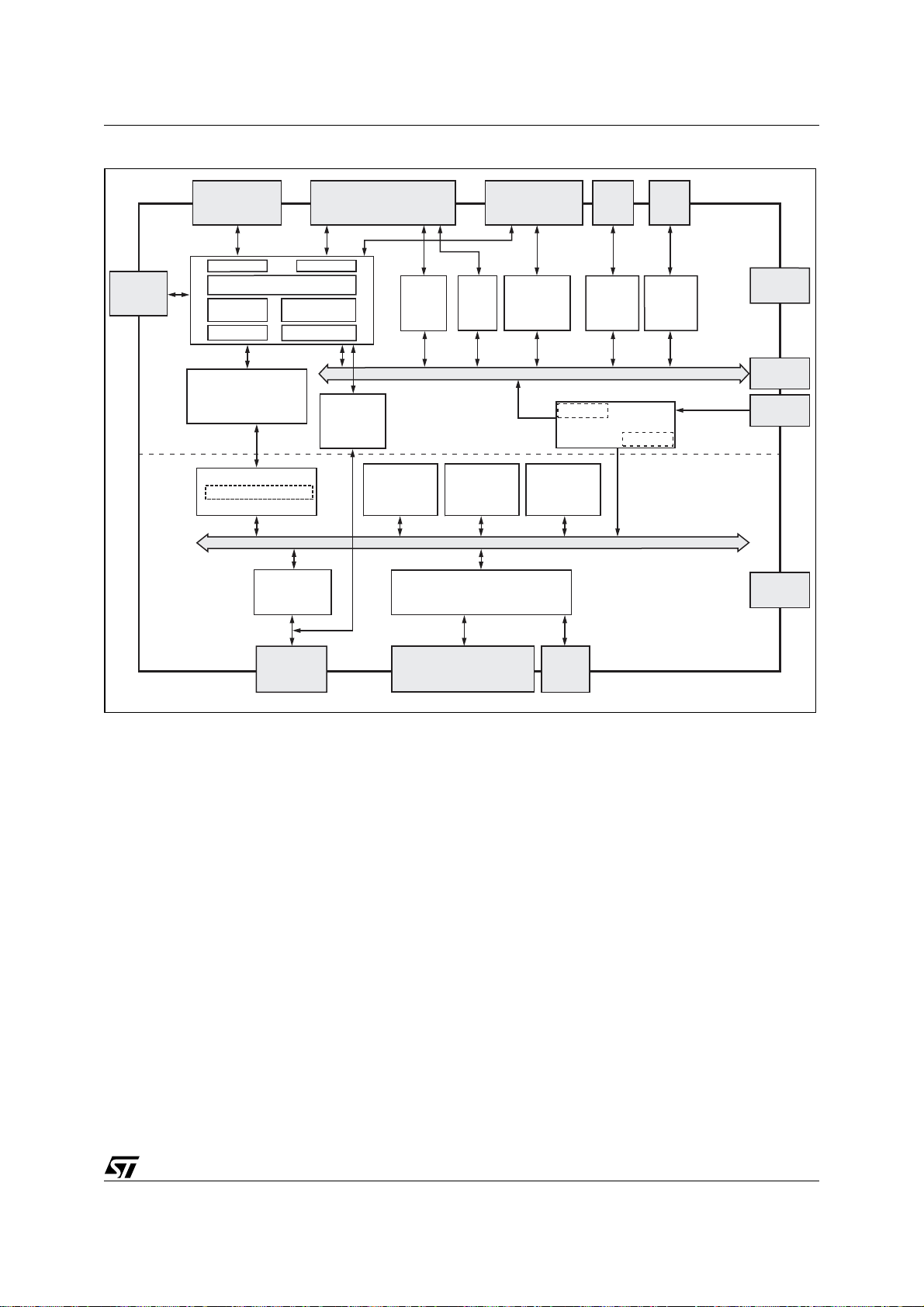
Figure 5. Functional Modules
uPSD34xx - HARDWARE DESCRIPTION
XTAL
Clock Unit
Die-to-Die Bus
8-Bit/16-Bit
Port 3 - UART0,
Intr, Timers
Turbo 8032 Core
Dual
UARTs
Inte rrupt
256 Byte SRAM
Dedicated Memory
Interface Prefetch,
Branch Cache
Enha nce d MCU Interface
PSD Page Register
Dec ode P LD
JTAG ISP
Port 1 - Timer, ADC, SPI
Port 1Port 3
3 Timer /
Counters
JTAG
DEBUG
Main Flash
10-bit
ADC
8032 Internal Bus
SPI
Secondary
Flash
PSD Interna l Bus
CPLD - 16 MACROCELLS
Port 4 - PCA,
PWM, UART1
PCA
PWM
Counters
Internal
Reset
SRAM
LVD
Reset Logic
Port 3
2
I
C
I2C
Unit
WDT
PSD
Reset
USB
pins
USB and
Trans-
ceiver
MCU Module
Reset Input
PSD Module
VCC Pins
3.3V
Ext.
Bus
Reset
Pin
VDD Pins
3.3V or 5V
uPSD34xx
Port C
JTAG and
GPIO
Port A,B,C PLD
I/O and GPIO
Port D
GPIO
AI10409
15/264

uPSD34xx - MEMORY ORGANIZATION
MEMORY ORGANIZATION
The 8032 MCU core views memory on the MCU
module as “internal” memory and it views memory
on the PSD module as “external” memory, see
Figure 6.
Internal memory on the MCU Module consists of
DATA, IDATA, and SFRs. These standard 8032
memories reside in 384 bytes of SRAM located at
a fixed address space starting at address 0x0000.
External memory on the PSD Module consists of
four types: main Flash (64K, 128K, or 256K bytes),
a smaller secondary Flash (32K), SRAM (4K or 8K
bytes), and a block of PSD Module control registers called csiop (256 bytes). These external memories reside at programmable address ranges,
specified using the software tool PSDsoft Express.
See the PSD Module section of this document for
more details on these memories.
External memory is accessed by the 8032 in two
separate 64K byte address spaces. One address
space is for program memory and the other ad-
Figure 6. uPSD34xx Memories
dress space is for data memory. Program memory
is accessed using the 8032 signal, PSEN
. Data
memory is accessed using the 8032 signals, RD
and WR. If the 8032 needs to access more than
64K bytes of external program or data memory, it
must use paging (or banking) techniques provided
by the Page Register in the PSD Module.
Note: When referencing program and data memory spaces, it has nothing to do with 8032 internal
SRAM areas of DATA, IDATA, and SFR on the
MCU Module. Program and data memory spaces
only relate to the external memories on the PSD
Module.
External memory on the PSD Module can overlap
the internal SRAM memory on the MCU Module in
the same physical address range (starting at
0x0000) without interference because the 8032
core does not assert the RD
or WR signals when
accessing internal SRAM.
Fixed
Addresses
FF
80
7F
0
Internal SRAM on
MCU Module
384 Bytes SRAM
Indirect
Addressing
I DATA
128 Bytes
128 Bytes
DATA
Direct or Indirect Addressing
SFR
128 Bytes
Direct
Addressing
Main
Flash
64KB
or
128KB
or
256KB
External Memory on
PSD Module
• External memories may be placed at virtually
any address using software tool PSDsoft Express.
• The SRAM and Flash memories may be placed
in 8032 Program Space or Data Space using
PSDsoft Express.
• Any memory in 8032 Data Space is XDATA.
Secondary
Flash
32KB
SRAM
4KB
or
8KB
AI10410
16/264

uPSD34xx - MEMORY ORGANIZATION
Internal Memory (MCU Module, Standard 8032
Memory: DATA, IDATA, SFR)
DATA Memory. The first 128 bytes of internal
SRAM ranging from address 0x0000 to 0x007F
are called DATA, which can be accessed using
8032 direct or indirect addressing schemes and
are typically used to store variables and stack.
Four register banks, each with 8 registers (R0 –
R7), occupy addresses 0x0000 to 0x001F. Only
one of these four banks may be enabled at a time.
The next 16 locations at 0x0020 to 0x002F contain
128 directly addressable bit locations that can be
used as software flags. SRAM locations 0x0030
and above may be used for variables and stack.
IDATA Memory. The next 128 bytes of internal
SRAM are named IDATA and range from address
0x0080 to 0x00FF. IDATA can be accessed only
through 8032 indirect addressing and is typically
used to hold the MCU stack as well as data variables. The stack can reside in both DATA and
IDATA memories and reach a size limited only by
the available space in the combined 256 bytes of
these two memories (since stack accesses are always done using indirect addressing, the boundary between DATA and IDATA does not exist with
regard to the stack).
SFR Memory. Special Function Registers (Table
5., page 25) occupy a separate physical memory,
but they logically overlap the same 128 bytes as
IDATA, ranging from address 0x0080 to 0x00FF.
SFRs are accessed only using direct addressing.
There 86 active registers used for many functions:
changing the operating mode of the 8032 MCU
core, controlling 8032 peripherals, controlling I/O,
and managing interrupt functions. The remaining
unused SFRs are reserved and should not be accessed.
16 of the SFRs are both byte- and bit-addressable.
Bit-addressable SFRs are those whose address
ends in “0” or “8” hex.
External Memory (PSD Module: Program
memory, Data memory)
The PSD Module has four memories: main Flash,
secondary Flash, SRAM, and csiop. See the PSD
MODULE section for more detailed information on
these memories.
Memory mapping in the PSD Module is implemented with the Decode PLD (DPLD) and optionally the Page Register. The user specifies decode
equations for individual segments of each of the
memories using the software tool PSDsoft Express. This is a very easy point-and-click process
allowing total flexibility in mapping memories. Additionally, each of the memories may be placed in
various combinations of 8032 program address
space or 8032 data address space by using the
software tool PSDsoft Express.
Program Memory. External program memory is
addressed by the 8032 using its 16-bit Program
Counter (PC) and is accessed with the 8032 signal, PSEN
any address in program space between 0x0000
and 0xFFFF.
After a power-up or reset, the 8032 begins program execution from location 0x0000 where the
reset vector is stored, causing a jump to an initialization routine in firmware. At address 0x0003, just
following the reset vector are the interrupt service
locations. Each interrupt is assigned a fixed interrupt service location in program memory. An interrupt causes the 8032 to jump to that service
location, where it commences execution of the
service routine. External Interrupt 0 (EXINT0), for
example, is assigned to service location 0x0003. If
EXINT0 is going to be used, its service routine
must begin at location 0x0003. Interrupt service locations are spaced at 8-byte intervals: 0x0003 for
EXINT0, 0x000B for Timer 0, 0x0013 for EXINT1,
and so forth. If an interrupt service routine is short
enough, it can reside entirely within the 8-byte interval. Longer service routines can use a jump instruction to somewhere else in program memory.
Data Memory. External data is referred to as
XDATA and is addressed by the 8032 using Indirect Addressing via its 16-bit Data Pointer Register
(DPTR) and is accessed by the 8032 signals, RD
and WR. XDATA can be present at any address in
data space between 0x0000 and 0xFFFF.
Note: the uPSD34xx has dual data pointers
(source and destination) making XDATA transfers
much more efficient.
Memory Placement. PSD Module architecture
allows the placement of its external memories into
different combinations of program memory and
data memory spaces. This means the main Flash,
the secondary Flash, and the SRAM can be
viewed by the 8032 MCU in various combinations
of program memory or data memory as defined by
PSDsoft Express.
As an example of this flexibility, for applications
that require a great deal of Flash memory in data
space (large lookup tables or extended data recording), the larger main Flash memory can be
placed in data space and the smaller secondary
Flash memory can be placed in program space.
The opposite can be realized for a different application if more Flash memory is needed for code
and less Flash memory for data.
. Program memory can be present at
17/264

uPSD34xx - 8032 MCU CORE PERFORMANCE ENHANCEMENTS
By default, the SRAM and csiop memories on the
PSD Module must always reside in data memory
space and they are treated by the 8032 as XDATA.
The main Flash and secondary Flash memories
may reside in program space, data space, or both.
These memory placement choices specified by
PSDsoft Express are programmed into non-volatile sections of the uPSD34xx, and are active at
power-up and after reset. It is possible to override
these initial settings during runtime for In-Application Programming (IAP).
Standard 8032 MCU architecture cannot write to
its own program memory space to prevent accidental corruption of firmware. However, this becomes an obstacle in typical 8032 systems when
a remote update to firmware in Flash memory is
required using IAP. The PSD module provides a
solution for remote updates by allowing 8032 firmware to temporarily “reclassify” Flash memory to
reside in data space during a remote update, then
returning Flash memory back to program space
when finished. See the VM Register (Table
104., page 174) in the PSD Module section of this
document for more details.
8032 MCU CORE PERFORMANCE ENHANCEMENTS
Before describing performance features of the
uPSD34xx, let us first look at standard 8032 architecture. The clock source for the 8032 MCU creates a basic unit of timing called a machine-cycle,
which is a period of 12 clocks for standard 8032
MCUs. The instruction set for traditional 8032
MCUs consists of 1, 2, and 3 byte instructions that
execute in different combinations of 1, 2, or 4 machine-cycles. For example, there are one-byte instructions that execute in one machine-cycle (12
clocks), one-byte instructions that execute in four
machine-cycles (48 clocks), two-byte, two-cycle
instructions (24 clocks), and so on. In addition,
standard 8032 architecture will fetch two bytes
from program memory on almost every machinecycle, regardless if it needs them or not (dummy
fetch). This means for one-byte, one-cycle instructions, the second byte is ignored. These one-byte,
one-cycle instructions account for half of the
8032's instructions (126 out of 255 opcodes).
There are inefficiencies due to wasted bus cycles
and idle bus times that can be eliminated.
The uPSD34xx 8032 MCU core offers increased
performance in a number of ways, while keeping
the exact same instruction set as the standard
8032 (all opcodes, the number of bytes per in-
struction, and the native number a machine-cycles
per instruction are identical to the original 8032).
The first way performance is boosted is by reducing the machine-cycle period to just 4 MCU clocks
as compared to 12 MCU clocks in a standard
8032. This shortened machine-cycle improves the
instruction rate for one- or two-byte, one-cycle instructions by a factor of three (Figure 7., page 19)
compared to standard 8051 architectures, and significantly improves performance of multiple-cycle
instruction types.
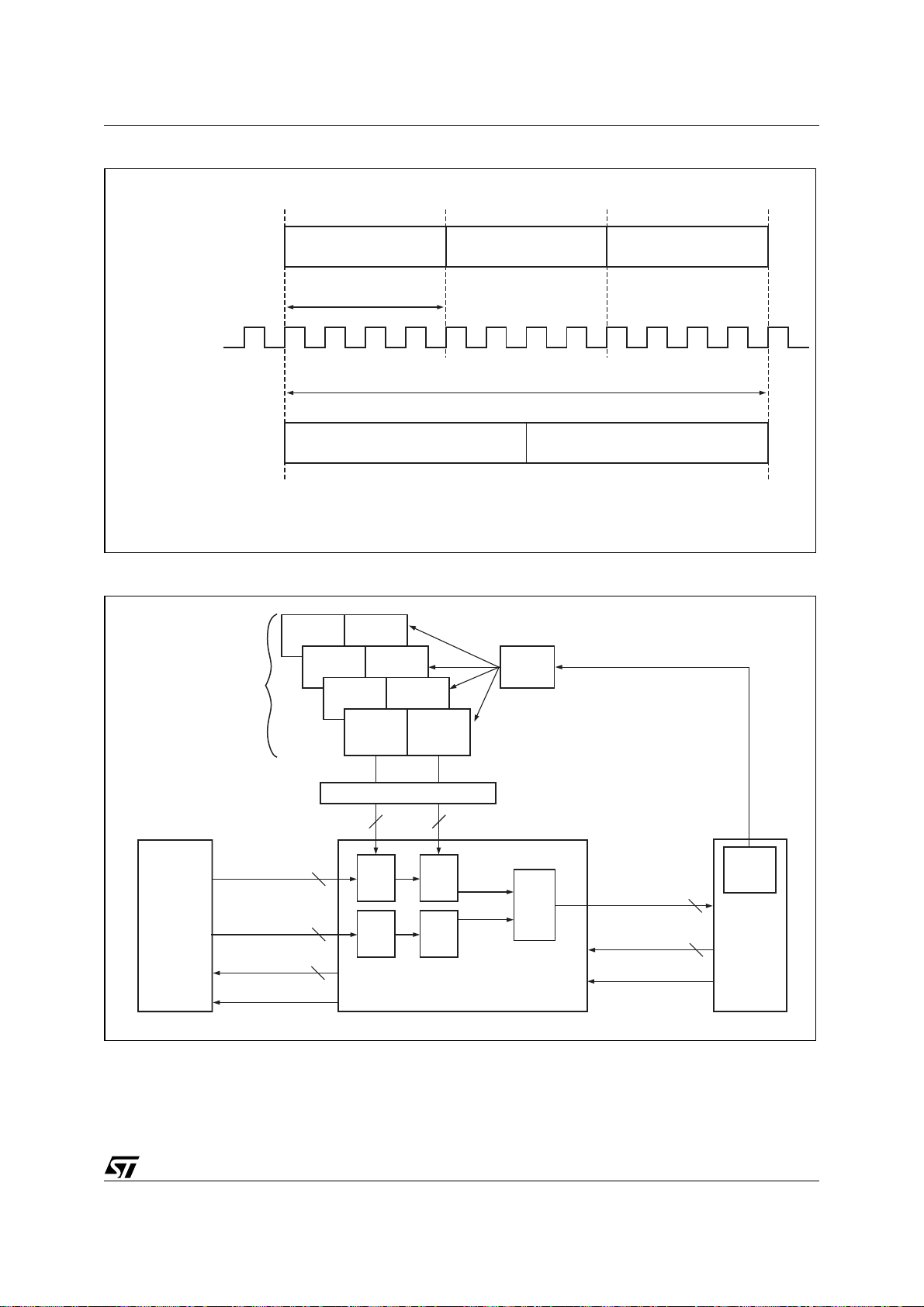
The example in Figure 7 shows a continuous execution stream of one- or two-byte, one-cycle instructions. The 5V uPSD34xx will yield 10 MIPS
peak performance in this case while operating at
40MHz clock rate. In a typical application however,
the effective performance will be lower since programs do not use only one-cycle instructions, but
special techniques are implemented in the
uPSD34xx to keep the effective MIPS rate as
close as possible to the peak MIPS rate at all
times. This is accomplished with an instruction
Pre-Fetch Queue (PFQ), a Branch Cache (BC),
and a 16-bit program memory bus as shown in
Figure 8., page 19.
18/264
uPSD34xx - 8032 MCU CORE PERFORMANCE ENHANCEMENTS
Figure 7. Comparison of uPSD34xx with Standard 8032 Performance
1- or 2-byte, 1-cycle Instructions
Instruction A Instruction B Instruction C
Turbo uPSD34xx
Execute Instruction and
Pre-Fetch Next Instruction
Execute Instruction and
Pre-Fetch Next Instruction
Execute Instruction and
Pre-Fetch Next Instruction
4 clocks (one machine cycle)
one machine cycle one machine cycle
MCU Clock
12 clocks (one machine cycle)
Instruction A
Standard 8032
Fetch Byte for Instruction A
Dummy Byte is Ignored (wasted bus access)
Turbo uPSD34xx executes instructions A, B, and C in the same
amount of time that a standard 8032 executes only Instruction A.
Figure 8. Instruction Pre-Fetch Queue and Branch Cache
Branch 4
Code
Branch
Cache
(BC)
Branch 3
Code
Branch 2
Code
Branch 4
Code
Branch 3
Code
Branch 1
Code
Compare
Branch 2
Code
Branch 1
Code
Execute Instruction A
and Fetch a Second Dummy Byte
AI10411
16-bit
Program
Memory
on PSD
Module
Instruction Byte
Instruction Byte
Address
Wait
Load on Branch Address Match
1616
8
8
4 Bytes of Instruction
16
Instruction Pre-Fetch Queue (PFQ)
Instruction Byte
Address
Wait
Current
Branch
Address
8
8032
MCU
16
AI10431
19/264

uPSD34xx - 8032 MCU CORE PERFORMANCE ENHANCEMENTS
Pre-Fetch Queue (PFQ) and Branch Cache
(BC)
The PFQ is always working to minimize the idle
bus time inherent to 8032 MCU architecture, to
eliminate wasted memory fetches, and to maximize memory bandwidth to the MCU. The PFQ
does this by running asynchronously in relation to
the MCU, looking ahead to pre-fetch two bytes
(word) of code from program memory during any
idle bus periods. Only necessary word will be
fetched (no dummy fetches like standard 8032).
The PFQ will queue up to four code bytes in advance of execution, which significantly optimizes
sequential program performance. However, when
program execution becomes non-sequential (program branch), a typical pre-fetch queue will empty
itself and reload new code, causing the MCU to
stall. The Turbo uPSD34xx diminishes this problem by using a Branch Cache with the PFQ. The
BC is a four-way, fully associative cache, meaning
that when a program branch occurs, its branch
destination address is compared simultaneously
with four recent previous branch destinations
stored in the BC. Each of the four cache entries
contain up to four bytes of code related to a
branch. If there is a hit (a match), then all four code
bytes of the matching program branch are transferred immediately and simultaneously from the
BC to the PFQ, and execution on that branch continues with minimal delay. This greatly reduces the
chance that the MCU will stall from an empty PFQ,
and improves performance in embedded control
systems where it is quite common to branch and
loop in relatively small code localities.
By default, the PFQ and BC are enabled after
power-up or reset. The 8032 can disable the PFQ
and BC at runtime if desired by writing to a specific
SFR (BUSCON).
The memory in the PSD module operates with
variable wait states depending on the value specified in the SFR named BUSCON. For example, a
5V uPSD34xx device operating at a 40MHz crystal
frequency requires four memory wait states (equal
to four MCU clocks). In this example, once the
PFQ has one word of code, the wait states become transparent and a full 10 MIPS is achieved
when the program stream consists of sequential
one- or two-byte, one machine-cycle instructions
as shown in Figure 7., page 19 (transparent because a machine-cycle is four MCU clocks which
equals the memory pre-fetch wait time that is also
four MCU clocks). But it is also important to understand PFQ operation on multi-cycle instructions.
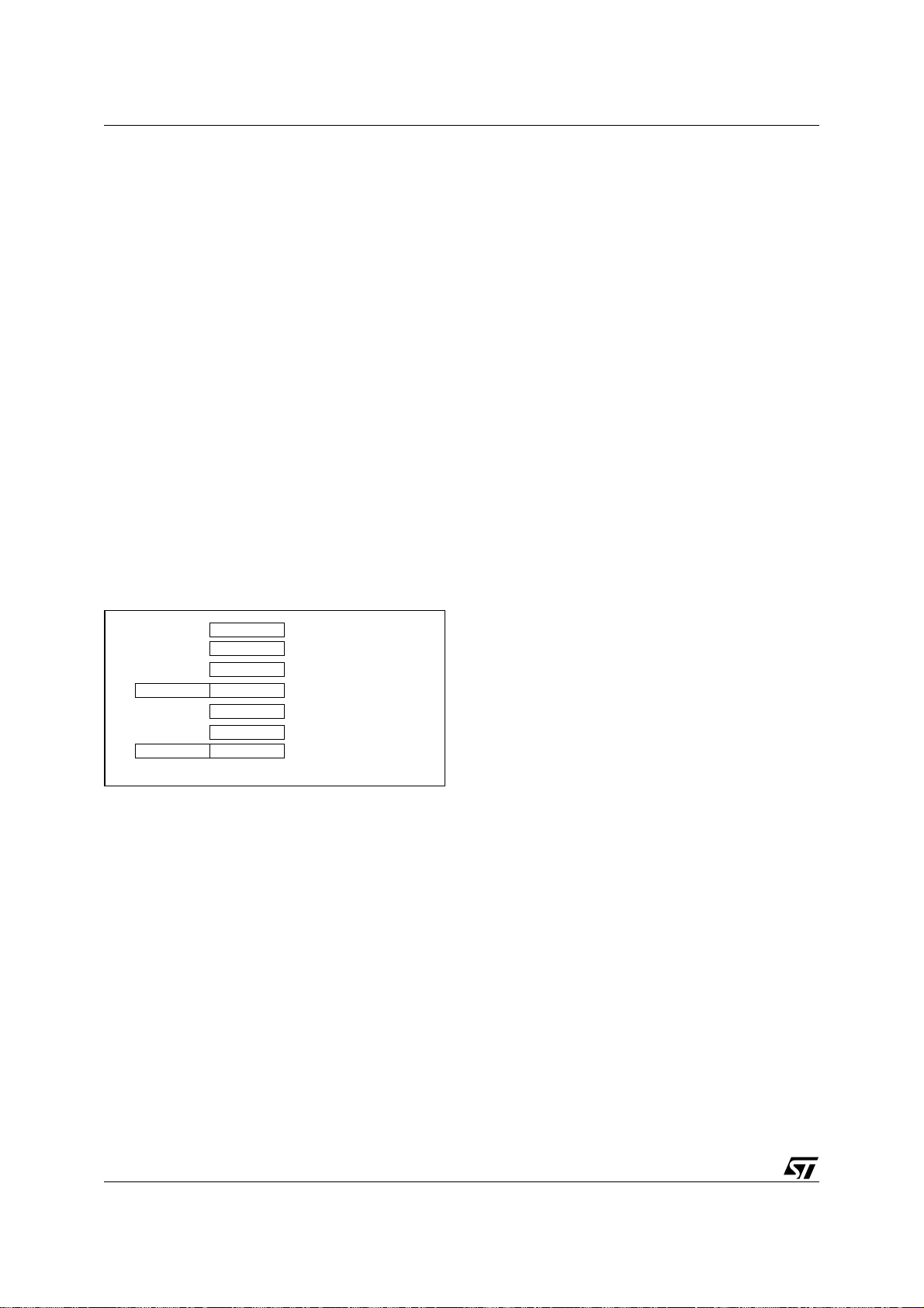
PFQ Example, Multi-cycle Instructions
Let us look at a string of two-byte, two-cycle instructions in Figure 9., page 21. There are three
instructions executed sequentially in this example,
instructions A, B, and C. Each of the time divisions
in the figure is one machine-cycle of four clocks,
and there are six phases to reference in this discussion. Each instruction is pre-fetched into the
PFQ in advance of execution by the MCU. Prior to
Phase 1, the PFQ has pre-fetched the two instruction bytes (A1 and A2) of Instruction A. During
Phase one, both bytes are loaded into the MCU
execution unit. Also in Phase 1, the PFQ is prefetching Instruction B (bytes B1 and B2) from program memory. In Phase 2, the MCU is processing
Instruction A internally while the PFQ is pre-fetching Instruction C. In Phase 3, both bytes of instruction B are loaded into the MCU execution unit and
the PFQ begins to pre-fetch bytes for the next instruction. In Phase 4 Instruction B is processed.
The uPSD34xx MCU instructions are an exact 1/3
scale of all standard 8032 instructions with regard
to number of cycles per instruction. Figure
10., page 21 shows the equivalent instruction se-
quence from the example above on a standard
8032 for comparison.
Aggregate Performance
The stream of two-byte, two-cycle instructions in
Figure 9., page 21, running on a 40MHz, 5V,
uPSD34xx will yield 5 MIPs. And we saw the
stream of one- or two-byte, one-cycle instructions
in Figure 7., page 19, on the same MCU yield 10
MIPs. Effective performance will depend on a
number of things: the MCU clock frequency; the
mixture of instructions types (bytes and cycles) in
the application; the amount of time an empty PFQ
stalls the MCU (mix of instruction types and misses on Branch Cache); and the operating voltage.
A 5V uPSD34xx device operates with four memory
wait states, but a 3.3V device operates with five
memory wait states yielding 8 MIPS peak compared to 10 MIPs peak for 5V device. The same
number of wait states will apply to both program
fetches and to data READ/WRITEs unless otherwise specified in the SFR named BUSCON.
In general, a 3X aggregate performance increase
is expected over any standard 8032 application
running at the same clock frequency.
20/264
uPSD34xx - 8032 MCU CORE PERFORMANCE ENHANCEMENTS
Figure 9. PFQ Operation on Multi-cycle Instructions
Three 2-byte, 2-cycle Instructions on uPSD34xx
Pre-Fetch
Inst A
Pre-Fetch Inst B and C Pre-Fetch next Inst
PFQ
MCU
Execution
Inst A, Byte 1&2 Inst B, Byte 1&2 Inst C, Byte 1&2 Next Inst
4-clock
Macine Cycle
Phase 1 Phase 2 Phase 3 Phase 4 Phase 6Phase 5
Previous Instruction A1 A2 Process A B1 B2 Process B C1 C2
Instruction A Instruction B Instruction C
Continue to Pre-Fetch
Figure 10. uPSD34xx Multi-cycle Instructions Compared to Standard 8032
Three 2-byte, 2-cycle Instructions, uPSD34xx vs. Standard 8032
24 Clocks Total (4 clocks per cycle)
uPSD34xx
Std 8032
A1
Byte 1
A2
Inst A
Byte 2
B1
1 Cycle
Process Inst A
B2
1 Cycle
Inst B
C1
C2
Inst C
72 Clocks (12 clocks per cycle)
Byte 1
Byte 2
Process Inst B
Byte 1
Byte 2
Process C
Process Inst C
Next Inst
AI10432
AI10412
21/264
uPSD34xx - MCU MODULE DISCRIPTION
MCU MODULE DISCRIPTION
This section provides a detail description of the
MCU Module system functions and peripherals, including:
■ 8032 MCU Registers
■ Special Function Registers
■ 8032 Addressing Modes
■ uPSD34xx Instruction Set Summary
■ Dual Data Pointers
■ Debug Unit
■ Interrupt System
■ MCU Clock Generation
■ Power Saving Modes
■ Oscillator and External Components
■ I/O Ports
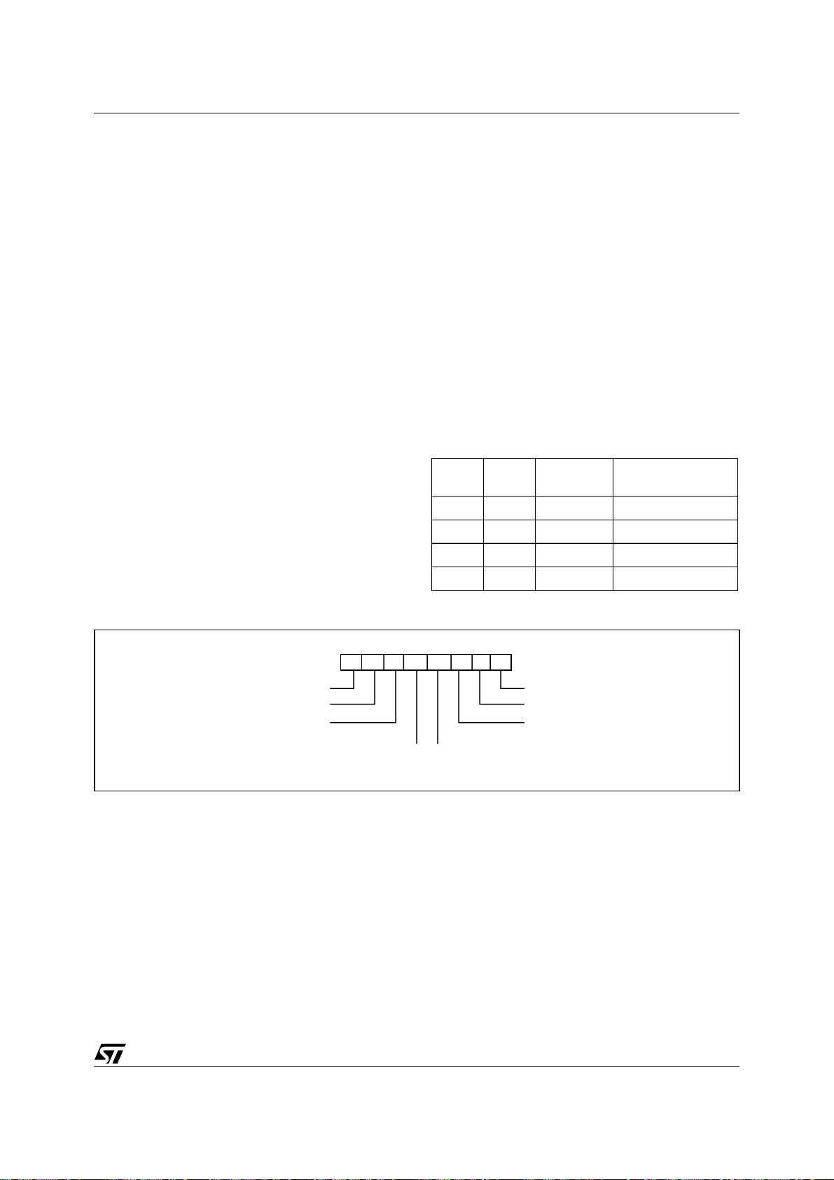
8032 MCU REGISTERS
The uPSD34xx has the following 8032 MCU core
registers, also shown in Figure 11.
Figure 11. 8032 MCU Registers
A
B
SP
PCH
DPTR(DPH)
AI06636
PCL
PSW
R0-R7
DPTR(DPL)
Stack Pointer (SP)
The SP is an 8-bit register which holds the current
location of the top of the stack. It is incremented
before a value is pushed onto the stack, and decremented after a value is popped off the stack. The
SP is initialized to 07h after reset. This causes the
stack to begin at location 08h (top of stack). To
avoid overlapping conflicts, the user must initialize
the top of the stack to 20h if all four banks of registers R0 - R7 are used, as well as the top of stack
to 30h if all of the 8032 bit memory locations are
used.
Data Pointer (DPTR)
DPTR is a 16-bit register consisting of two 8-bit
registers, DPL and DPH. The DPTR Register is
used as a base register to create an address for indirect jumps, table look-up operations, and for external data transfers (XDATA). When not used for
Accumulator
B Register
Stack Pointer
Program Counter
Program Status Word
General Purpose
Register (Bank0-3)
Data Pointer Register
■ MCU Bus Interface
■ Supervisory Functions
■ Standard 8032 Timer/Counters
■ Serial UART Interfaces
■ IrDA Interface
2
■ I
C Interface
■ SPI Interface
■ Analog to Digital Converter
■ Programmable Counter Array (PCA)
■ USB Interface
Note: A full description of the 8032 instruction set
may be found in the uPSD34xx Programmers
Guide.
addressing, the DPTR Register can be used as a
general purpose 16-bit data register.
Very frequently, the DPTR Register is used to access XDATA using the External Direct addressing
mode. The uPSD34xx has a special set of SFR
registers (DPTC, DPTM) to control a secondary
DPTR Register to speed memory-to-memory
XDATA transfers. Having dual DPTR Registers allows rapid switching between source and destination addresses (see details in DUAL DATA
POINTERS, page 38).
Program Counter (PC)
The PC is a 16-bit register consisting of two 8-bit
registers, PCL and PCH. This counter indicates
the address of the next instruction in program
memory to be fetched and executed. A reset forces the PC to location 0000h, which is where the reset jump vector is stored.
Accumulator (ACC)
This is an 8-bit general purpose register which
holds a source operand and receives the result of
arithmetic operations. The ACC Register can also
be the source or destination of logic and data
movement operations. For MUL and DIV instructions, ACC is combined with the B Register to hold
16-bit operands. The ACC is referred to as “A” in
the MCU instruction set.
B Register (B)
The B Register is a general purpose 8-bit register
for temporary data storage and also used as a 16bit register when concatenated with the ACC Register for use with MUL and DIV instructions.
22/264
General Purpose Registers (R0 - R7)
There are four banks of eight general purpose 8bit registers (R0 - R7), but only one bank of eight
registers is active at any given time depending on
the setting in the PSW word (described next). R0 R7 are generally used to assist in manipulating
values and moving data from one memory location
to another. These register banks physically reside
in the first 32 locations of 8032 internal DATA
SRAM, starting at address 00h. At reset, only the
first bank of eight registers is active (addresses
00h to 07h), and the stack begins at address 08h.
Program Status Word (PSW)
The PSW is an 8-bit register which stores several
important bits, or flags, that are set and cleared by
many 8032 instructions, reflecting the current
state of the MCU core. Figure 12., page 23 shows
the individual flags.
Carry Flag (CY). This flag is set when the last
arithmetic operation that was executed results in a
carry (addition) or borrow (subtraction). It is
cleared by all other arithmetic operations. The CY
flag is also affected by Shift and Rotate Instructions.
Auxiliary Carry Flag (AC). This flag is set when
the last arithmetic operation that was executed results in a carry into (addition) or borrow from (subtraction) the high-order nibble. It is cleared by all
other arithmetic operations.
uPSD34xx - 8032 MCU REGISTERS
General Purpose Flag (F0). This is a bit-addres-
sable, general-purpose flag for use under software
control.
Register Bank Select Flags (RS1, RS0). These
bits select which bank of eight registers is used
during R0 - R7 register accesses (see Table 4)
Overflow Flag (OV). The OV flag is set when: an
ADD, ADDC, or SUBB instruction causes a sign
change; a MUL instruction results in an overflow
(result greater than 255); a DIV instruction causes
a divide-by-zero condition. The OV flag is cleared
by the ADD, ADDC, SUBB, MUL, and DIV instructions in all other cases. The CLRV instruction will
clear the OV flag at any time.
Parity Flag (P). The P flag is set if the sum of the
eight bits in the Accumulator is odd, and P is
cleared if the sum is even.
Table 4. .Register Bank Select Addresses
RS1 RS0
0 0 0 00h - 07h
0 1 1 08h - 0Fh
1 0 2 10h - 17h
1 1 3 18h - 1Fh
Register
Bank
8032 Internal
DATA Address
Figure 12. Program Status Word (PSW) Register
MSB
CY
PSW
Carry Flag
Auxillary Carry Flag
General Purpose Flag
AC FO RS1 RS0 OV P
Register Bank Select Flags
(to select Bank0-3)
LSB
Reset Value 00h
Parity Flag
Bit not assigned
Overflow Flag
AI06639
23/264

uPSD34xx - SPECIAL FUNCTION REGISTERS (SFR)
SPECIAL FUNCTION REGISTERS (SFR)
A group of registers designated as Special Function Register (SFR) is shown in Table 5., page 25.
SFRs control the operating modes of the MCU
core and also control the peripheral interfaces and
I/O pins on the MCU Module. The SFRs can be accessed only by using the Direct Addressing method within the address range from 80h to FFh of
internal 8032 SRAM. Sixteen addresses in SFR
address space are both byte- and bit-addressable.
The bit-addressable SFRs are noted in Table 5.
106 of a possible 128 SFR addresses are occupied. The remaining unoccupied SFR addresses
(designated as “RESERVED” in Table 5) should
not be written. Reading unoccupied locations will
return an undefined value.
Note: There is a separate set of control registers
for the PSD Module, designated as csiop, and they
are described in the PSD MODULE, page 164.
The I/O pins, PLD, and other functions on the PSD
Module are NOT controlled by SFRs.
SFRs are categorized as follows:
■ MCU core registers:
IP, A, B, PSW, SP, DPTL, DPTH, DPTC,
DPTM
■ MCU Module I/O Port registers:
P1, P3, P4, P1SFS0, P1SFS1, P3SFS,
P4SFS0, P4SFS1
■ Standard 8032 Timer registers
TCON, TMOD, T2CON, TH0, TH1, TH2, TL0,
TL1, TL2, RCAP2L, RCAP2H
■ Standard Serial Interfaces (UART)
SCON0, SBUF0, SCON1, SBUF1
■ Power, clock, and bus timing registers
PCON, CCON0, CCON1, BUSCON
■ Hardware watchdog timer registers
WDKEY, WDRST
■ Interrupt system registers
IP, IPA, IE, IEA
■ Prog. Counter Array (PCA) control
registers
PCACL0, PCACH0, PCACON0, PCASTA,
PCACL1, PCACH1, PCACON1, CCON2,
CCON3
■ PCA capture/compare and PWM registers
CAPCOML0, CAPCOMH0, TCMMODE0,
CAPCOML1, CAPCOMH1, TCMMODE2,
CAPCOML2, CAPCOMH2, TCMMODE2,
CAPCOML3, CAPCOMH3, TCMMODE3,
CAPCOML4, CAPCOMH4, TCMMODE4,
CAPCOML5, CAPCOMH5, TCMMODE5,
PWMF0, PMWF1
■ SPI interface registers
SPICLKD, SPISTAT, SPITDR, SPIRDR,
SPICON0, SPICON1
2
■ I
C interface registers
S1SETUP, S1CON, S1STA, S1DAT, S1ADR
■ Analog to Digital Converter registers
ACON, ADCPS, ADAT0, ADAT1
■ IrDA interface register
IRDACON
■ USB interface registers
UADDR, UPAIR, WE0-3, UIF0-3, UCTL,
USTA, USEL, UCON, USIZE, UBASEH,
UBASEL, USCI, USCV
24/264
uPSD34xx - SPECIAL FUNCTION REGISTERS (SFR)
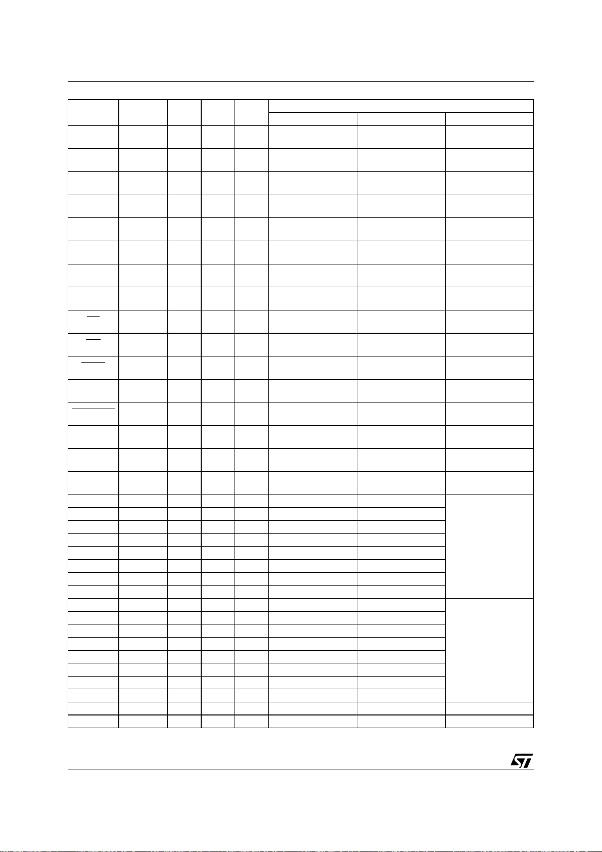
Table 5. SFR Memory Map with Direct Address and Reset Value
SFR
Addr
(hex)
80 RESERVED
81 SP SP[7:0] 07
82 DPL DPL[7:0] 00 Data
83 DPH DPH[7:0] 00
84 RESERVED
85 DPTC – AT – – – DPSEL[2:0] 00
86 DPTM – – – – MD1[1:0] MD0[1:0] 00
87 PCON SMOD0 SMOD1 – POR RCLK1 TCLK1 PD IDLE 00
88
89 TMOD GATE C/T
8A TL0 TL0[7:0] 00
8B TL1 TL1[7:0] 00
8C TH0 TH0[7:0] 00
8D TH1 TH1[7:0] 00
8E P1SFS0 P1SFS0[7:0] 00
8F P1SFS1 P1SFS1[7:0] 00
90
91 P3SFS P3SFS[7:0] 00
92 P4SFS0 P4SFS0[7:0] 00
93 P4SFS1 P4SFS1[7:0] 00
(1)
(1)
SFR
Name
TCON
P1
76 5 43210
TF1
<8Fh>
P1.7
<97h>
TR1
<8Eh>
P1.6
<96h>
Bit Name and <Bit Address> Reset
TF0
<8Dh>
M1 M0 GATE C/T M1 M0 00
P1.5
<95h>
TR0
<8Ch>
P1.4
<94h>
IE1
<8Bh>
P1.3
<93h>
IT1
<8Ah>
P1.2
<92h>
IE0
<89h>
P1.1
<91h>
IT0
<88h>
P1.0
<90h>
Value
(hex)
00
FF
with Link
Pointer
(SP), page
Pointer
(DPTR), p
age 22
13., page
14., page
26., page
41., page
42., page
Standard
SFRs, pag
31., page
32., page
27., page
30., page
34., page
35., page
Reg.
Descr.
Stack
22
Table
38
Table
39
Table
52
Table
72
Table
74
Timer
e71
Table
61
Table
61
Table
58
Table
61
Table
62
Table
62
25/264
uPSD34xx - SPECIAL FUNCTION REGISTERS (SFR)
SFR
Addr
(hex)
94 ADCPS – – – – ADCCE ADCPS[2:0] 00
95 ADAT0 ADATA[7:0] 00
96 ADAT1 – – – – – – ADATA[9:8] 00
97 ACON AINTF AINTEN ADEN ADS[2:0] ADST ADSF 00
98
99 SBUF0 SBUF0[7:0] 00
9A RESERVED
9B RESERVED
9C RESERVED
9D BUSCON EPFQ EBC WRW1 WRW0 RDW1 RDW0 CW1 CW0 EB
9E RESERVED
9F RESERVED
A0 RESERVED
A1 RESERVED
A2 PCACL0 PCACL0[7:0] 00
A3 PCACH0 PCACH0[7:0] 00
A4 PCACON0 EN_ALL EN_PCA EOVF1 PCA_IDL – – CLK_SEL[1:0] 00
A5 PCASTA OVF1 INTF5 INTF4 INTF3 OVF0 INTF2 INTF1 INTF0 00
A6 WDRST WDRST[7:0] 00
A7 IEA EADC ESPI EPCA ES1 – – EI2C – 00
(1)
SFR
Name
SCON0
76 5 43210
SM0
<9Fh>
SM1
<9Eh>
Bit Name and <Bit Address> Reset
SM2
<9Dh>
REN
<9Ch>
TB8
<9Bh>
RB8
<9Ah>TI<99h>RI<9h8>
Value
(hex)
00
Reg.
Descr.
with Link
Table
90., page
153
Table
91., page
153
Table
92., page
153
Table
89., page
152
Table
47., page
84
Figure
28., page
81
Table
37., page
65
Table
93., page
155
Table
93., page
155
Table
96., page
160
Table
98., page
162
Table
40., page
70
Table
18., page
45
26/264
uPSD34xx - SPECIAL FUNCTION REGISTERS (SFR)
SFR
Addr
(hex)
(1)
A8
A9
AA
AB
AC
AD
SFR
Name
IE
TCMMODE
0
TCMMODE
1
TCMMODE
2
CAPCOML
0
CAPCOMH
0
76 5 43210
EA
<AFh>
–
EINTF E_COMP CAP_PE CAP_NE MATCH TOGGLE PWM[1:0] 00
EINTF E_COMP CAP_PE CAP_NE MATCH TOGGLE PWM[1:0] 00
EINTF E_COMP CAP_PE CAP_NE MATCH TOGGLE PWM[1:0] 00
Bit Name and <Bit Address> Reset
ET2
<ADh>
ES0
<ACh>
ET1
<ABh>
EX1
<AAh>
ET0
<A9h>
EX0
<A8h>
CAPCOML0[7:0] 00
CAPCOMH0[7:0] 00
Value
(hex)
00
Reg.
Descr.
with Link
Table
17., page
45
Table
99., page
163
Table
93., page
155
Table
AE WDKEY WDKEY[7:0] 55
39., page
70
Table
93., page
155
Table
28., page
59
Table
93., page
155
B0
AF
(1)
B1
B2
B3
CAPCOML
1
P3
CAPCOMH
1
CAPCOML
2
CAPCOMH
2
P3.7
<B7h>
P3.6
<B6h>
P3.5
<B5h>
CAPCOML1[7:0] 00
P3.4
<B4h>
P3.3
<B3h>
P3.2
<B2h>
P3.1
<B1h>
P3.0
<B0h>
FF
CAPCOMH1[7:0] 00
CAPCOML2[7:0] 00
CAPCOMH2[7:0] 00
B4 PWMF0 PWMF0[7:0] 00
B5 RESERVED
B6 RESERVED
Table
B7 IPA PADC PSPI PPCA PS1 – – PI2C – 00
20., page
46
Table
19., page
46
B8
(1)
IP – –
PT2
<BDh>
PS0
<BCh>
PT1
<BBh>
PX1
<BAh>
PT0
<B9h>
PX0
<B8h>
00
B9 RESERVED
BA PCACL1 PCACL1[7:0] 00 Table
BB PCACH1 PCACH1[7:0] 00
93., page
155
Table
BC PCACON1 – EN_PCA EOVF1 PCA_IDL – – CLK_SEL[1:0] 00
97., page
161
27/264

uPSD34xx - SPECIAL FUNCTION REGISTERS (SFR)
SFR
Addr
(hex)
BD
BE
BF
(1)
C0
C1
C2
C3
C4
C5
C6
SFR
Name
TCMMODE
3
TCMMODE
4
TCMMODE
5
P4
CAPCOML
3
CAPCOMH
3
CAPCOML
4
CAPCOMH
4
CAPCOML
5
CAPCOMH
5
76 5 43210
EINTF E_COMP CAP_PE CAP_NE MATCH TOGGLE PWM[1:0] 00
EINTF E_COMP CAP_PE CAP_NE MATCH TOGGLE PWM[1:0] 00
EINTF E_COMP CAP_PE CAP_NE MATCH TOGGLE PWM[1:0] 00
P4.7
<C7h>
P4.6
<C6h>
Bit Name and <Bit Address> Reset
P4.5
<C5h>
P4.4
<C4h>
P4.3
<C3h>
P4.2
<C2h>
P4.1
<C1h>
P4.0
<C0h>
CAPCOML3[7:0] 00
CAPCOMH3[7:0] 00
CAPCOML4[7:0] 00
CAPCOMH4[7:0] 00
CAPCOML5[7:0] 00
CAPCOMH5[7:0] 00
C7 PWMF1 PWMF1[7:0] 00
CP/
RL2
<C8h>
C8
(1)
T2CON
TF2
<CFh>
EXF2
<CEh>
RCLK
<CDh>
TCLK
<CCh>
EXEN2
<CBh>
TR2
<CAh>
C/T2
<C9h>
C9 RESERVED
CA RCAP2L RCAP2L[7:0] 00
CB RCAP2H RCAP2H[7:0] 00
CC TL2 TL2[7:0] 00
CD TH2 TH2[7:0] 00
CE IRDACON – IRDA_EN BIT_PULS CDIV4 CDIV3 CDIV2 CDIV1 CDIV0 0F
D0
(1)
PSW
CY
<D7h>AC<D6h>F0<D5h>
RS[1:0]
<D4h, D3h>
OV
<D2h>
–
P
<D0>
D1 RESERVED
D2 SPICLKD SPICLKD[5:0] – – 04
D3 SPISTAT – – – BUSY TEISF RORISF TISF RISF 02
Value
(hex)
FF
00
00
Reg.
Descr.
with Link
Table
99., page
163
Table
29., page
59
Table
93., page
155
Table
43., page
77
Standard
Timer
SFRs, pag
e71
Table
50., page
95
Program
Status
Word
(PSW), pa
ge 23
Table
65., page
121
Table
66., page
122
28/264

uPSD34xx - SPECIAL FUNCTION REGISTERS (SFR)
SFR
Addr
(hex)
SFR
Name
76 5 43210
Bit Name and <Bit Address> Reset
Value
(hex)
Reg.
Descr.
with Link
D4 SPITDR SPITDR[7:0] 00 Table
D5 SPIRDR SPIRDR[7:0] 00
64., page
121
Table
D6 SPICON0 – TE RE SPIEN SSEL FLSB SPO – 00
63., page
120
Table
D7 SPICON1 – – – – TEIE RORIE TIE RIE 00
64., page
121
Table
48., page
85
D8
(1)
SCON1
SM0
<DF
SM1
<DE>
SM2
<DD>
REN
<DC>
TB8
<DB>
RB8
<DA>TI<D9>RI<D8>
00
Figure
D9 SBUF1 SBUF1[7:0] 00
28., page
81
DA RESERVED
Table
DB S1SETUP SS_EN SMPL_SET[6:0] 00
59., page
108
Table
DC S1CON CR2 EN1 STA STO ADDR AA CR1 CR0 00
54., page
103
Table
DD S1STA GC STOP INTR TX_MD B_BUSY B_LOST ACK_R
SLV 00
56., page
106
Table
DE S1DAT S1DAT[7:0] 00
57., page
107
Table
DF S1ADR S1ADR[7:0] 00
58., page
107
Accumulat
E0
(1)
A
<bit addresses: E7h, E6h, E5h, E4h, E3h, E2h, E1h, E0h>
A[7:0]
00
(ACC), pa
ge 22
E1 RESERVED
E2 UADDR – USBADDR[6:0] 00
E3 UPAIR – – – – PR3OUT PR1OUT PR3IN PR1IN 00
E4 UIE0 – – – – RSTIE
SUSPND
IE
EOPIE
RES
UMIE
00
E5 UIE1 – – – IN4IE IN3IE IN2IE IN1IE IN0IE 00
E6 UIE2 – – – OUT4IE OUT3IE OUT2IE OUT1IE
E7 UIE3 – – – NAK4IE NAK3IE NAK2IE NAK1IE
E8 UIF0 GLF INF OUTF NAKF RSTF
SUSPND
F
EOPF
OUT0I
E
NAK0I
E
RESU
MF
00
00
00
or
29/264
uPSD34xx - SPECIAL FUNCTION REGISTERS (SFR)
SFR
Addr
(hex)
SFR
Name
76 5 43210
Bit Name and <Bit Address> Reset
Value
(hex)
with Link
E9 UIF1 – – – IN4F IN3F IN2F IN1F IN0F 00
EA UIF2 – – – OUT4F OUT3F OUT2F OUT1F OUT0F 00
EB UIF3 – – – NAK4F NAK3F NAK2F NAK1F NAK0F 00
EC UCTL – – – – – USBEN VISIBLE
WAKE
UP
00
ED USTA – – – – RCVT SETUP IN OUT 00
EE RESERVED
EF USEL DIR – – – – EP[2:0] 00
F0
(1)
B
<bit addresses: F7h, F6h, F5h, F4h, F3h, F2h, F1h, F0h>
B[7:0]
00
B Register
(B), page
F1 UCON – – – – ENABLE STALL TOGGLE BSY 00
F2 USIZE – SIZE[6:0] 00
F3 UBASEH BASEADDR[15:8] 00
F4 UBASEL BASEADDR[7:6] 0 0 0 0 0 0 00
F5 USCI – – – – – USCI[2:0] 00
F6 USCV USCV[7:0] 00
F7 RESERVED
F8 RESERVED
F9 CCON0 PLLM[4] PLLEN UPLLCE DBGCE
CPU_
AR
CPUPS[2:0] 50
22., page
FA CCON1 PLLM[3:0] PLLD[3:0] 00
FB CCON2 – – – PCA0CE PCA0PS[3:0] 10
FC CCON3 – – – PCA1CE PCA1PS[3:0] 10
94., page
95., page
FD RESERVED
FE RESERVED
FF RESERVED
FE RESERVED
FF RESERVED
Note: 1. This SFR can be addressed by individual bits (Bit Address mode) or addressed by the entire byte (Direct Address mode).
Reg.
Descr.
22
Table
49
Table
156
Table
156
30/264

8032 ADDRESSING MODES
The 8032 MCU uses 11 different addressing
modes listed below:
■ Register
■ Direct
■ Register Indirect
■ Immediate
■ External Direct
■ External Indirect
■ Indexed
■ Relative
■ Absolute
■ Long
■ Bit
Register Addressing
This mode uses the contents of one of the registers R0 - R7 (selected by the last three bits in the
instruction opcode) as the operand source or destination. This mode is very efficient since an additional instruction byte is not needed to identify the
operand. For example:
MOV A, R7 ; Move contents of R7 to accumulator
Direct Addressing
This mode uses an 8-bit address, which is contained in the second byte of the instruction, to directly address an operand which resides in either
8032 DATA SRAM (internal address range 00h07Fh) or resides in 8032 SFR (internal address
range 80h-FFh). This mode is quite fast since the
range limit is 256 bytes of internal 8032 SRAM.
For example:
MOV A, 40h ; Move contents of DATA SRAM
; at location 40h into the accumulator
Register Indirect Addressing
This mode uses an 8-bit address contained in either Register R0 or R1 to indirectly address an operand which resides in 8032 IDATA SRAM
(internal address range 80h-FFh). Although 8032
SFR registers also occupy the same physical address range as IDATA, SFRs will not be accessed
by Register Indirect mode. SFRs may only be accesses using Direct address mode. For example:
MOV A, @R0 ; Move into the accumulator the
; contents of IDATA SRAM that is
; pointed to by the address
; contained in R0.
uPSD34xx - 8032 ADDRESSING MODES
Immediate Addressing
This mode uses 8-bits of data (a constant) contained in the second byte of the instruction, and
stores it into the memory location or register indicated by the first byte of the instruction. Thus, the
data is immediately available within the instruction.
This mode is commonly used to initialize registers
and SFRs or to perform mask operations.
There is also a 16-bit version of this mode for loading the DPTR Register. In this case, the two bytes
following the instruction byte contain the 16-bit value. For example:
MOV A, 40# ; Move the constant, 40h, into
; the accumulator
MOV DPTR, 1234# ; Move the constant, 1234h, into
; DPTR
External Direct Addressing
This mode will access external memory (XDATA)
by using the 16-bit address stored in the DPTR
Register. There are only two instructions using this
mode and both use the accumulator to either receive a byte from external memory addressed by
DPTR or to send a byte from the accumulator to
the address in DPTR. The uPSD34xx has a special feature to alternate the contents (source and
destination) of DPTR rapidly to implement very efficient memory-to-memory transfers. For example:
MOVX A, @DPTR ; Move contents of accumulator to
; XDATA at address contained in
; DPTR
MOVX @DPTR, A ; Move XDATA to accumulator
Note: See details in DUAL DATA
POINTERS, page 38.
External Indirect Addressing
This mode will access external memory (XDATA)
by using the 8-bit address stored in either Register
R0 or R1. This is the fastest way to access XDATA
(least bus cycles), but because only 8-bits are
available for address, this mode limits XDATA to a
size of only 256 bytes (the traditional Port 2 of the
8032 MCU is not available in the uPSD34xx, so it
is not possible to write the upper address byte).
This mode is not supported by uPSD34xx.
For example:
MOVX @R0,A ; Move into the accumulator the
; XDATA that is pointed to by
; the address contained in R0.
31/264

uPSD34xx - 8032 ADDRESSING MODES
Indexed Addressing
This mode is used for the MOVC instruction which
allows the 8032 to read a constant from program
memory (not data memory). MOVC is often used
to read look-up tables that are embedded in program memory. The final address produced by this
mode is the result of adding either the 16-bit PC or
DPTR value to the contents of the accumulator.
The value in the accumulator is referred to as an
index. The data fetched from the final location in
program memory is stored into the accumulator,
overwriting the index value that was previously
stored there. For example:
MOVC A, @A+DPTR; Move code byte relative to
; DPTR into accumulator
MOVC A, @A+PC ; Move code byte relative to PC
; into accumulator
Relative Addressing
This mode will add the two’s-compliment number
stored in the second byte of the instruction to the
program counter for short jumps within +128 or –
127 addresses relative to the program counter.
This is commonly used for looping and is very efficient since no additional bus cycle is needed to
fetch the jump destination address. For example:
SJMP 34h ; Jump 34h bytes ahead (in program
; memory) of the address at which
; the SJMP instruction is stored. If
; SJMP is at 1000h, program
; execution jumps to 1034h.
Absolute Addressing
This mode will append the 5 high-order bits of the
address of the next instruction to the 11 low-order
bits of an ACALL or AJUMP instruction to produce
a 16-bit jump address. The jump will be within the
same 2K byte page of program memory as the first
byte of the following instruction. For example:
AJMP 0500h ; If next instruction is located at
; address 4000h, the resulting jump
; will be made to 4500h.
Long Addressing
This mode will use the 16-bits contained in the two
bytes following the instruction byte as a jump destination address for LCALL and LJMP instructions.
For example:
LJMP 0500h ; Unconditionally jump to address
; 0500h in program memory
Bit Addressing
This mode allows setting or clearing an individual
bit without disturbing the other bits within an 8-bit
value of internal SRAM. Bit Addressing is only
available for certain locations in 8032 DATA and
SFR memory. Valid locations are DATA addresses 20h - 2Fh and for SFR addresses whose base
address ends with 0h or 8h. (Example: The SFR,
IE, has a base address of A8h, so each of the eight
bits in IE can be addressed individually at address
A8h, A9h, ...up to AFh.) For example:
SETB AFh ; Set the individual EA bit (Enable All
; Interrupts) inside the SFR Register,
; IE.
32/264

uPSD34xx - uPSD34xx INSTRUCTION SET SUMMARY
uPSD34xx INSTRUCTION SET SUMMARY
Tables 6 through 11 list all of the instructions supported by the uPSD34xx, including the number of
bytes and number of machine cycles required to
implement each instruction. This is the standard
8051 instruction set.
The meaning of “machine cycles” is how many
8032 MCU core machine cycles are required to
execute the instruction. The “native” duration of all
machine cycles is set by the memory wait state
settings in the SFR, BUSCON, and the MCU clock
divider selections in the SFR, CCON0 (i.e. a machine cycle is typically set to 4 MCU clocks for a 5V
uPSD34xx). However, an individual machine cycle
may grow in duration when either of two things
happen:
Table 6. Arithmetic Instruction Set
Mnemonic
ADD A, Rn Add register to ACC 1 byte/1 cycle
ADD A, Direct Add direct byte to ACC 2 byte/1 cycle
ADD A, @Ri Add indirect SRAM to ACC 1 byte/1 cycle
ADD A, #data Add immediate data to ACC 2 byte/1 cycle
ADDC A, Rn Add register to ACC with carry 1 byte/1 cycle
ADDC A, direct Add direct byte to ACC with carry 2 byte/1 cycle
ADDC A, @Ri Add indirect SRAM to ACC with carry 1 byte/1 cycle
ADDC A, #data Add immediate data to ACC with carry 2 byte/1 cycle
SUBB A, Rn Subtract register from ACC with borrow 1 byte/1 cycle
SUBB A, direct Subtract direct byte from ACC with borrow 2 byte/1 cycle
SUBB A, @Ri Subtract indirect SRAM from ACC with borrow 1 byte/1 cycle
SUBB A, #data Subtract immediate data from ACC with borrow 2 byte/1 cycle
INC A Increment A 1 byte/1 cycle
INC Rn Increment register 1 byte/1 cycle
INC direct Increment direct byte 2 byte/1 cycle
INC @Ri Increment indirect SRAM 1 byte/1 cycle
DEC A Decrement ACC 1 byte/1 cycle
DEC Rn Decrement register 1 byte/1 cycle
DEC direct Decrement direct byte 2 byte/1 cycle
DEC @Ri Decrement indirect SRAM 1 byte/1 cycle
INC DPTR Increment Data Pointer 1 byte/2 cycle
MUL AB Multiply ACC and B 1 byte/4 cycle
DIV AB Divide ACC by B 1 byte/4 cycle
DA A Decimal adjust ACC 1 byte/1 cycle
Note: 1. All mnemonics copyrighted ©Intel Corporation 1980.
(1)
and Use
1. a stall is imposed while loading the 8032 PreFetch Queue (PFQ); or
2. the occurrence of a cache miss in the Branch
Cache (BC) during a branch in program
execution flow.
See 8032 MCU CORE PERFORMANCE
ENHANCEMENTS, page 18 or more details.
But generally speaking, during typical program execution, the PFQ is not empty and the BC has no
misses, producing very good performance without
extending the duration of any machine cycles.
The uPSD34xx Programmers Guide describes
each instruction operation in detail.
Description Length/Cycles
33/264

uPSD34xx - uPSD34xx INSTRUCTION SET SUMMARY
Table 7. Logical Instruction Set
Mnemonic
ANL A, Rn AND register to ACC 1 byte/1 cycle
ANL A, direct AND direct byte to ACC 2 byte/1 cycle
ANL A, @Ri AND indirect SRAM to ACC 1 byte/1 cycle
ANL A, #data AND immediate data to ACC 2 byte/1 cycle
ANL direct, A AND ACC to direct byte 2 byte/1 cycle
ANL direct, #data AND immediate data to direct byte 3 byte/2 cycle
ORL A, Rn OR register to ACC 1 byte/1 cycle
ORL A, direct OR direct byte to ACC 2 byte/1 cycle
ORL A, @Ri OR indirect SRAM to ACC 1 byte/1 cycle
ORL A, #data OR immediate data to ACC 2 byte/1 cycle
ORL direct, A OR ACC to direct byte 2 byte/1 cycle
ORL direct, #data OR immediate data to direct byte 3 byte/2 cycle
SWAP A Swap nibbles within the ACC 1 byte/1 cycle
XRL A, Rn Exclusive-OR register to ACC 1 byte/1 cycle
XRL A, direct Exclusive-OR direct byte to ACC 2 byte/1 cycle
XRL A, @Ri Exclusive-OR indirect SRAM to ACC 1 byte/1 cycle
XRL A, #data Exclusive-OR immediate data to ACC 2 byte/1 cycle
XRL direct, A Exclusive-OR ACC to direct byte 2 byte/1 cycle
XRL direct, #data Exclusive-OR immediate data to direct byte 3 byte/2 cycle
CLR A Clear ACC 1 byte/1 cycle
CPL A Compliment ACC 1 byte/1 cycle
RL A Rotate ACC left 1 byte/1 cycle
RLC A Rotate ACC left through the carry 1 byte/1 cycle
RR A Rotate ACC right 1 byte/1 cycle
RRC A Rotate ACC right through the carry 1 byte/1 cycle
Note: 1. All mnemonics copyrighted ©Intel Corporation 1980.
(1)
and Use
Logical Instructions
Description Length/Cycles
34/264

uPSD34xx - uPSD34xx INSTRUCTION SET SUMMARY
Table 8. Data Transfer Instruction Set
Mnemonic
MOV A, Rn Move register to ACC 1 byte/1 cycle
MOV A, direct Move direct byte to ACC 2 byte/1 cycle
MOV A, @Ri Move indirect SRAM to ACC 1 byte/1 cycle
MOV A, #data Move immediate data to ACC 2 byte/1 cycle
MOV Rn, A Move ACC to register 1 byte/1 cycle
MOV Rn, direct Move direct byte to register 2 byte/2 cycle
MOV Rn, #data Move immediate data to register 2 byte/1 cycle
MOV direct, A Move ACC to direct byte 2 byte/1 cycle
MOV direct, Rn Move register to direct byte 2 byte/2 cycle
MOV direct, direct Move direct byte to direct 3 byte/2 cycle
MOV direct, @Ri Move indirect SRAM to direct byte 2 byte/2 cycle
MOV direct, #data Move immediate data to direct byte 3 byte/2 cycle
MOV @Ri, A Move ACC to indirect SRAM 1 byte/1 cycle
MOV @Ri, direct Move direct byte to indirect SRAM 2 byte/2 cycle
MOV @Ri, #data Move immediate data to indirect SRAM 2 byte/1 cycle
MOV DPTR, #data16 Load Data Pointer with 16-bit constant 3 byte/2 cycle
MOVC A, @A+DPTR Move code byte relative to DPTR to ACC 1 byte/2 cycle
MOVC A, @A+PC Move code byte relative to PC to ACC 1 byte/2 cycle
MOVX A, @Ri Move XDATA (8-bit addr) to ACC 1 byte/2 cycle
MOVX A, @DPTR Move XDATA (16-bit addr) to ACC 1 byte/2 cycle
MOVX @Ri, A Move ACC to XDATA (8-bit addr) 1 byte/2 cycle
MOVX @DPTR, A Move ACC to XDATA (16-bit addr) 1 byte/2 cycle
XCH A, Rn Exchange register with ACC 1 byte/1 cycle
PUSH direct Push direct byte onto stack 2 byte/2 cycle
POP direct Pop direct byte from stack 2 byte/2 cycle
XCH A, direct Exchange direct byte with ACC 2 byte/1 cycle
XCH A, @Ri Exchange indirect SRAM with ACC 1 byte/1 cycle
XCHD A, @Ri Exchange low-order digit indirect SRAM with ACC 1 byte/1 cycle
Note: 1. All mnemonics copyrighted ©Intel Corporation 1980.
(1)
and Use
Description Length/Cycles
35/264
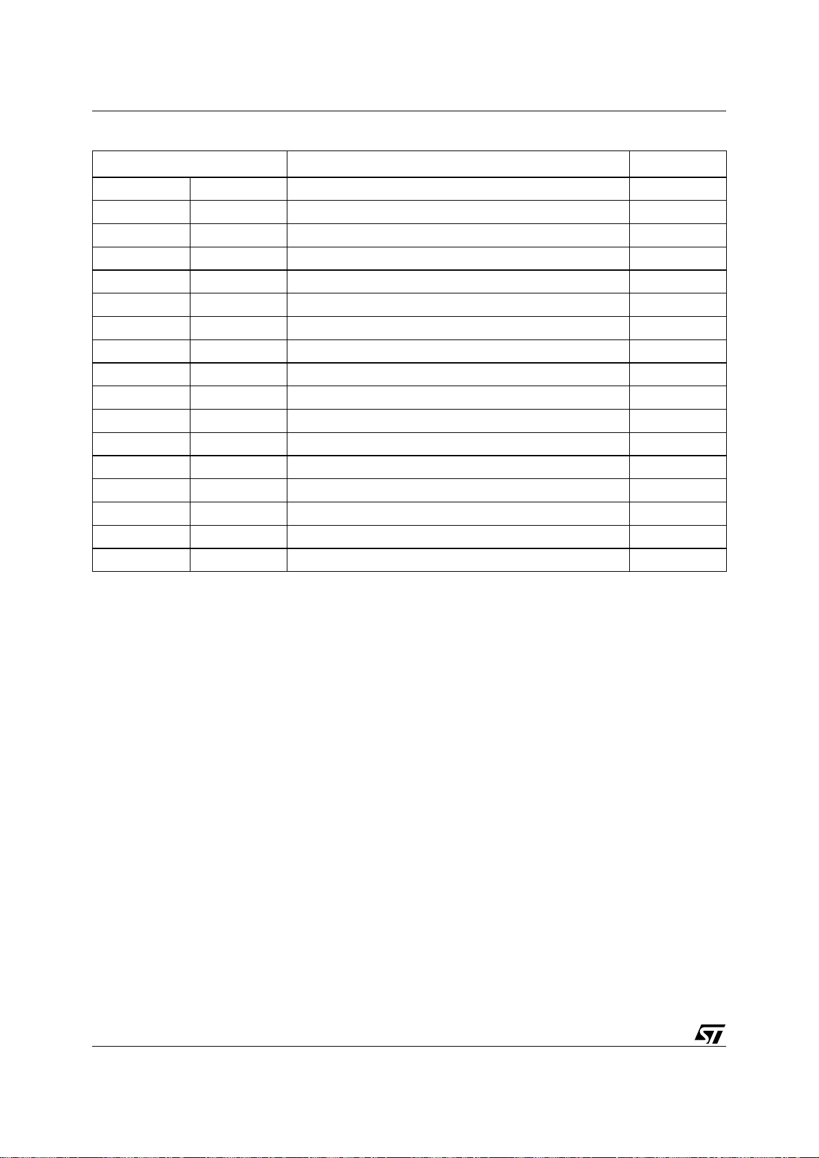
uPSD34xx - uPSD34xx INSTRUCTION SET SUMMARY
Table 9. Boolean Variable Manipulation Instruction Set
Mnemonic
CLR C Clear carry 1 byte/1 cycle
CLR bit Clear direct bit 2 byte/1 cycle
SETB C Set carry 1 byte/1 cycle
SETB bit Set direct bit 2 byte/1 cycle
CPL C Compliment carry 1 byte/1 cycle
CPL bit Compliment direct bit 2 byte/1 cycle
ANL C, bit AND direct bit to carry 2 byte/2 cycle
ANL C, /bit AND compliment of direct bit to carry 2 byte/2 cycle
ORL C, bit OR direct bit to carry 2 byte/2 cycle
ORL C, /bit OR compliment of direct bit to carry 2 byte/2 cycle
MOV C, bit Move direct bit to carry 2 byte/1 cycle
MOV bit, C Move carry to direct bit 2 byte/2 cycle
JC rel Jump if carry is set 2 byte/2 cycle
JNC rel Jump if carry is not set 2 byte/2 cycle
JB rel Jump if direct bit is set 3 byte/2 cycle
JNB rel Jump if direct bit is not set 3 byte/2 cycle
JBC bit, rel Jump if direct bit is set and clear bit 3 byte/2 cycle
Note: 1. All mnemonics copyrighted ©Intel Corporation 1980.
(1)
and Use
Description Length/Cycles
36/264
uPSD34xx - uPSD34xx INSTRUCTION SET SUMMARY
Table 10. Program Branching Instruction Set
Mnemonic
ACALL addr11 Absolute subroutine call 2 byte/2 cycle
LCALL addr16 Long subroutine call 3 byte/2 cycle
RET Return from subroutine 1 byte/2 cycle
RETI Return from interrupt 1 byte/2 cycle
AJMP addr11 Absolute jump 2 byte/2 cycle
LJMP addr16 Long jump 3 byte/2 cycle
SJMP rel Short jump (relative addr) 2 byte/2 cycle
JMP @A+DPTR Jump indirect relative to the DPTR 1 byte/2 cycle
JZ rel Jump if ACC is zero 2 byte/2 cycle
JNZ rel Jump if ACC is not zero 2 byte/2 cycle
CJNE A, direct, rel Compare direct byte to ACC, jump if not equal 3 byte/2 cycle
CJNE A, #data, rel Compare immediate to ACC, jump if not equal 3 byte/2 cycle
CJNE Rn, #data, rel Compare immediate to register, jump if not equal 3 byte/2 cycle
CJNE @Ri, #data, rel Compare immediate to indirect, jump if not equal 3 byte/2 cycle
DJNZ Rn, rel Decrement register and jump if not zero 2 byte/2 cycle
DJNZ direct, rel Decrement direct byte and jump if not zero 3 byte/2 cycle
Note: 1. All mnemonics copyrighted ©Intel Corporation 1980.
(1)
and Use
Program Branching Instructions
Description Length/Cycles
Table 11. Miscellaneous Instruction Set
Mnemonic
NOP No Operation 1 byte/1 cycle
Note: 1. All mnemonics copyrighted ©Intel Corporation 1980.
(1)
and Use
Miscellaneous
Description Length/Cycles
Table 12. Notes on Instruction Set and Addressing Modes
Rn Register R0 - R7 of the currently selected register bank.
direct 8-bit address for internal 8032 DATA SRAM (locations 00h - 7Fh) or SFR registers (locations 80h - FFh).
@Ri 8-bit internal 8032 SRAM (locations 00h - FFh) addressed indirectly through contents of R0 or R1.
#data 8-bit constant included within the instruction.
#data16 16-bit constant included within the instruction.
addr16 16-bit destination address used by LCALL and LJMP.
addr11 11-bit destination address used by ACALL and AJMP.
rel Signed (two-s compliment) 8-bit offset byte.
bit
Direct addressed bit in internal 8032 DATA SRAM (locations 20h to 2Fh) or in SFR registers (88h, 90h,
98h, A8h, B0, B8h, C0h, C8h, D0h, D8h, E0h, F0h).
37/264
uPSD34xx - DUAL DATA POINTERS
DUAL DATA POINTERS
XDATA is accessed by the External Direct addressing mode, which uses a 16-bit address
stored in the DPTR Register. Traditional 8032 architecture has only one DPTR Register. This is a
burden when transferring data between two XDATA locations because it requires heavy use of the
working registers to manipulate the source and
destination pointers.
However, the uPSD34xx has two data pointers,
one for storing a source address and the other for
storing a destination address. These pointers can
be configured to automatically increment or decrement after each data transfer, further reducing the
burden on the 8032 and making this kind of data
movement very efficient.
Data Pointer Control Register, DPTC (85h)
By default, the DPTR Register of the uPSD34xx
will behave no different than in a standard 8032
MCU. The DPSEL0 Bit of SFR register DPTC
shown in Table 13, selects which one of the two
“background” data pointer registers (DPTR0 or
DPTR1) will function as the traditional DPTR Reg-
ister at any given time. After reset, the DPSEL0 Bit
is cleared, enabling DPTR0 to function as the DPTR, and firmware may access DPTR0 by reading
or writing the traditional DPTR Register at SFR addresses 82h and 83h. When the DPSEL0 bit is set,
then the DPTR1 Register functions as DPTR, and
firmware may now access DPTR1 through SFR
registers at 82h and 83h. The pointer which is not
selected by the DPSEL0 bit remains in the background and is not accessible by the 8032. If the
DPSEL0 bit is never set, then the uPSD34xx will
behave like a traditional 8032 having only one
DPTR Register.
To further speed XDATA to XDATA transfers, the
SFR bit, AT, may be set to automatically toggle the
two data pointers, DPTR0 and DPTR1, each time
the standard DPTR Register is accessed by a
MOVX instruction. This eliminates the need for
firmware to manually manipulate the DPSEL0 bit
between each data transfer.
Detailed description for the SFR register DPTC is
shown in Table 13.
Table 13. DPTC: Data Pointer Control Register (SFR 85h, reset value 00h)
Bit 7Bit 6Bit 5Bit 4Bit 3Bit 2Bit 1Bit 0
–AT–––––DPSEL0
Details
Bit Symbol R/W Definition
7 – – Reserved
6ATR,W
5-1 – – Reserved
0 DPSE0 R,W
0 = Manually Select Data Pointer
1 = Auto Toggle between DPTR0 and DPTR1
0 = DPTR0 Selected for use as DPTR
1 = DPTR1 Selected for use as DPTR
38/264
uPSD34xx - DUAL DATA POINTERS
Data Pointer Mode Register, DPTM (86h)
The two “background” data pointers, DPTR0 and
DPTR1, can be configured to automatically increment, decrement, or stay the same after a MOVX
instruction accesses the DPTR Register. Only the
currently selected pointer will be affected by the increment or decrement. This feature is controlled
by the DPTM Register defined in Table 14.
The automatic increment or decrement function is
effective only for the MOVX instruction, and not
MOVC or any other instruction that uses the DTPR
Register.
Table 14. DPTM: Data Pointer Mode Register (SFR 86h, reset value 00h)
Bit 7Bit 6Bit 5Bit 4Bit 3Bit 2Bit 1Bit 0
– – – – MD11 MD10 MD01 MD00
Details
Bit Symbol R/W Definition
7-4 – – Reserved
DPTR1 Mode Bits
Firmware Example. The 8051 assembly code illustrated in Table 15 shows how to transfer a block
of data bytes from one XDATA address region to
another XDATA address region. Auto-address incrementing and auto-pointer toggling will be used.
3-2 MD[11:10] R,W
1-0 MD[01:00] R,W
00: DPTR1 No Change
01: Reserved
10: Auto Increment
11: Auto Decrement
DPTR0 Mode Bits
00: DPTR0 No Change
01: Reserved
10: Auto Increment
11: Auto Decrement
Table 15. 8051 Assembly Code Example
MOV R7, #COUNT ; initialize size of data block to transfer
MOV DPTR, #SOURCE_ADDR ; load XDATA source address base into DPTR0
MOV 85h, #01h ; load DPTC to access DPTR1 pointer
MOV DPTR, #DEST_ADDR ; load XDATA destination address base into DPTR1
MOV 85h, #40h ; load DPTC to access DPTR0 pointer and auto toggle
MOV 86h, #0Ah ; load DPTM to auto-increment both pointers
LOOP:
Note: 1. The code loop where the data transfer takes place is only 3 lines of code.
(1)
MOVX
(1)
MOVX
(1)
DJNZ
MOV 86h, #00 ; disable auto-increment
MOV 85h, #00 ; disable auto-toggle, now back to single DPTR mode
A, @DPTR ; load XDATA byte from source into ACC.
; after load completes, DPTR0 increments and DPTR
; switches DPTR1
@DPTR, A ; store XDATA byte from ACC to destination.
; after store completes, DPTR1 increments and DPTR
; switches to DPTR0
R7, LOOP ; continue until done
39/264

uPSD34xx - DEBUG UNIT
DEBUG UNIT
The 8032 MCU Module supports run-time debugging through the JTAG interface. This same JTAG
interface is also used for In-System Programming
(ISP) and the physical connections are described
in the PSD Module section, JTAG ISP and JTAG
Debug, page 226.
Debugging with a serial interface such as JTAG is
a non-intrusive way to gain access to the internal
state of the 8032 MCU core and various memories. A traditional external hardware emulator cannot be completely effective on the uPSD34xx
because of the Pre-Fetch Queue and Branch
Cache. The nature of the PFQ and BC hide the
visibility of actual program flow through traditional
external bus connections, thus requiring on-chip
serial debugging instead.
Debugging is supported by Windows PC based
software tools used for 8051 code development
from 3rd party vendors listed at www.st.com/psm.
Debug capabilities include:
■ Halt or Start MCU execution
■ Reset the MCU
■ Single Step
■ 3 Match Breakpoints
■ 1 Range Breakpoint (inside or outside range)
■ Program Tracing
■ Read or Modify MCU core registers, DATA,
IDATA, SFR, XDATA, and Code
■ External Debug Event Pin, Input or Output
Some key points regarding use of the JTAG Debugger.
– The JTAG Debugger can access MCU
registers, data memory, and code memory
while the MCU is executing at full speed by
cycle-stealing. This means “watch windows”
may be displayed and periodically updated on
the PC during full speed operation. Registers
and data content may also be modified during
full speed operation.
– There is no on-chip storage for Program Trace
data, but instead this data is scanned from the
uPSD34xx through the JTAG channel at runtime to the PC host for proccessing. As such,
full speed program tracing is possible only
when the 8032 MCU is operating below
approximately one MIPS of performance.
Above one MIPS, the program will not run
real-time while tracing. One MIPS
performance is determined by the
combination of choice for MCU clock
frequency, and the bit settings in SFR
registers BUSCON and CCON0.
– Breakpoints can optionally halt the MCU, and/
or assert the external Debug Event pin.
– Breakpoint definitions may be qualified with
read or write operations, and may also be
qualified with an address of code, SFR, DATA,
IDATA, or XDATA memories.
– Three breakpoints will compare an address,
but the fourth breakpoint can compare an
address and also data content. Additionally,
the fouth breakpoint can be logically combined
(AND/OR) with any of the other three
breakpoints.
– The Debug Event pin can be configured by the
PC host to generate an output pulse for
external triggering when a break condition is
met. The pin can also be configured as an
event input to the breakpoint logic, causing a
break on the falling-edge of an external event
signal. If not used, the Debug Event pin should
be pulled up to V
as described in the
CC
section, Debugging the 8032 MCU
Module., page 232.
– The duration of a pulse, generated when the
Event pin configured as an output, is one MCU
clock cycle. This is an active-low signal, so the
first edge when an event occurs is high-to-low.
– The clock to the Watchdog Timer, ADC, and
2
C interface are not stopped by a breakpoint
I
halt.
– The Watchdog Timer should be disabled while
debugging with JTAG, else a reset will be
generated upon a watchdog time-out.
40/264

INTERRUPT SYSTEM
The uPSD34xx has an 12-source, two priority level
interrupt structure summarized in Table 16.
Firmware may assign each interrupt source either
high or low priority by writing to bits in the SFRs
named, IP and IPA, shown in Table 16. An interrupt will be serviced as long as an interrupt of
equal or higher priority is not already being serviced. If an interrupt of equal or higher priority is
being serviced, the new interrupt will wait until it is
finished before being serviced. If a lower priority
interrupt is being serviced, it will be stopped and
the new interrupt is serviced. When the new interrupt is finished, the lower priority interrupt that was
stopped will be completed. If new interrupt requests are of the same priority level and are received simultaneously, an internal polling
sequence determines which request is selected
for service. Thus, within each of the two priority
levels, there is a second priority structure determined by the polling sequence.
Firmware may individually enable or disable interrupt sources by writing to bits in the SFRs named,
IE and IEA, shown in Table 16., page 42. The SFR
named IE contains a global disable bit (EA), which
can be cleared to disable all 12 interrupts at once,
as shown in Table 17., page 45. Figure
13., page 43 illustrates the interrupt priority, poll-
ing, and enabling process.
Each interrupt source has at least one interrupt
flag that indicates whether or not an interrupt is
pending. These flags reside in bits of various
SFRs shown in Table 16., page 42.
All of the interrupt flags are latched into the interrupt control system at the beginning of each MCU
machine cycle, and they are polled at the beginning of the following machine cycle. If polling determines one of the flags was set, the interrupt
control system automatically generates an LCALL
to the user’s Interrupt Service Routine (ISR) firmware stored in program memory at the appropriate
vector address.
uPSD34xx - INTERRUPT SYSTEM
The specific vector address for each of the interrupt sources are listed in Table 16., page 42. However, this LCALL jump may be blocked by any of
the following conditions:
– An interrupt of equal or higher priority is
already in progress
– The current machine cycle is not the final cycle
in the execution of the instruction in progress
– The current instruction involves a write to any
of the SFRs: IE, IEA, IP, or IPA
– The current instruction is an RETI
Note: Interrupt flags are polled based on a sample
taken in the previous MCU machine cycle. If an interrupt flag is active in one cycle but is denied serviced due to the conditions above, and then later it
is not active when the conditions above are finally
satisfied, the previously denied interrupt will not be
serviced. This means that active interrupts are not
remembered. Every poling cycle is new.
Assuming all of the listed conditions are satisfied,
the MCU executes the hardware generated
LCALL to the appropriate ISR. This LCALL pushes
the contents of the PC onto the stack (but it does
not save the PSW) and loads the PC with the appropriate interrupt vector address. Program execution then jumps to the ISR at the vector address.
Execution precedes in the ISR. It may be necessary for the ISR firmware to clear the pending interrupt flag for some interrupt sources, because
not all interrupt flags are automatically cleared by
hardware when the ISR is called, as shown in Ta-
ble 16., page 42. If an interrupt flag is not cleared
after servicing the interrupt, an unwanted interrupt
will occur upon exiting the ISR.
After the interrupt is serviced, the last instruction
executed by the ISR is RETI. The RETI informs
the MCU that the ISR is no longer in progress and
the MCU pops the top two bytes from the stack
and loads them into the PC. Execution of the interrupted program continues where it left off.
Note: An ISR must end with a RETI instruction,
not a RET. An RET will not inform the interrupt
control system that the ISR is complete, leaving
the MCU to think the ISR is still in progress, making future interrupts impossible.
41/264

uPSD34xx - INTERRUPT SYSTEM
Table 16. Interrupt Summary
Enable Bit Name
(SFR.bit position)
1 = Intr Enabled
0 = Intr Disabled
Interrupt
Source
Polling
Priority
Vector
Addr
Flag Bit Name
(SFR.bit position)
1 = Intr Pending
0 = No Interrupt
Flag Bit Auto-
Cleared
by Hardware?
Reserved 0 (high) 0063h – – – –
External
Interrupt INT0
Timer 0
Overflow
External
Interrupt INT1
Timer 1
Overflow
1 0003h IE0 (TCON.1)
2 000Bh TF0 (TCON.5) Yes ET0 (IE.1) PT0 (IP.1)
3 0013h IE1 (TCON.3
4 001Bh TF1 (TCON.7) Yes ET1 (IE.3) PT1 (IP.3)
UART0 5 0023h
Timer 2
Overflow
6 002Bh
or TX2 Pin
RI (SCON0.0)
TI (SCON0.1)
TF2 (T2CON.7)
EXF2 (T2CON.6)
Edge - Yes
Level - No
Edge - Yes
Level - No
EX0 (IE.0) PX0 (IP.0)
EX1 (IE.2) PX1 (IP.2)
No ES0 (IE.4) PS0 (IP.4)
No ET2 (IE.5) PT2 (IP.5)
TEISF, RORISF,
SPI 7 0053h
TISF, RISF
Yes ESPI (IEA.6) PSPI (IPA.6)
(SPISTAT[3:0])
USB 8 0033h
2
I
C
9 0043h INTR (S1STA.5) Yes
(1)
–
No EUSB (IEA.0) PUSB (IPA.0)
EI2C (IEA.1) PI2C (IPA.1)
ADC 10 003Bh AINTF (ACON.7) No EADC (IEA.7) PADC (IPA.7)
PCA 11 005Bh
UART1 12 (low) 004Bh
Note: 1. See USB interrupt flag registers UIF0-3.
OFVx, INTFx
(PCASTA[0:7])
RI (SCON1.0)
TI (SCON1.1)
No EPCA (IEA.5) PPCA (IPA.5)
No ES1 (IEA.4) PS1 (IPA.4)
Priority Bit Name
(SFR.bit position)
1= High Priority
0 = Low Priority
42/264

Figure 13. Enabling and Polling Interrupts
uPSD34xx - INTERRUPT SYSTEM
Interrupt
Sources
Reserved
Ext
INT0
Timer 0
Ext
INT1
Timer 1
UART0
Timer 2
SPI
USB
IE/IEA
Priority
IP/IPA
High
Low
Interrupt Polling
Sequence
2
I
C
ADC
PCA
UART1
Global
Enable
AI07844
43/264

uPSD34xx - INTERRUPT SYSTEM
Individual Interrupt Sources
External Interrupts Int0 and Int1. External in-
terrupt inputs on pins EXTINT0 and EXTINT1
(pins 3.2 and 3.3) are either edge-triggered or level-triggered, depending on bits IT0 and IT1 in the
SFR named TCON.
When an external interrupt is generated from an
edge-triggered (falling-edge) source, the appropriate flag bit (IE0 or IE1) is automatically cleared by
hardware upon entering the ISR.
When an external interrupt is generated from a
level-triggered (low-level) source, the appropriate
flag bit (IE0 or IE1) is NOT automatically cleared
by hardware.
Timer 0 and 1 Overflow Interrupt. Timer 0 and
Timer 1 interrupts are generated by the flag bits
TF0 and TF1 when there is an overflow condition
in the respective Timer/Counter register (except
for Timer 0 in Mode 3).
Timer 2 Overflow Interrupt. This interrupt is
generated to the MCU by a logical OR of flag bits,
TF2 and EXE2. The ISR must read the flag bits to
determine the cause of the interrupt.
– TF2 is set by an overflow of Timer 2.
– EXE2 is generated by the falling edge of a
signal on the external pin, T2X (pin P1.1).
UART0 and UART1 Interrupt. Each of the
UARTs have identical interrupt structure. For each
UART, a single interrupt is generated to the MCU
by the logical OR of the flag bits, RI (byte received)
and TI (byte transmitted).
The ISR must read flag bits in the SFR named
SCON0 for UART0, or SCON1 for UART1 to determine the cause of the interrupt.
SPI Interrupt. The SPI interrupt has four interrupt
sources, which are logically ORed together when
interrupting the MCU. The ISR must read the flag
bits to determine the cause of the interrupt.
A flag bit is set for: end of data transmit (TEISF);
data receive overrun (RORISF); transmit buffer
empty (TISF); or receive buffer full (RISF).
2
C Interrupt. The flag bit INTR is set by a variety
I
of conditions occurring on the I
2
C interface: received own slave address (ADDR flag); received
general call address (GC flag); received STOP
condition (STOP flag); or successful transmission
or reception of a data byte.The ISR must read the
flag bits to determine the cause of the interrupt.
ADC Interrupt. The flag bit AINTF is set when an
A-to-D conversion has completed.
PCA Interrupt. The PCA has eight interrupt
sources, which are logically ORed together when
interrupting the MCU.The ISR must read the flag
bits to determine the cause of the interrupt.
– Each of the six TCMs can generate a "match
or capture" interrupt on flag bits OFV5..0
respectively.
– Each of the two 16-bit counters can generate
an overflow interrupt on flag bits INTF1 and
INTF0 respectively.
Tables 17 through Table 20., page 46 have detailed bit definitions of the interrupt system SFRs.
USB Interrupt. The USB interrupt has multiple
sources. The ISR must read the USB Interrupt
Flag Registers (UIF0-3) to determine the source of
the interrupt.
The USB interrupt can be activated by any of the
following four group of interrupt sources:
– Global: the interrupt flag is set when any of the
following events occurs: USB Reset, USB
Suspend, USB Resume, and End of Packet;
– In FIFO: the interrupt flag is set when any of
the End Point In FIFO becomes empty;
– Out FIFO: the interrupt flag is set when any of
the End Point Out FIFO becomes full; and
– In FIFO NAK: the interrupt flag is set when any
of the End Point In FIFO is not ready for an IN
(in-bound) packet.
44/264

uPSD34xx - INTERRUPT SYSTEM
Table 17. IE: Interrupt Enable Register (SFR A8h, reset value 00h)
Bit 7Bit 6Bit 5Bit 4Bit 3Bit 2Bit 1Bit 0
EA – ET2 ES0 ET1 EX1 ET0 EX0
Details
Bit Symbol R/W Function
7EAR,W
6–R,W
(1)
5
(1)
4
(1)
3
(1)
2
(1)
1
(1)
0
Note: 1. 1 = Enable Interrupt, 0 = Disable Interrupt
ET2 R,W Enable Timer 2 Interrupt
ES0 R,W Enable UART0 Interrupt
ET1 R,W Enable Timer 1 Interrupt
EX1 R,W Enable External Interrupt INT1
ET0 R,W Enable Timer 0 Interrupt
EX0 R,W Enable External Interrupt INT0
Global disable bit. 0 = All interrupts are disabled. 1 = Each interrupt
source can be individually enabled or disabled by setting or clearing its
enable bit.
Do not modify this bit. It is used by the JTAG debugger for instruction
tracing. Always read the bit and write back the same bit value when
writing this SFR.
Table 18. IEA: Interrupt Enable Addition Register (SFR A7h, reset value 00h)
Bit 7Bit 6Bit 5Bit 4Bit 3Bit 2Bit 1Bit 0
EADC ESPI EPCA ES1 – –
Details
Bit Symbol R/W Function
(1)
7
(1)
6
(1)
5
(1)
4
EADC R,W Enable ADC Interrupt
ESPI R,W Enable SPI Interrupt
EPCA R,W Enable Programmable Counter Array Interrupt
ES1 R,W Enable UART1 Interrupt
3 – – Reserved, do not set to logic '1.'
2 – – Reserved, do not set to logic '1.'
(1)
1
EI2C
R,W
Enable I2C Interrupt
0 EUSB R,W Enable USB Interrupt
Note: 1. 1 = Enable Interrupt, 0 = Disable Interrupt
EI
2
C
EUSB
45/264

uPSD34xx - INTERRUPT SYSTEM
Table 19. IP: Interrupt Priority Register (SFR B8h, reset value 00h)
Bit 7Bit 6Bit 5Bit 4Bit 3Bit 2Bit 1Bit 0
– – PT2 PS0 PT1 PX1 PT0 PX0
Details
Bit Symbol R/W Function
7 – – Reserved
6 – – Reserved
(1)
5
(1)
4
(1)
3
(1)
2
(1)
1
(1)
0
Note: 1. 1 = Assigns high priority level, 0 = Assigns low priority level
Table 20. IPA: Interrupt Priority Addition register (SFR B7h, reset value 00h)
Bit 7Bit 6Bit 5Bit 4Bit 3Bit 2Bit 1Bit 0
PADC PSPI PPCA PS1 – –
Details
Bit Symbol R/W Function
(1)
7
(1)
6
(1)
5
(1)
4
3 – – Reserved
2 – – Reserved
(1)
1
0 PUSB R,W USB Interrupt priority level
Note: 1. 1 = Assigns high priority level, 0 = Assigns low priority level
PT2 R,W Timer 2 Interrupt priority level
PS0 R,W UART0 Interrupt priority level
PT1 R,W Timer 1 Interrupt priority level
PX1 R,W External Interrupt INT1 priority level
PT0 R,W Timer 0 Interrupt priority level
PX0 R,W External Interrupt INT0 priority level
PADC R,W ADC Interrupt priority level
PSPI R,W SPI Interrupt priority level
PPCA R,W PCA Interrupt level
PS1 R,W UART1 Interrupt priority level
PI2C
R,W
I2C Interrupt priority level
PI
2
C
PUSB
46/264

MCU CLOCK GENERATION
Internal system clocks generated by the clock generation unit are derived from the signal, XTAL1,
shown in Figure 14. XTAL1 has a frequency f
which comes directly from the external crystal or
oscillator device. The SFR named CCON0 (Table
22., page 49) controls the clock generation unit.
There are two clock signals produced by the clock
generation unit:
■ MCU_CLK
■ PERIPH_CLK
MCU_CLK
This clock drives the 8032 MCU core and the
Watchdog Timer (WDT). The frequency of
MCU_CLK is equal to f
by default, but it can be
OSC
divided by as much as 2048, shown in Figure 14.
The bits CPUPS[2:0] select one of eight different
divisors, ranging from 2 to 2048. The new frequency is available immediately after the CPUPS[2:0]
bits are written. The final frequency of MCU_CLK
MCU
.
is f
MCU_CLK is blocked by either bit, PD or IDL, in
the SFR named PCON during MCU Power-down
Mode or Idle Mode respectively.
MCU_CLK clock can be further divided as required for use in the WDT. See details of the WDT
in SUPERVISORY FUNCTIONS, page 67.
PERIPH_CLK
This clock drives all the uPSD34xx peripherals except the WDT. The Frequency of PERIPH_CLK is
always f
. Each of the peripherals can indepen-
OSC
dently divide PERIPH_CLK to scale it appropriately for use.
PERIPH_CLK runs at all times except when
blocked by the PD bit in the SFR named PCON
during MCU Power-down Mode.
JTAG Interface Clock. The JTAG interface for
ISP and for Debugging uses the externally supplied JTAG clock, coming in on pin TCK. This
means the JTAG ISP interface is always available,
and the JTAG Debug interface is available when
enabled, even during MCU Idle mode and Powerdown Mode.
However, since the MCU participates in the JTAG
debug process, and MCU_CLK is halted during
Idle and Power-down Modes, the majority of debug functions are not available during these low
power modes. But the JTAG debug interface is capable of executing a reset command while in these
low power modes, which will exit back to normal
OSC
uPSD34xx - MCU CLOCK GENERATION
operating mode where all debug commands are
available again.
,
The CCON0 SFR contains a bit, DBGCE, which
enables the breakpoint comparators inside the
JTAG Debug Unit when set. DBGCE is set by default after reset, and firmware may clear this bit at
run-time. Disabling these comparators will reduce
current consumption on the MCU Module, and it is
recommended to do so if the Debug Unit will not
be used (such as in the production version of an
end-product).
USB_CLK. The uPSD34xx has a dedicated analog phase locked loop (PLL) that can be configured to generate the 48MHz USB_CLK clock on a
wide range of f
must be at 48MHz for the USB to function properly.
The PLL is enabled after power up. The power on
lock time for the PLL clock is about 200µs, and the
firmware should wait that much time before enabling the USB_CLK by setting the USBCE Bit in
the CCON0 Register to '1.' The PLL is disabled in
Power-down mode, it can also be disabled or enabled by writing to the PLLEN Bit in the CCON0
Register.
The PLL output clock frequency (f
determined by using the following formula:
f
USBCLK
where PLLM and PLLD are the multiplier and divisor that are specified in the CCON1 Register. The
, the PLLM and PLLD range must meet the
f
OSC
following conditions to generate a stable
USB_CLK:
a. –1 ≤ PLLM ≤ 30 (binary: [11111] ≤ PLLM[4:0]
≤ [11110]),
b. –1 ≤ PLLD ≤ 14 (binary: [1111] ≤ PLLD[3:0]
≤ [1110]), and
c. f
/(PLLD+2) must be equal to or greater
OSC
than 3MHz.
The USB requires a 48MHz clock to operate correctly. The PLLM[4:0] and PLLD[3:0] values must
be selected so as to generate a USB_CLK that is
as close to 48MHz as possible at different oscillator frequencies (f
some of the PLLM and PLLD values that can be
used on common f
frequencies. The USB_CLK
OSC
USB_CLK
f
OSC
PLLM 2+()×[]
PLLD 2+()2×[]
). Table 21., page 48 lists
OSC
frequencies.
OSC
) can be
⁄=
47/264
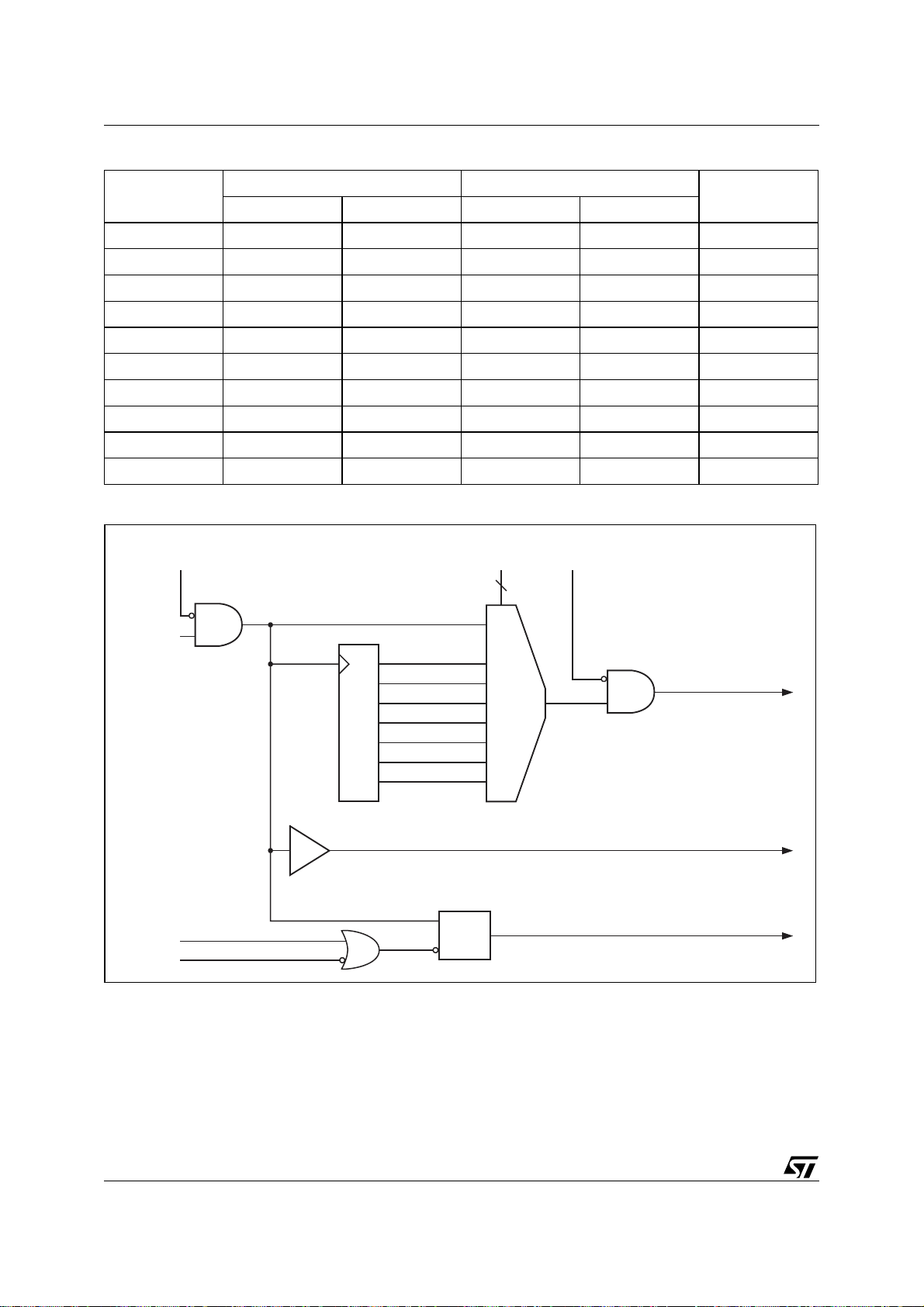
uPSD34xx - MCU CLOCK GENERATION
Table 21. PLLM and PLLD Values for Different f
f
OSC
(MHz)
decimal binary decimal binary
PLLM[4:0] PLLD[3:0]
Frequencies
OSC
40.0 22 10110 8 1000 48.0
36.0 6 00110 1 0001 48.0
33.0 30 11110 9 1001 48.0
30.0 14 01110 3 0011 48.0
24.0 18 10010 3 0011 48.0
16.0 28 11100 3 0011 48.0
12.0 30 11110 2 0010 48.0
8.0 22 10110 0 0000 48.0
6.0 30 11110 0 0000 48.0
3.0 30 11110 –1 1111 48.0
Figure 14. Clock Generation Logic
PCON[1]: PD,
Power-Down Mode
XTAL1
(f
)
OSC
PCON[2:0]: CPUPS[2:0],
Clock Pre-Scaler Select
XTAL1 (default)
XTAL1 /2
Q
XTAL1 /4
Q
XTAL1 /8
Q
XTAL1 /16
Q
XTAL1 /32
Q
XTAL1 /1024
Q
XTAL1 /2048
Q
0
1
2
3
4
5
6
7
PCON[0]: IDL,
3
M
U
X
Idle Mode
MCU_CLK (f
f
USB_CLK
(MHz)
MCU
(to: 8032, WDT)
)
PCON[1]
CCON0[6]
48/264
Clock Divider
PERIPH_CLK (f
(to: TIMER0/1/2, UART0/1, PCA0/1, SPI, I2C, ADC)
CLK
PLL
EN
USB_CLK
OSC
AI10433
)
uPSD34xx - MCU CLOCK GENERATION
Table 22. CCON0: Clock Control Register (SFR F9h, reset value 50h)
Bit 7Bit 6Bit 5Bit 4Bit 3Bit 2Bit 1Bit 0
PLLM[4] PLLEN UPLLCE DBGCE CPUAR CPUPS[2:0]
Details
Bit Symbol R/W Definition
7 PLLM[4] R,W Upper bit of the 5-bit PLLM[4:0] Multiplier (Default: '0' for PLLM = 00h)
6 PLLEN R,W
5 UPLLCE R,W
PLL Enable
0 = Disable PLL operation
1 = Enable PLL operation (Default condition after reset)
USB Clock Enable
0 = USB clock is disabled (Default condition after reset)
1 = USB clock is enabled
Debug Unit Breakpoint Comparator Enable
4 DBGCE R,W
0 = JTAG Debug Unit comparators are disabled
1 = JTAG Debug Unit comparators are enabled (Default condition after
reset)
Automatic MCU Clock Recovery
3 CPUAR R,W
0 = There is no change of CPUPS[2:0] when an interrupt occurs.
1 = Contents of CPUPS[2:0] automatically become 000b whenever any
interrupt occurs.
MCUCLK Pre-Scaler
2:0 CPUPS R,W
000b: f
001b: f
010b: f
011b: f
100b: f
101b: f
110b: f
111b: f
MCU
MCU
MCU
MCU
MCU
MCU
MCU
MCU
= f
(Default after reset)
OSC
= f
/2
OSC
= f
/4
OSC
= f
/8
OSC
= f
/16
OSC
= f
/32
OSC
= f
/1024
OSC
= f
/2048
OSC
Table 23. CCON1 PLL Control Register (SFR FAh, reset value 00h)
Bit 7Bit 6Bit 5Bit 4Bit 3Bit 2Bit 1Bit 0
PLLM[3:0] PLLD[3:0]
Details
Bit Symbol R/W Definition
Lower 4 bits of the 5-bit PLLM[4:0] Multiplier (Default after reset:
7:4 PLLM[3:0] R,W
3:0 PLLD[3:0] R,W 4-bit PLL Divider (Default after reset: PLLD = 0h)
PLLM = 00h)
PLLM[4] is in the CCON0 Register.
49/264

uPSD34xx - POWER SAVING MODES
POWER SAVING MODES
The uPSD34xx is a combination of two die, or
modules, each module having its own current consumption characteristics. This section describes
reduced power modes for the MCU Module. See
the section, Power Management, page 168 for reduced power modes of the PSD Module. Total current consumption for the combined modules is
determined in the DC specifications at the end of
this document.
The MCU Module has three software-selectable
modes of reduced power operation.
■ Idle Mode
■ Power-down Mode
■ Reduced Frequency Mode
Idle Mode
Idle Mode will halt the 8032 MCU core while leaving the MCU peripherals active (Idle Mode blocks
MCU_CLK only). For lowest current consumption
in this mode, it is recommended to disable all unused peripherals, before entering Idle mode (such
as the ADC and the Debug Unit breakpoint comparators). The following functions remain fully active during Idle Mode (except if disabled by SFR
settings).
■ External Interrupts INT0 and INT1
■ Timer 0, Timer 1 and Timer 2
■ Supervisor reset from: LVD, JTAG Debug,
External RESET_IN_, but not the WTD
■ ADC
2
■ I
C Interface
■ UART0 and UART1 Interfaces
■ SPI Interface
■ Programmable Counter Array
■ USB Interface
An interrupt generated by any of these peripherals, or a reset generated from the supervisor, will
cause Idle Mode to exit and the 8032 MCU will resume normal operation.
The output state on I/O pins of MCU ports 1, 3, and
4 remain unchanged during Idle Mode.
To enter Idle Mode, the 8032 MCU executes an instruction to set the IDL bit in the SFR named
PCON, shown in Table 26., page 52. This is the
last instruction executed in normal operating mode
before Idle Mode is activated. Once in Idle Mode,
the MCU status is entirely preserved, and there
are no changes to: SP, PSW, PC, ACC, SFRs,
DATA, IDATA, or XDATA.
The following are factors related to Idle Mode exit:
– Activation of any enabled interrupt will cause
the IDL bit to be cleared by hardware,
terminating Idle Mode. The interrupt is
serviced, and following the Return from
Interrupt instruction (RETI), the next
instruction to be executed will be the one
which follows the instruction that set the IDL
bit in the PCON SFR.
– After a reset from the supervisor, the IDL bit is
cleared, Idle Mode is terminated, and the MCU
restarts after three MCU machine cycles.
Power-down Mode
Power-down Mode will halt the 8032 core and all
MCU peripherals (Power-down Mode blocks
MCU_CLK, USB_CLK, and PERIPH_CLK). This
is the lowest power state for the MCU Module.
When the PSD Module is also placed in Powerdown mode, the lowest total current consumption
for the combined die is achieved for the
uPSD34xx. See Power Management, page 168 in
the PSD Module section for details on how to also
place the PSD Module in Power-down mode. The
sequence of 8032 instructions is important when
placing both modules into Power-down Mode.
The instruction that sets the PD Bit in the SFR
named PCON (Table 26., page 52) is the last instruction executed prior to the MCU Module going
into Power-down Mode. Once in Power-down
Mode, the on-chip oscillator circuitry and all clocks
are stopped. The SFRs, DATA, IDATA,
and XDATA are preserved.
Power-down Mode is terminated only by a reset
from the supervisor, originating from the
RESET_IN_ pin, the Low-Voltage Detect circuit
(LVD), or a JTAG Debug reset command. Since
the clock to the WTD is not active during Powerdown mode, it is not possible for the supervisor to
generate a WDT reset.
Table 24., page 51 summarizes the status of I/O
pins and peripherals during Idle and Power-down
Modes on the MCU Module. Table 25., page 51
shows the state of 8032 MCU address, data, and
control signals during these modes.
Reduced Frequency Mode
The 8032 MCU consumes less current when operating at a lower clock frequency. The MCU can reduce its own clock frequency at run-time by writing
to three bits, CPUPS[2:0], in the SFR named
CCON0 described in Table 22., page 49. These
bits effectively divide the clock frequency (f
OSC
coming in from the external crystal or oscillator device. The clock division range is from 1/2 to 1/
2048, and the resulting frequency is f
MCU
.
This MCU clock division does not affect any of the
peripherals, except for the WTD. The clock driving
the WTD is the same clock driving the 8032 MCU
core as shown in Figure 14., page 48.
)
50/264
uPSD34xx - POWER SAVING MODES
MCU firmware may reduce the MCU clock frequency at run-time to consume less current when
performing tasks that are not time critical, and then
restore full clock frequency as required to perform
urgent tasks.
Returning to full clock frequency is done automatically upon an MCU interrupt, if the CPUAR Bit in
the SFR named CCON0 is set (the interrupt will
force CPUPS[2:0] = 000). This is an excellent way
til an event occurs that requires full performance.
See Table 22., page 49 for details on CPUAR.
See the DC Specifications at the end of this document to estimate current consumption based on
the MCU clock frequency.
Note: Some of the bits in the PCON SFR shown in
Table 26., page 52 are not related to power con-
trol.
to conserve power using a low frequency clock un-
Table 24. MCU Module Port and Peripheral Status during Reduced Power Modes
2
SPI, I
Mode Ports 1, 3, 4
Idle Maintain Data Active Active Active Active Active
Power-down Maintain Data Disabled Disabled Disabled Disabled Disabled Disabled
Note: 1. The Watchdog Timer is not active during Idle Mode. Other supervisor functions are active: LVD, external reset, JTAG Debug reset.
C,
UART 0,1
PCA,
TIMER
0,1,2
USB ADC EXT INT0,1
SUPERVISORY
(1)
Active
Table 25. State of 8032 MCU Bus Signals during Power-down and Idle Modes
Mode ALE PSEN_ RD_ WR_ AD0-7 A8-15
Idle0111FFhFFh
Power-down0111FFhFFh
51/264

uPSD34xx - POWER SAVING MODES
Table 26. PCON: Power Control Register (SFR 87h, reset value 00h)
Bit 7 Bit 6 Bit 5 Bit 4 Bit 3 Bit 2 Bit 1 Bit 0
SMOD0 SMOD1 – POR RCLK1 TCLK1 PD IDL
Details
Bit Symbol R/W Function
Baud Rate Double Bit (UART0)
7 SMOD0 R,W
6 SMOD1 R,W
5––Reserved
4PORR,W
3 RCLK1 R,W
2 TCLK1 R,W
1PDR,W
0IDLR,W
0 = No Doubling
1 = Doubling
(See UART Baud Rates, page 86 for details.)
Baud Rate Double Bit for 2nd UART (UART1)
0 = No Doubling
1 = Doubling
(See UART Baud Rates, page 86 for details.)
Only a power-on reset sets this bit (cold reset). Warm reset will not set
this bit.
'0,' Cleared to zero with firmware
'1,' Is set only by a power-on reset generated by Supervisory circuit (see
Power-up Reset, page 68 for details).
Received Clock Flag (UART1)
(See Table 43., page 77 for flag description.)
Transmit Clock Flag (UART1)
(See Table 43., page 77 for flag description)
Activate Power-down Mode
0 = Not in Power-down Mode
1 = Enter Power-down Mode
Activate Idle Mode
0 = Not in Idle Mode
1 = Enter Idle Mode
52/264

uPSD34xx - OSCILLATOR AND EXTERNAL COMPONENTS
OSCILLATOR AND EXTERNAL COMPONENTS
The oscillator circuit of uPSD34xx devices is a single stage, inverting amplifier in a Pierce oscillator
configuration. The internal circuitry between pins
XTAL1 and XTAL2 is basically an inverter biased
to the transfer point. Either an external quartz crystal or ceramic resonator can be used as the feedback element to complete the oscillator circuit.
Both are operated in parallel resonance. Ceramic
resonators are lower cost, but typically have a wider frequency tolerance than quartz crystals. Alternatively, an external clock source from an
oscillator or other active device may drive the
uPSD34xx oscillator circuit input directly, instead
of using a crystal or resonator.
The minimum frequency of the quartz crystal, ceramic resonator, or external clock source is 3MHz
if the USB is used. The minimum is 8MHz if I
2
C is
used. The maximum is 40MHz in all cases. This
frequency is f
, which can be divided internally
OSC
as described in MCU CLOCK
GENERATION, page 47.
The pin XTAL1 is the high gain amplifier input, and
XTAL2 is the output. To drive the uPSD34xx device externally from an oscillator or other active
device, XTAL1 is driven and XTAL2 is left opencircuit. This external source should drive a logic
low at the voltage level of 0.3 V
logic high at 0.7V V
The XTAL1 input is 5V tolerant.
Most of the quartz crystals in the range of 25MHz
to 40MHz operate in the third overtone frequency
mode. An external LC tank circuit at the XTAL2
output of the oscillator circuit is needed to achieve
the third overtone frequency, as shown in Figure
15., page 53. Without this LC circuit, the crystal
will oscillate at a fundamental frequency mode that
is about 1/3 of the desired overtone frequency.
Note: In Figure 15., page 53 crystals which are
specified to operate in fundamental mode (not
overtone mode) do not need the LC circuit components. Since quartz crystals and ceramic resonators have their own characteristics based on their
manufacturer, it is wise to also consult the manufacturer’s recommended values for external components.
or below, and
or above, up to 5.5V VCC.
CC
CC
Figure 15. Oscillator and Clock Connections
XTAL1
(in)
C1 C2
XTAL (f
Ceramic Resonator
Crystal, fundamental mode (3-40MHz)
Crystal, overtone mode (25-40MHz)
Direct Drive
XTAL
(f
OSC
OSC
)
)
XTAL1
(in)
XTAL2
(out)
Crystal or Resonator
Usage
C1 = C2
40 - 50pF
15-33pF
20pF
L1
C3 L1
None
None
10nF
XTAL2
(out)
C3
None
None
2.2µH
External Ocsillator or
Active Clock Source
No Connect
AI09198
53/264

uPSD34xx - I/O PORTS of MCU MODULE
I/O PORTS OF MCU MODULE
The MCU Module has three 8-bit I/O ports: Port 1,
Port 3, and Port 4. The PSD Module has four other
I/O ports: Port A, B, C, and D. This section describes only the I/O ports on the MCU Module.
I/O ports will function as bi-directional General
Purpose I/O (GPIO), but the port pins can have alternate functions assigned at run-time by writing to
specific SFRs. The default operating mode (during
and after reset) for all three ports is GPIO input
mode. Port pins that have no external connection
will not float because each pin has an internal
weak pull-up (~150K ohms) to V
I/O ports 3 and 4 are 5V tolerant, meaning they
can be driven/pulled externally up to 5.5V without
damage. The pins on Port 4 have a higher current
capability than the pins on Ports 1 and 3.
Three additional MCU ports (only on 80-pin
uPSD34xx devices) are dedicated to bring out the
8032 MCU address, data, and control signals to
external pins. One port, named MCUAD[7:0], has
eight multiplexed address/data bidirectional signals. The third port has MCU bus control outputs:
read, write, program fetch, and address latch.
These ports are typically used to connect external
parallel peripherals and memory devices, but they
may NOT be used as GPIO. Notice that the eight
upper address signals do not come out to pins on
the port. If high-order address signals are required
on external pins (MCU addresses A[15:8]), then
these address signals can be brought out as needed to PLD output pins or to the Address Out mode
pins on PSD Module ports. See PSD Module section, “Latched Address Output Mode, page 208 for
details.
Figure 16., page 56 represents the flexibility of pin
function routing controlled by the SFRs. Each of
the 24 pins on three ports, P1, P3, and P4, may be
individually routed on a pin-by-pin basis to a desired function.
CC
.
MCU Port Operating Modes
MCU port pins can operate as GPIO or as alternate functions (see Figure 17., page 57 through
Figure 19., page 58).
Depending on the selected pin function, a particular pin operating mode will automatically be used:
■ GPIO - Quasi-bidirectional mode
■ UART0, UART1 - Quasi-bidirectional mode
■ SPI - Quasi-bidirectional mode
■ I2C - Open drain mode
■ ADC - Analog input mode
■ PCA output - Push-Pull mode
■ PCA input - Input only (Quasi-bidirectional)
■ Timer 0,1,2 - Input only (Quasi-bidirectional)
GPIO Function. Ports in GPIO mode operate as
quasi-bidirectional pins, consistent with standard
8051 architecture. GPIO pins are individually controlled by three SFRs:
■ SFR, P1 (Table 27., page 58)
■ SFR, P3 (Table 28., page 59)
■ SFR, P4 (Table 29., page 59)
These SFRs can be accessed using the Bit Addressing mode, an efficient way to control individual port pins.
GPIO Output. Simply stated, when a logic '0' is
written to a bit in any of these port SFRs while in
GPIO mode, the corresponding port pin will enable
a low-side driver, which pulls the pin to ground,
and at the same time releases the high-side driver
and pull-ups, resulting in a logic '0' output. When a
logic '1' is written to the SFR, the low-side driver is
released, the high-side driver is enabled for just
one MCU_CLK period to rapidly make the 0-to1
transition on the pin, while weak active pull-ups
(total ~150KΩ) to V
are enabled. This structure
CC
is consistent with standard 8051 architecture. The
high side driver is momentarily enabled only for 0to-1 transitions, which is implemented with the delay function at the latch output as pictured in Fig-
ure 17., page 57, Figure 18., page 57, and Figure
19., page 58. After the high-side driver is disabled,
the two weak pull-ups remain enabled resulting in
a logic '1' output at the pin, sourcing I
uA to an
OH
external device. Optionally, an external pull-up resistor can be added if additional source current is
needed while outputting a logic '1.'
54/264

uPSD34xx - I/O PORTS of MCU MODULE
GPIO Input. To use a GPIO port pin as an input,
the low-side driver to ground must be disabled, or
else the true logic level being driven on the pin by
an external device will be masked (always reads
logic '0'). So to make a port pin “input ready”, the
corresponding bit in the SFR must have been set
to a logic '1' prior to reading that SFR bit as an input. A reset condition forces SFRs P1, P3, and P4
to FFh, thus all three ports are input ready after reset.
When a pin is used as an input, the stronger pullup “A” maintains a solid logic '1' until an external
device drives the input pin low. At this time, pull-up
“A” is automatically disabled, and only pull-up “B”
will source the external device I
uA, consistent
IH
with standard 8051 architecture.
GPIO Bi-Directional. It is possible to operate indi-
vidual port pins in bi-directional mode. For an output, firmware would simply write the
corresponding SFR bit to logic '1' or '0' as needed.
But before using the pin as an input, firmware must
first ensure that a logic '1' was the last value written to the corresponding SFR bit prior to reading
that SFR bit as an input.
GPIO Current Capability. A GPIO pin on Port 4
can sink twice as much current than a pin on either
Port 1 or Port 3 when the low-side driver is outputting a logic '0' (I
). See the DC specifications at
OL
the end of this document for full details.
Reading Port Pin vs. Reading Port Latch. When
firmware reads the GPIO ports, sometimes the actual port pin is sampled in hardware, and sometimes the port SFR latch is read and not the actual
pin, depending on the type of MCU instruction
used. These two data paths are shown in Figure
17., page 57 through Figure 19., page 58. SFR
latches are read (and not the pins) only when the
read is part of a read-modify-write instruction and
the write destination is a bit or bits in a port SFR.
These instructions are: ANL, ORL, XRL, JBC,
CPL, INC, DEC, DJNZ, MOV, CLR, and SETB. All
other types of reads to port SFRs will read the actual pin logic level and not the port latch. This is
consistent with 8051 architecture.
55/264
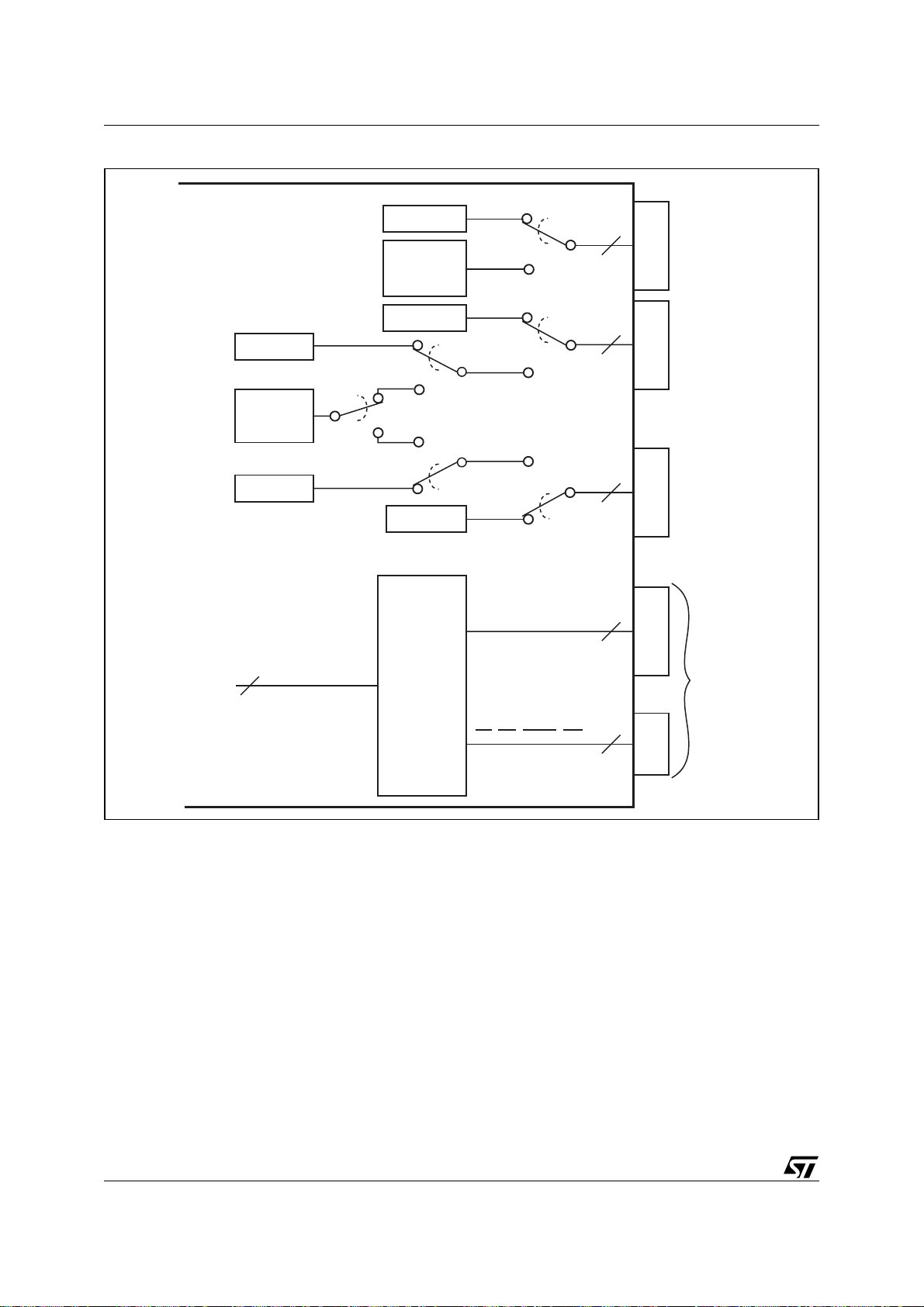
uPSD34xx - I/O PORTS of MCU MODULE
Figure 16. MCU Module Port Pin Function Routing
ADC (8)
TIMER2 (2)
UART1 (2)
SPI (4)
PCA (8)
Hi Address [15:8]
8
(Available on PSD
Module Pins)
SFR
GPIO (8)
UART0 (2)
TIMER0/1 (4)
I2C (2)
GPIO (8)
SFR
SFR
GPIO (8)
8032 MCU
CORE
MCU Module
SFR
SFR
SFR
Low Addr & Data[7:0]
RD, WR, PSEN, ALE
Ports
8
P3
8
P1
8
P4
M
C
8
U
A
D
On 80-pin
Devices
Only
C
4
N
T
L
56/264
AI09199b

Figure 17. MCU I/O Cell Block Diagram for Port 1
uPSD34xx - I/O PORTS of MCU MODULE
Select_Alternate_Func
DELAY,
1 MCU_CLK
Digital_Alt_Func_Data_Out
P1.X SFR Read Latch
(for R-M-W instructions)
SEL
Q
Q
IN 1
MUX
IN 0
DELAY,
1 MCU_CLK
Y
MCU_Reset
8032 Data Bus Bit
GPIO P1.X SFR
Write Latch
D
PRE
SFR
P1.X
Latch
P1.X SFR Read Pin
Analog_Alt_Func_En
Digital_Pin_Data_In
Analog_Pin_In
Figure 18. MCU I/O Cell Block Diagram for Port 3
Enable_I2C
Select_Alternate_Func
Digital_Alt_Func_Data_Out
P3.X SFR Read Latch
(for R-M-W instructions)
MCU_Reset
8032 Data Bus Bit
GPIO P3.X SFR
Write Latch
Disables High-Side Driver
DELAY,
1 MCU_CLK
PRE
D
SFR
Q
P3.X
Latch
Q
1 MCU_CLK
IN 1
MUX
IN 0
DELAY,
SEL
Y
V
CC
HIGH
SIDE
LOW
SIDE
V
CC
HIGH
SIDE
PULL-UP, B
PULL-UP, B
SIDE
LOW
WEAK
WEAK
V
CC
V
CC
STONGER
PULL-UP, A
P1.X Pin
AI09600
V
CC
V
CC
STONGER
PULL-UP, A
P3.X Pin
P3.X SFR Read Pin
Digital_Pin_Data_In
AI09601
57/264

uPSD34xx - I/O PORTS of MCU MODULE
Figure 19. MCU I/O Cell Block Diagram for Port 4
Enable_Push_Pull
Select_Alternate_Func
Digital_Alt_Func_Data_Out
P4.X SFR Read Latch
(for R-M-W instructions)
MCU_Reset
8032 Data Bus Bit
GPIO P4.X SFR
Write Latch
P4.X SFR Read Pin
Digital_Pin_Data_In
For PCA Alternate Function
DELAY,
1 MCU_CLK
IN 1
PRE
D
SFR
P4.X
Latch
Q
Q
IN 0
1 MCU_CLK
MUX
DELAY,
SEL
V
CC
STONGER
PULL-UP, A
P4.X Pin
AI09602
WEAK
PULL-UP, B
V
CC
V
CC
HIGH
SIDE
Y
LOW
SIDE
Table 27. P1: I/O Port 1 Register (SFR 90h, reset value FFh)
Bit 7Bit 6Bit 5Bit 4Bit 3Bit 2Bit 1Bit 0
P1.7 P1.6 P1.5 P1.4 P1.3 P1.2 P1.1 P1.0
Details
Bit Symbol R/W
Function
7 P1.7 R,W Port pin 1.7
6 P1.6 R,W Port pin 1.6
5 P1.5 R,W Port pin 1.5
4 P1.4 R,W Port pin 1.4
3 P1.3 R,W Port pin 1.3
2 P1.2 R,W Port pin 1.2
1 P1.1 R,W Port pin 1.1
0 P1.0 R,W Port pin 1.0
Note: 1. Write '1' or '0' for pin output. Read for pin input, but prior to READ, this bit must have been set to '1' by firmware or by a reset event.
(1)
58/264

uPSD34xx - I/O PORTS of MCU MODULE
Table 28. P3: I/O Port 3 Register (SFR B0h, reset value FFh)
Bit 7Bit 6Bit 5Bit 4Bit 3Bit 2Bit 1Bit 0
P3.7 P3.6 P3.5 P3.4 P3.3 P3.2 P3.1 P3.0
Details
Bit Symbol R/W
Function
7 P3.7 R,W Port pin 3.7
6 P3.6 R,W Port pin 3.6
5 P3.5 R,W Port pin 3.5
4 P3.4 R,W Port pin 3.4
3 P3.3 R,W Port pin 3.3
2 P3.2 R,W Port pin 3.2
1 P3.1 R,W Port pin 3.1
0 P3.0 R,W Port pin 3.0
Note: 1. Write '1' or '0' for pin output. Read for pin input, but prior to READ, this bit must have been set to '1' by firmware or by a reset event.
Table 29. P4: I/O Port 4 Register (SFR C0h, reset value FFh)
Bit 7Bit 6Bit 5Bit 4Bit 3Bit 2Bit 1Bit 0
P4.7 P4.6 P4.5 P4.4 P4.3 P4.2 P4.1 P4.0
Details
Bit Symbol R/W
7 P4.7 R,W Port pin 4.7
6 P4.6 R,W Port pin 4.6
5 P4.5 R,W Port pin 4.5
4 P4.4 R,W Port pin 4.4
3 P4.3 R,W Port pin 4.3
2 P4.2 R,W Port pin 4.2
1 P4.1 R,W Port pin 4.1
0 P4.0 R,W Port pin 4.0
Note: 1. Write '1' or '0' for pin output. Read for pin input, but prior to READ, this bit must have been set to '1' by firmware or by a reset event.
Function
(1)
(1)
59/264

uPSD34xx - I/O PORTS of MCU MODULE
Alternate Functions. There are five SFRs used
to control the mapping of alternate functions onto
MCU port pins, and these SFRs are depicted as
switches in Figure 16., page 56.
■ Port 3 uses the SFR, P3SFS (Table
30., page 61).
■ Port 1 uses SFRs, P1SFS0 (Table
31., page 61) and P1SFS1 (Table
32., page 61).
■ Port 4 uses SFRs, P4SFS0 (Table
34., page 62) and P4SFS1 (Table
35., page 62).
Since these SFRs are cleared by a reset, then by
default all port pins function as GPIO (not the alternate function) until firmware initializes these SFRs.
Each pin on each of the three ports can be independently assigned a different function on a pinby-pin basis.
The peripheral functions Timer 2, UART1, and I
2
may be split independently between Port 1 and
Port 4 for additional flexibility by giving a wider
choice of peripheral usage on a limited number of
device pins.
When the selected alternate function is UART0,
UART1, or SPI, then the related pins are in quasibidirectional mode, including the use of the highside driver for rapid 0-to-1 output transitions. The
high-side driver is enabled for just one MCU_CLK
period on 0-to-1 transitions by the delay function at
the “digital_alt_func_data_out” signal pictured in
Figure 17., page 57 through Figure 19., page 58.
If the alternate function is Timer 0, Timer 1, Timer
2, or PCA input, then the related pins are in quasibidirectional mode, but input only.
If the alternate function is ADC, then for each pin
the pull-ups, the high-side driver, and the low-side
driver are disabled. The analog input is routed directly to the ADC unit. Only Port 1 supports analog
functions (Figure 17., page 57). Port 1 is not 5V
tolerant.
2
If the alternate function is I
C, the related pins will
be in open drain mode, which is just like quasi-bidirectional mode but the high-side driver is not enabled for one cycle when outputting a 0-to-1
transition. Only the low-side driver and the internal
weak pull-ups are used. Only Port 3 supports
open-drain mode (Figure 18., page 57). I
quires the use of an external pull-up resistor on
each bus signal, typically 4.7KΩ to V
If the alternate function is PCA output, then the related pins are in push-pull mode, meaning the pins
are actively driven and held to logic '1' by the highside driver, or actively driven and held to logic '0'
by the low-side driver. Only Port 4 supports pushpull mode (Figure 19., page 58). Port 4 push-pull
pins can source I
C
and sink I
current when driving logic '0.' This
OL
current when driving logic '1,'
OH
current is significantly more than the capability of
pins on Port 1 or Port 3 (see Table
156., page 238).
For example, to assign these port functions:
■ Port 1: UART1, ADC[1:0], P1[7:4] are GPIO
■ Port 3: UART0, I
■ Port 4: TCM0, SPI, P4[3:1] are GPIO
2
C, P3[5:2] are GPIO
The following values need to be written to the
SFRs:
P1SFS0 = 00001111b, or 0Fh
P1SFS1 = 00000011b , or 03h
P3SFS = 11000011b, or C3h
P4SFS0 = 11110001b, or F1h
P4SFS1 = 11110000b, or F0h
CC
2
C re-
.
60/264

uPSD34xx - I/O PORTS of MCU MODULE
Table 30. P3SFS: Port 3 Special Function Select Register (SFR 91h, reset value 00h)
Bit 7Bit 6Bit 5Bit 4Bit 3Bit 2Bit 1Bit 0
P3SFS7 P3SFS6 P3SFS5 P3SFS4 P3SFS3 P3SFS2 P3SFS1 P3SFS0
Details
Port 3 Pin R/W
0 R,W GPIO UART0 Receive, RXD0
1 R,W GPIO UART0 Transmit, TXD0
2 R,W GPIO Ext Intr 0/Timer 0 Gate, EXT0INT/TG0
3 R,W GPIO Ext Intr 1/Timer 1 Gate, EXT1INT/TG1
4 R,W GPIO Counter 0 Input, C0
5 R,W GPIO Counter 0 Input, C1
6R,W GPIO
7R,W GPIO
Table 31. P1SFS0: Port 1 Special Function Select 0 Register (SFR 8Eh, reset value 00h)
Bit 7Bit 6Bit 5Bit 4Bit 3Bit 2Bit 1Bit 0
P1SF07 P1SF06 P1SF05 P1SF04 P1SF03 P1SF02 P1SF01 P1SF00
Details
Default Port Function Alternate Port Function
P3SFS[i] - 0; Port 3 Pin, i = 0..7 P3SFS[i] - 1; Port 3 Pin, i = 0..7
2
I
C Data, I2CSDA
2
C Clock, I2CCL
I
Table 32. P1SFS1: Port 1 Special Function Select 1 Register (SFR 8Fh, reset value 00h)
Bit 7Bit 6Bit 5Bit 4Bit 3Bit 2Bit 1Bit 0
P1SF17 P1SF16 P1SF15 P1SF14 P1SF13 P1SF12 P1SF11 P1SF10
Table 33. P1SFS0 and P1SFS1 Details
Default Port Function Alternate 1 Port Function Alternate 2 Port Function
Port 1 Pin R/W
0 R,W GPIO Timer 2 Count Input, T2 ADC Chn 0 Input, ADC0
1 R,W GPIO Timer 2 Trigger Input, TX2 ADC Chn 1 Input, ADC1
2 R,W GPIO UART1 Receive, RXD1 ADC Chn 2 Input, ADC2
3 R,W GPIO UART1 Transmit, TXD1 ADC Chn 3 Input, ADC3
4 R,W GPIO SPI Clock, SPICLK ADC Chn 4 Input, ADC4
5 R,W GPIO SPI Receive, SPIRXD ADC Chn 5 Input, ADC5
6 R,W GPIO SPI Transmit, SPITXD ADC Chn 6 Input, ADC6
7 R,W GPIO SPI Select, SPISEL_ ADC Chn 7 Input, ADC7
P1SFS0[i] = 0
P1SFS1[i] = x
Port 1 Pin, i = 0.. 7 Port 1 Pin, i = 0.. 7 Port 1 Pin, i = 0.. 7
P1SFS0[i] = 1
P1SFS1[i] = 0
P1SFS0[i] = 1
P1SFS1[i] = 1
61/264

uPSD34xx - I/O PORTS of MCU MODULE
Table 34. P4SFS0: Port 4 Special Function Select 0 Register (SFR 92h, reset value 00h)
Bit 7Bit 6Bit 5Bit 4Bit 3Bit 2Bit 1Bit 0
P4SF07 P4SF06 P4SF05 P4SF04 P4SF03 P4SF02 P4SF01 P4SF00
Details
Table 35. P4SFS1: Port 4 Special Function Select 1 Register (SFR 93h, reset value 00h)
Bit 7Bit 6Bit 5Bit 4Bit 3Bit 2Bit 1Bit 0
P4SF17 P4SF16 P4SF15 P4SF14 P4SF13 P4SF12 P4SF11 P4SF10
Table 36. P4SFS0 and P4SFS1 Details
Default Port Function Alternate 1 Port Function Alternate 2 Port Function
Port 4 Pin R/W
0 R,W GPIO PCA0 Module 0, TCM0 Timer 2 Count Input, T2
1 R,W GPIO PCA0 Module 1, TCM1 Timer 2 Trigger Input, TX2
2 R,W GPIO PCA0 Module 2, TCM2 UART1 Receive, RXD1
3 R,W GPIO PCA0 Ext Clock, PCACLK0 UART1 Transmit, TXD1
4 R,W GPIO PCA1 Module 3, TCM3 SPI Clock, SPICLK
5 R,W GPIO PCA1 Module 4, TCM4 SPI Receive, SPIRXD
6 R,W GPIO PCA1 Module 5, TCM5 SPI Transmit, SPITXD
7 R,W GPIO PCA1 Ext Clock, PCACLK1 SPI Select, SPISEL_
P4SFS0[i] = 0
P4SFS1[i] = x
Port 4 Pin, i = 0.. 7 Port 4 Pin, i = 0.. 7 Port 4 Pin, i = 0.. 7
P4SFS0[i] = 1
P4SFS1[i] = 0
P4SFS0[i] = 1
P4SFS1[i] = 1
62/264

MCU BUS INTERFACE
The MCU Module has a programmable bus interface which is a modified 8032 bus with 16 multiplexed address and data lines. The bus supports
four types of data transfer (16- or 8-bit), each
transfer is to/from a memory location external to
the MCU Module:
– Code Fetch cycle using the PSEN signal: fetch
a 16-bit code word for filling the pre-fetch
queue. The CPU fetches a code byte from the
PFQ for execution;
– Code Read cycle using PSEN: read a 16-bit
code word using the MOVC (Move Constant)
instruction. The code word is routed directly to
the CPU and by-pass the PFQ;
– XDATA Read cycle using the RD signal: read
a data byte using the MOVX (Move eXternal)
instruction; and
– XDATA Write cycle using the WR signal: write
a data byte using the MOVX instruction
PSEN Bus Cycles
In a PSEN bus cycle, the MCU module fetches the
instruction from the 16-bit program memory in the
PSD module. The multiplexed address/data bus
AD[15:0] is connected to the PSD module for 16bit data transfer. The uPSD34xx does not support
external PSEN cycles and cannot fetch instruction
from other external program memory devices.
READ or WRITE Bus Cycles
In an XDATA READ or WRITE bus cycle, the
MCU’s multiplexed AD[15:0] bus is connected to
the PSD module, but only the lower bytes AD[7:0]
are used for the 8-bit data transfer. The AD[7:0]
lines are also connected to pins in the 80-pin pack-
uPSD34xx - MCU BUS INTERFACE
age for accessing external devices. If the high address byte A[15:8] is needed for external devices,
Port B in the PSD Module can be configured to
provide the latched A[15:8] address outputs.
Connecting External Devices to the MCU Bus
The uPSD34xx supports 8-bit only external I/O or
Data memory devices. The READ and WRITE
data transfer is carried out on the AD[7:0] bus
which is available in the 80-pin package. The address lines can be brought out to the external devices in one of three ways:
1. Configure Ports B and A of the PSD Module in
Address Output mode, as shown in Figure 20;
2. Use Port B together with an external latch, as
shown in Figure 21., page 64. The external
latch latches the low address byte from the
AD[7:0] bus with the ALE signal.This
configuration is for design where Port A is
needed for CPLD functions; and
3. Configure the microcell in the CPLD to output
any address line to any of the CPLD output
pins. This is the most flexible implementation
but requires the use of CPLD resources.
Ports A and B in the PSD Module can be configured in the PSDsoft to provide latched MCU address A[7:0] and A[15:8] (see PSD Module
Detailed Operation, page 178 for details on how to
enable Address Output mode). The latched address outputs on the ports are pin configurable.
For example, Port B pins PB[2:0] can be enabled
to provide A[10:8] and the remaining pins can be
configured for other functions such as generating
chip selects to the external devices.
Figure 20. Connecting External Devices using Ports A and B for Address AD[15:0]
uPSD34xx
Module
AI10434
MCU
AD[7:0]
AD[15:8]
PSEN
ALE
RD or WR
PSD
Module
D[7:0]
RD or WR
Por t B
Por t A
A8-15
A0-7
CS
External
8-bit
Device
63/264
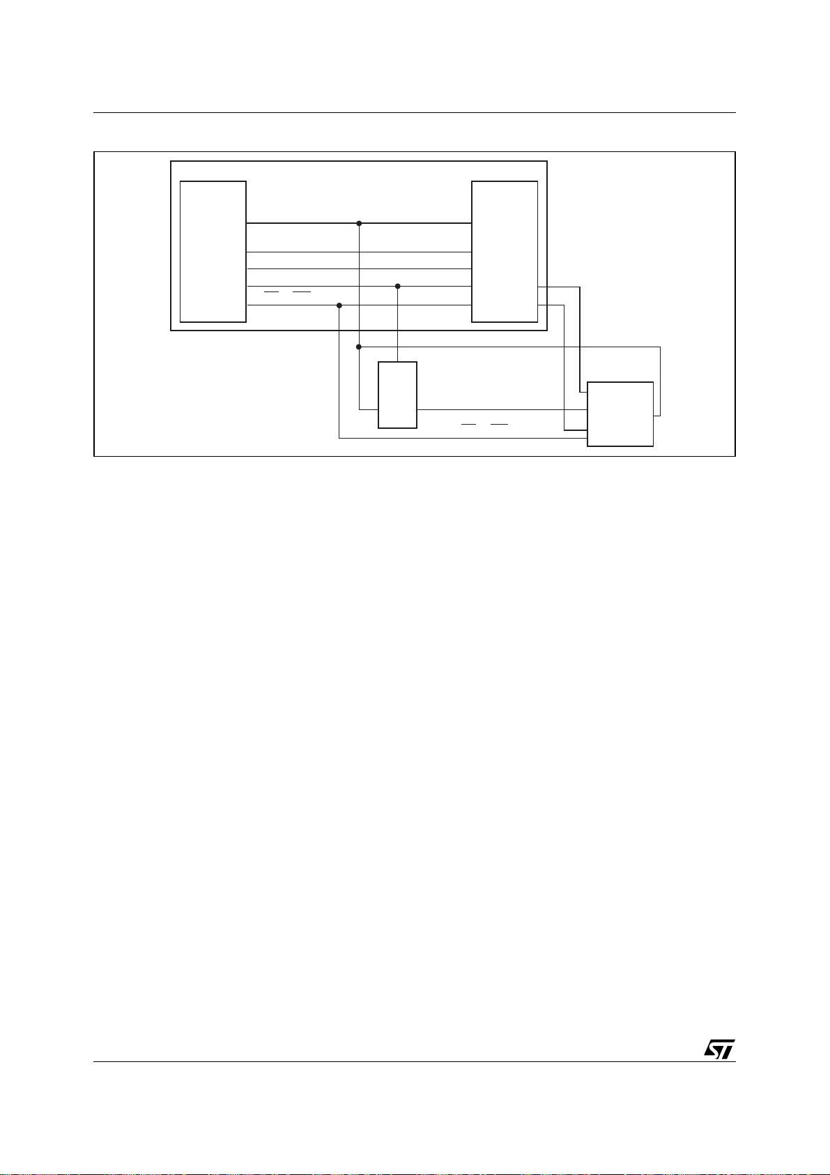
uPSD34xx - MCU BUS INTERFACE
Figure 21. Connecting External Devices using Port A and an External Latch for Address AD[15:0]
uPSD34xx
MCU
Module
AI10435
AD[7:0]
AD[15:8]
PSEN
ALE
RD or WR
Programmable Bus Timing
The length of the bus cycles are user programmable at run time. The number of MCU_CLK periods
in a bus cycle can be specified in the SFR register
named BUSCON (see Table 37., page 65). By default, the BUSCON Register is loaded with long
bus cycle times (6 MCU_CLK periods) after a reset condition. It is important that the post-reset initialization firmware sets the bus cycle times
appropriately to get the most performance, according to Table 38., page 66. Keep in mind that
the PSD Module has a faster Turbo Mode (default)
and a slower but less power consuming Non-Turbo Mode. The bus cycle times must be programmed in BUSCON to optimize for each mode
as shown in Table 38. See PSD Module Detailed
Operation, page 178 for more details.
It is not possible to specify in the BUSCON Register a different number of MCU_CLK periods for
various address ranges. For example, the user
cannot specify 4 MCU_CLK periods for RD read
cycles to one address range on the PSD Module,
and 5 MCU_CLK periods for RD read cycles to a
different address range on an external device.
However, the user can specify one number of
clock periods for PSEN read cycles and a different
number of clock periods for RD or WR cycles (see
Figure Figure 22., page 65).
PSD
Module
Por t B
D[7:0]
L
A
T
C
H
A7-0
RD or WR
A8-15
CS
External
8-bit
Device
Controlling the PFQ and BC
The BUSCON Register allows firmware to enable
and disable the PFQ and BC at run-time. Sometimes it may be desired to disable the PFQ and BC
to ensure deterministic execution. The dynamic
action of the PFQ and BC may cause varying program execution times depending on the events
that happen prior to a particular section of code of
interest. For this reason, it is not recommended to
implement timing loops in firmware, but instead
use one of the many hardware timers in the
uPSD34xx. By default, the PFQ and BC are enabled after a reset condition.
Important: Disabling the PFQ or BC will seriously
reduce MCU performance.
64/264

Figure 22. A RD or PSEN Bus Cycle Set to 5 MCU_CLK
1
MCU Clock
ALE
2
uPSD34xx - MCU BUS INTERFACE
3
4
5
AD0-AD15
RD/PSEN
Note: 1. The PSEN cycle is 16-bit, while the RD cycle is 8-bit only.
2. A PSEN bus cycle in progress may be aborted before completion if the PFQ and Branch Cache (BC) determines the current code
fetch cycle is not needed.
3. Whenever the same number of MCU_CLK periods is specified in BUSCON for both PSEN and RD cycles, the bus cycle timing is
typically identical for each of these types of bus cycles. In this case, the only time PSEN read cycles are longer than RD read cycles
is when the PFQ issues a stall while reloading. PFQ stalls do not affect RD read cycles. By comparison, in many traditional 8051
architectures, RD bus cycles are always longer than PSEN bus cycles.
(2,3)
A0-A15
5-Clock Bus Cycle
D0-D15
(1)
AI10436
Table 37. BUSCON: Bus Control Register (SFR 9Dh, reset value EBh)
Bit 7Bit 6Bit 5Bit 4Bit 3Bit 2Bit 1Bit 0
EPFQ EBC WRW[1:0] RDW[1:0] CW[1:0]
Details
Bit Symbol R/W Definition
Enable Pre-Fetch Queue
7 EPFQ R,W
6 EBC R,W
5:4 WRW[1:0] R,W
3:2 RDW[1:0] R,W
1:0 CW[1:0] R,W
0 = PFQ is disabled
1 = PFQ is enabled (default)
Enable Branch Cache
0 = BC is disabled
1 = BC is enabled (default)
WR
Wait, number of MCU_CLK periods for WR write bus cycle during
any MOVX instruction
00b: 4 clock periods
01b: 5 clock periods
10b: 6 clock periods (default)
11b: 7 clock periods
RD
Wait, number of MCU_CLK periods for RD read bus cycle during any
MOVX instruction
00b: 4 clock periods
01b: 5 clock periods
10b: 6 clock periods (default)
11b: 7 clock periods
Code Wait, number of MCU_CLK periods for PSEN
read bus cycle
during any code byte fetch or during any MOVC code byte read
instruction. Periods will increase with PFQ stall
00b: 3 clock periods - exception, for MOVC instructions this setting
results 4 clock periods
01b: 4 clock periods
10b: 5 clock periods
11b: 6 clock periods (default)
65/264
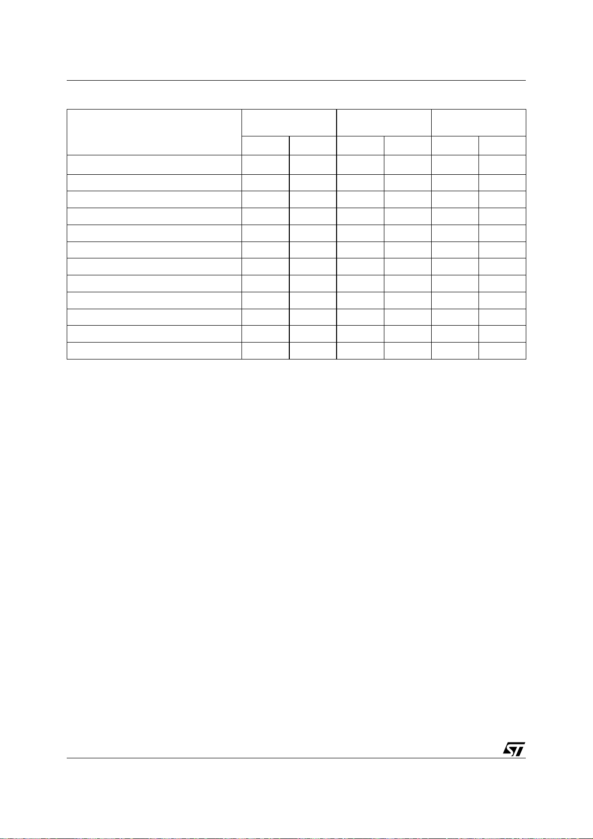
uPSD34xx - MCU BUS INTERFACE
Table 38. Number of MCU_CLK Periods Required to Optimize Bus Transfer Rate
MCU Clock Frequency,
MCU_CLK (f
40MHz, Turbo mode PSD
MCU
(2)
CW[1:0] Clk Periods
)
3.3V
(1)
5V
(1)
545454
RDW[1:0] Clk
Periods
(1)
3.3V
5V
(1)
40MHz, Non-Turbo mode PSD 656565
36MHz, Turbo mode PSD 545454
36MHz, Non-Turbo mode PSD 646464
32MHz, Turbo mode PSD 545454
32MHz, Non-Turbo mode PSD 545454
28MHz, Turbo mode PSD 434444
28MHz, Non-Turbo mode PSD 545454
24MHz, Turbo mode PSD 434444
24MHz, Non-Turbo mode PSD 434444
20MHz and below, Turbo mode PSD 334444
20MHz and below, Non-Turbo mode PSD 334444
Note: 1. VDD of the PSD Module
2. “Turbo mode PSD” means that the PSD Module is in the faster, Turbo mode (default condition). A PSD Module in Non-Turbo mode
is slower, but consumes less current. See PSD Module section, titled “PLD Non-Turbo Mode” for details.
WRW[1:0] Clk
Periods
(1)
3.3V
5V
(1)
66/264
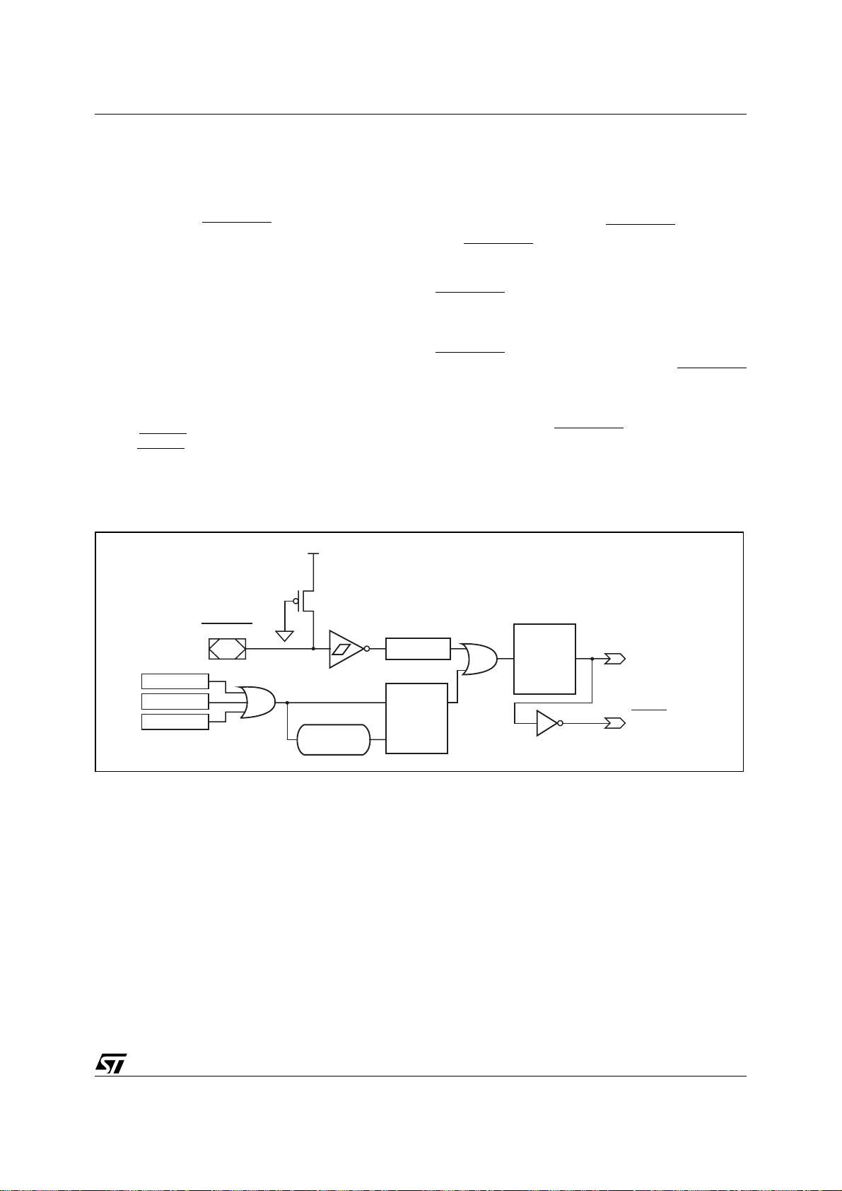
SUPERVISORY FUNCTIONS
Supervisory circuitry on the MCU Module will issue
an internal reset signal to the MCU Module and simultaneously to the PSD Module as a result of any
of the following four events:
– The external RESET_IN
– The Low Voltage Detect (LVD) circuitry has
detected a voltage on V
threshold (power-on or voltage sags)
– The JTAG Debug interface has issued a reset
command
– The Watch Dog Timer (WDT) has timed out
The resulting internal reset signal, MCU_RESET,
will force the 8032 into a known reset state while
asserted, and then 8032 program execution will
jump to the reset vector at program address 0000h
just after MCU_RESET is deasserted. The MCU
Module will also assert an active low internal reset
signal, RESET
signal RESET
, to the PSD Module. If needed, the
can be driven out to external system components through any PLD output pin on
the PSD Module. When driving this
pin is asserted
below a specific
CC
uPSD34xx - SUPERVISORY FUNCTIONS
“RESET_OUT” signal from a PLD output, the user
can choose to make it either active-high or activelow logic, depending on the PLD equation.
External Reset Input Pin, RESET_IN
The RESET_IN pin can be connected directly to a
mechanical reset switch or other device which
pulls the signal to ground to invoke a reset.
RESET_IN
Schmitt trigger input buffer with a voltage hysteresis of V
signal rise and fall times, as shown in Figure 23.
RESET_IN
less than a duration of t
signal must be maintained at a logic '0' for at least
a duration of t
ning. The resulting MCU_RESET signal will last
only as long as the RESET_IN
not stretched). Refer to the Supervisor AC specifications in Table 178., page 253 at the end of this
document for these parameter values.
is pulled up internally and enters a
RST_HYS
for immunity to the effects of slow
is also filtered to reject a voltage spike
. The RESET_IN
RST_LO_IN
RST_FIL
while the oscillator is run-
signal is active (it is
Figure 23. Supervisor Reset Generation
V
CC
PULL-UP
RESET_IN
PIN
WDT
LV D
JTAG Debug
DELAY,
t
RST_ACTV
Noise Filter
S
R
MCU
Clock
Sync
Q
MCU_RESET
to MCU and
Peripherals
RESET
to PSD Module
AI09603
67/264

uPSD34xx - SUPERVISORY FUNCTIONS
Low VCC Voltage Detect, LVD
An internal reset is generated by the LVD circuit
when V
V
LV_THRESH
old, the MCU_RESET signal will remain asserted
for t
RST_ACTV
is always enabled (cannot be disabled by SFR),
even in Idle Mode and Power-down Mode. The
LVD input has a voltage hysteresis of V
and will reject voltage spikes less than a duration
of t
RST_FIL
Important: The LVD voltage threshold is
V
LV_THRESH
supply on the MCU Module and the 3.3V V
V
CC
supply on the PSD Module for 3.3V uPSD34xxV
devices, since these supplies are one in the same
on the circuit board.
However, for 5V uPSD34xx devices, V
is not suitable for monitoring the 5V VDD voltage
supply (V
itoring the 3.3V V
uPSD34xx devices, an external means is required
to monitor the separate 5V V
Power-up Reset
At power up, the internal reset generated by the
LVD circuit is latched as a logic '1' in the POR bit
of the SFR named PCON (Table 26., page 52).
Software can read this bit to determine whether
the last MCU reset was the result of a power up
(cold reset) or a reset from some other condition
(warm reset). This bit must be cleared with software.
JTAG Debug Reset
The JTAG Debug Unit can generate a reset for debugging purposes. This reset source is also available when the MCU is in Idle Mode and PowerDown Mode (the user can use the JTAG debugger
to exit these modes).
Watchdog Timer, WDT
When enabled, the WDT will generate a reset
whenever it overflows. Firmware that is behaving
correctly will periodically clear the WDT before it
overflows. Run-away firmware will not be able to
clear the WDT, and a reset will be generated.
drops below the reset threshold,
CC
. After VCC returns to the reset thresh-
before it is released. The LVD circuit
RST_HYS
.
, suitable for monitoring both the 3.3V
LV_THRESH
LV_THRESH
is too low), but good for mon-
supply. In the case of 5V
CC
supply, if desired.
DD
DD
By default, the WDT is disabled after each reset.
Note: The WDT is not active during Idle mode or
Power-down Mode.
There are two SFRs that control the WDT, they are
WDKEY (Table 39., page 70) and WDRST (Table
40., page 70).
If WDKEY contains 55h, the WDT is disabled. Any
value other than 55h in WDKEY will enable the
WDT. By default, after any reset condition, WDKEY is automatically loaded with 55h, disabling
the WDT. It is the responsibility of initialization
firmware to write some value other than 55h to
WDKEY after each reset if the WDT is to be used.
The WDT consists of a 24-bit up-counter (Figure
24), whose initial count is 000000h by default after
every reset. The most significant byte of this
counter is controlled by the SFR, WDRST. After
being enabled by WDKEY, the 24-bit count is increased by 1 for each MCU machine cycle. When
the count overflows beyond FFFFFh (2
24
MCU
machine cycles), a reset is issued and the WDT is
automatically disabled (WDKEY = 55h again).
To prevent the WDT from timing out and generating a reset, firmware must repeatedly write some
value to WDRST before the count reaches
FFFFFh. Whenever WDRST is written, the upper
8 bits of the 24-bit counter are loaded with the written value, and the lower 16 bits of the counter are
cleared to 0000h.
The WDT time-out period can be adjusted by writing a value other that 00h to WDRST. For example, if WDRST is written with 04h, then the WDT
will start counting 040000h, 040001h, 040002h,
and so on for each MCU machine cycle. In this example, the WDT time-out period is shorter than if
WDRST was written with 00h, because the WDT
is an up-counter. A value for WDRST should never
be written that results in a WDT time-out period
shorter than the time required to complete the
longest code task in the application, else unwanted WDT overflows will occur.
Figure 24. Watchdog Counter
23 15 7 0
8-bits8-bits8-bits
SFR, WDRST
68/264
AI09604

uPSD34xx - SUPERVISORY FUNCTIONS
The formula to determine WDT time-out period is:
WDT
PERIOD
N
OVERFLOW
= t
MACH_CYC
x N
OVERFLOW
is the number of WDT up-counts required to reach FFFFFFh. This is determined by
the value written to the SFR, WDRST.
t
MACH_CYC
is the average duration of one MCU
machine cycle. By default, an MCU machine cycle
is always 4 MCU_CLK periods for uPSD34xx, but
the following factors can sometimes add more
MCU_CLK periods per machine cycle:
– The number of MCU_CLK periods assigned to
MCU memory bus cycles as determined in the
SFR, BUSCON. If this setting is greater than
4, then machine cycles have additional
MCU_CLK periods during memory transfers.
– Whether or not the PFQ/BC circuitry issues a
stall during a particular MCU machine cycle. A
stall adds more MCU_CLK periods to a
machine cycle until the stall is removed.
t
MACH_CYC
is also affected by the absolute time of
a single MCU_CLK period. This number is fixed by
the following factors:
– Frequency of the external crystal, resonator,
or oscillator: (f
OSC
)
– Bit settings in the SFR CCON0, which can
divide f
and change MCU_CLK
OSC
As an example, assume the following:
1. f
is 40MHz, thus its period is 25ns.
OSC
2. CCON0 is 10h, meaning no clock division, so
the period of MCU_CLK is also 25ns.
3. BUSCON is C1h, meaning the PFQ and BC
are enabled, and each MCU memory bus
cycle is 4 MCU_CLK periods, adding no
additional MCU_CLK periods to MCU
machine cycles during memory transfers.
4. Assume there are no stalls from the PFQ/BC.
In reality, there are occational stalls but their
occurance has minimal impact on WDT
timeout period.
24
5. WDRST contains 00h, meaning a full 2
upcounts are required to reach FFFFFh and
generate a reset.
In this example,
t
MACH_CYC
N
OVERFLOW
WDT
= 100ns (4 MCU_CLK periods x 25ns)
= 224 = 16777216 up-counts
PERIOD
= 100ns X 16777216 = 1.67 seconds
The actual value will be slightly longer due to PFQ/
BC.
Firmware Example: The following 8051 assembly code illustrates how to operate the WDT. A
simple statement in the reset initialization firmware
enables the WDT, and then a periodic write to
clear the WDT in the main firmware is required to
keep the WDT from overflowing. This firmware is
based on the example above (40MHz f
OSC
CCON0 = 10h, BUSCON = C1h).
For example, in the reset initialization firmware
(the function that executes after a jump to the reset
vector):
MOV AE, #AA ; enable WDT by writing value to
; WDKEY other than 55h
Somewhere in the flow of the main program, this
statement will execute periodically to reset the
WDT before its time-out period of 1.67 seconds.
For example:
MOV A6, #00 ; reset WDT, loading 000000h.
; Counting will automatically
; resume as long as 55h in not in
; WDKEY
,
69/264
uPSD34xx - SUPERVISORY FUNCTIONS
Table 39. WDKEY: Watchdog Timer Key Register (SFR AEh, reset value 55h)
Bit 7Bit 6Bit 5Bit 4Bit 3Bit 2Bit 1Bit 0
WDKEY[7:0]
Details
Bit Symbol R/W Definition
55h disables the WDT from counting. 55h is automatically loaded in this
SFR after any reset condition, leaving the WDT disabled by default.
[7:0] WDKEY W
Table 40. WDRST: Watchdog Timer Reset Counter Register (SFR A6h, reset value 00h)
Bit 7Bit 6Bit 5Bit 4Bit 3Bit 2Bit 1Bit 0
Details
Bit Symbol R/W Definition
[7:0] WDRST W
Any value other than 55h written to this SFR will enable the WDT, and
counting begins.
WDRST[7:0]
This SFR is the upper byte of the 24-bit WDT up-counter. Writing this
SFR sets the upper byte of the counter to the written value, and clears
the lower two bytes of the counter to 0000h.
Counting begins when WDKEY does not contain 55h.
70/264

uPSD34xx - STANDARD 8032 TIMER/COUNTERS
STANDARD 8032 TIMER/COUNTERS
There are three 8032-style 16-bit Timer/Counter
registers (Timer 0, Timer 1, Timer 2) that can be
configured to operate as timers or event counters.
There are two additional 16-bit Timer/Counters in
the Programmable Counter Array (PCA), seePCA
Block, page 154 for details.
Standard Timer SFRs
Timer 0 and Timer 1 have very similar functions,
and they share two SFRs for control:
■ TCON (Table 41., page 72)
■ TMOD (Table 42., page 74).
Timer 0 has two SFRs that form the 16-bit counter,
or that can hold reload values, or that can scale
the clock depending on the timer/counter mode:
■ TH0 is the high byte, address 8Ch
■ TL0 is the low byte, address 8Ah
Timer 1 has two similar SFRs:
■ TH1 is the high byte, address 8Dh
■ TL1 is the low byte, address 8Bh
Timer 2 has one control SFR:
■ T2CON (Table 43., page 77)
Timer 2 has two SFRs that form the 16-bit counter,
and perform other functions:
■ TH2 is the high byte, address CDh
■ TL2 is the low byte, address CCh
Timer 2 has two SFRs for capture and reload:
■ RCAP2H is the high byte, address CBh
■ RCAP2L is the low byte, address CAh
Clock Sources
When enabled in the “Timer” function, the Registers THx and TLx are incremented every 1/12 of
the oscillator frequency (f
). This timer clock
OSC
source is not effected by MCU clock dividers in the
CCON0, stalls from PFQ/BC, or bus transfer cycles. Timers are always clocked at 1/12 of f
OSC
.
When enabled in the “Counter” function, the Registers THx and TLx are incremented in response to
a 1-to-0 transition sampled at their corresponding
external input pin: pin C0 for Timer 0; pin C1 for
Timer 1; or pin T2 for Timer 2. In this function, the
external clock input pin is sampled by the counter
at a rate of 1/12 of f
. When a logic '1' is deter-
OSC
mined in one sample, and a logic '0' in the next
sample period, the count is incremented at the
very next sample period (period1: sample=1,
period2: sample=0, period3: increment count
while continuing to sample). This means the maximum count rate is 1/24 of the f
. There are no
OSC
restrictions on the duty cycle of the external input
signal, but to ensure that a given level is sampled
at least once before it changes, it should be active
for at least one full sample period (12 / f
OSC,
seconds). However, if MCU_CLK is divided by the
SFR CCON0, then the sample period must be calculated based on the resultant, longer, MCU_CLK
frequency. In this case, an external clock signal on
pins C0, C1, or T2 should have a duration longer
than one MCU machine cycle, t
MACH_CYC
. The
section, Watchdog Timer, WDT, page 68 explains
how to estimate t
MACH_CYC
.
71/264
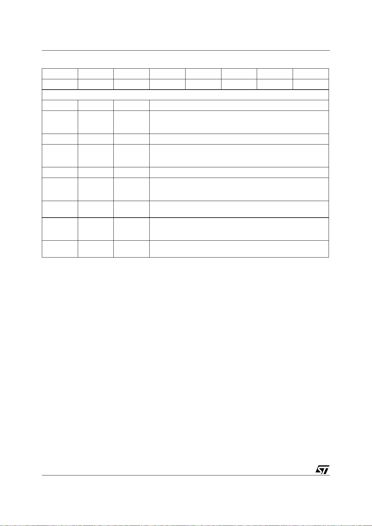
uPSD34xx - STANDARD 8032 TIMER/COUNTERS
Table 41. TCON: Timer Control Register (SFR 88h, reset value 00h)
Bit 7Bit 6Bit 5Bit 4Bit 3Bit 2Bit 1Bit 0
TF1 TR1 TF0 TR0 IE1 IT1 IE0 IT0
Details
Bit Symbol R/W Definition
Timer 1 overflow interrupt flag. Set by hardware upon overflow.
7 TF1 R
6 TR1 R,W Timer 1 run control. 1 = Timer/Counter 1 is on, 0 = Timer/Counter 1 is off.
5 TF0 R
4 TR0 R,W Timer 0 run control. 1 = Timer/Counter 0 is on, 0 = Timer/Counter 0 is off.
3IE1R
2IT1R,W
1IE0R
0IT0R,W
Automatically cleared by hardware after firmware services the interrupt
for Timer 1.
Timer 0 overflow interrupt flag. Set by hardware upon overflow.
Automatically cleared by hardware after firmware services the interrupt
for Timer 0.
Interrupt flag for external interrupt pin, EXTINT1. Set by hardware when
edge is detected on pin. Automatically cleared by hardware after
firmware services EXTINT1 interrupt.
Trigger type for external interrupt pin EXTINT1. 1 = falling edge, 0 = lowlevel
Interrupt flag for external interrupt pin, EXTINT0. Set by hardware when
edge is detected on pin. Automatically cleared by hardware after
firmware services EXTINT0 interrupt.
Trigger type for external interrupt pin EXTINT0. 1 = falling edge, 0 = lowlevel
72/264

uPSD34xx - STANDARD 8032 TIMER/COUNTERS
SFR, TCON
Timer 0 and Timer 1 share the SFR, TCON, that
controls these timers and provides information
about them. See Table 41., page 72.
Bits IE0 and IE1 are not related to Timer/Counter
functions, but they are set by hardware when a
signal is active on one of the two external interrupt
pins, EXTINT0 and EXTINT1. For system information on all of these interrupts, see Table
16., page 42, Interrupt Summary.
Bits IT0 and IT1 are not related to Timer/Counter
functions, but they control whether or not the two
external interrupt input pins, EXTINT0 and
EXTINT1 are edge or level triggered.
SFR, TMOD
Timer 0 and Timer 1 have four modes of operation
controlled by the SFR named TMOD (Table 42).
Timer 0 and Timer 1 Operating Modes
The “Timer” or “Counter” function is selected by
the C/T
modes are selected by bit-pairs M[1:0] in TMOD.
Modes 0, 1, and 2 are the same for both Timer/
Counters. Mode 3 is different.
Mode 0. Putting either Timer/Counter into Mode 0
makes it an 8-bit Counter with a divide-by-32 prescaler. Figure 25 shows Mode 0 operation as it applies to Timer 1 (same applies to Timer 0).
In this mode, the Timer Register is configured as a
13-bit register. As the count rolls over from all '1s'
to all '0s,' it sets the Timer Interrupt flag TF1. The
counted input is enabled to the Timer when
TR1 = 1 and either GATE = 0 or EXTINT1 = 1.
(Setting GATE = 1 allows the Timer to be controlled by external input pin, EXTINT1, to facilitate
pulse width measurements). TR1 is a control bit in
the SFR, TCON. GATE is a bit in the SFR, TMOD.
The 13-bit register consists of all 8 bits of TH1 and
the lower 5 bits of TL1. The upper 3 bits of TL1 are
indeterminate and should be ignored. Setting the
run flag, TR1, does not clear the registers.
control bits in TMOD. The four operating
Mode 0 operation is the same for the Timer 0 as
for Timer 1. Substitute TR0, TF0, C0, TL0, TH0,
and EXTINT0 for the corresponding Timer 1 signals in Figure 25. There are two different GATE
Bits, one for Timer 1 and one for Timer 0.
Mode 1. Mode 1 is the same as Mode 0, except
that the Timer Register is being run with all 16 bits.
Mode 2. Mode 2 configures the Timer Register as
an 8-bit Counter (TL1) with automatic reload, as
shown in Figure 26., page 75. Overflow from TL1
not only sets TF1, but also reloads TL1 with the
contents of TH1, which is preset with firmware.
The reload leaves TH1 unchanged. Mode 2 operation is the same for Timer/Counter 0.
Mode 3. Timer 1 in Mode 3 simply holds its count.
The effect is the same as setting TR1 = 0.
Timer 0 in Mode 3 establishes TL0 and TH0 as two
separate counters. The logic for Mode 3 on Timer
0 is shown in Figure 27., page 75. TL0 uses the
Timer 0 control Bits: C/T
, GATE, TR0, and TF0, as
well as the pin EXTINT0. TH0 is locked into a timer
function (counting at a rate of 1/12 f
) and takes
OSC
over the use of TR1 and TF1 from Timer 1. Thus,
TH0 now controls the “Timer 1“ interrupt flag.
Mode 3 is provided for applications requiring an
extra 8-bit timer on the counter (see Figure
27., page 75). With Timer 0 in Mode 3, a
uPSD34xx device can look like it has three Timer/
Counters (not including the PCA). When Timer 0 is
in Mode 3, Timer 1 can be turned on and off by
switching it out of and into its own Mode 3, or can
still be used by the serial port as a baud rate generator, or in fact, in any application not requiring an
interrupt.
73/264

uPSD34xx - STANDARD 8032 TIMER/COUNTERS
Table 42. TMOD: Timer Mode Register (SFR 89h, reset value 00h)
Bit 7Bit 6Bit 5Bit 4Bit 3Bit 2Bit 1Bit 0
GATE C/T
Details
Bit Symbol R/W Timer Definition (T/C is abbreviation for Timer/Counter)
M[1:0] GATE C/T M[1:0]
Gate control.
7GATER,W
6C/T
[5:4] M[1:0] R,W
3GATER,W
2C/T
R,W
R,W
Timer 1
Timer 0
When GATE = 1, T/C is enabled only while pin EXTINT1
is '1' and the flag TR1 is '1.' When GATE = 0, T/C is
enabled whenever the flag TR1 is '1.'
Counter or Timer function select.
When C/T = 0, function is timer, clocked by internal clock.
C/T
= 1, function is counter, clocked by signal sampled on
external pin, C1.
Mode Select.
00b = 13-bit T/C. 8 bits in TH1 with TL1 as 5-bit prescaler.
01b = 16-bit T/C. TH1 and TL1 are cascaded. No prescaler.
10b = 8-bit auto-reload T/C. TH1 holds a constant and
loads into TL1 upon overflow.
11b = Timer Counter 1 is stopped.
Gate control.
When GATE = 1, T/C is enabled only while pin EXTINT0
is '1' and the flag TR0 is '1.' When GATE = 0, T/C is
enabled whenever the flag TR0 is '1.'
Counter or Timer function select.
When C/T = 0, function is timer, clocked by internal clock.
C/T
= 1, function is counter, clocked by signal sampled on
external pin, C0.
Mode Select.
[1:0] M[1:0] R,W
74/264
00b = 13-bit T/C. 8 bits in TH0 with TL0 as 5-bit prescaler.
01b = 16-bit T/C. TH0 and TL0 are cascaded. No prescaler.
10b = 8-bit auto-reload T/C. TH0 holds a constant and
loads into TL0 upon overflow.
11b = TL0 is 8-bit T/C controlled by standard Timer 0
control bits. TH0 is a separate 8-bit timer that uses Timer
1 control bits.

uPSD34xx - STANDARD 8032 TIMER/COUNTERS
Figure 25. Timer/Counter Mode 0: 13-bit Counter
Gate
EXTINT1 pin
f
OSC
C1 pin
TR1
÷ 12
C/T = 0
C/T = 1
Control
Figure 26. Timer/Counter Mode 2: 8-bit Auto-reload
Gate
EXTINT1 pin
f
OSC
C1 pin
TR1
÷ 12
C/T = 0
C/T = 1
Control
TL1
(5 bits)
TL1
(8 bits)
TH1
(8 bits)
TH1
(8 bits)
TF1 Interrupt
AI06622
TF1 Interrupt
AI06623
Figure 27. Timer/Counter Mode 3: Two 8-bit Counters
Gate
EXTINT0 pin
f
OSC
C0 pin
f
OSC
TR0
÷ 12
÷ 12
C/T = 0
C/T = 1
TR1
Control
Control
TL0
(8 bits)
TH0
(8 bits)
TF0 Interrupt
TF1 Interrupt
AI06624
75/264

uPSD34xx - STANDARD 8032 TIMER/COUNTERS
Timer 2
Timer 2 can operate as either an event timer or as
an event counter. This is selected by the bit C/T2
in the SFR named, T2CON (Table 43., page 77).
Timer 2 has three operating modes selected by
bits in T2CON, according to Table 44., page 78.
The three modes are:
■ Capture mode
■ Auto re-load mode
■ Baud rate generator mode
Capture Mode. In Capture Mode there are two
options which are selected by the bit EXEN2 in
T2CON. Figure 28., page 81 illustrates Capture
mode.
If EXEN2 = 0, then Timer 2 is a 16-bit timer if C/T2
= 0, or it is a 16-bit counter if C/T2 = 1, either of
which sets the interrupt flag bit TF2 upon overflow.
If EXEN2 = 1, then Timer 2 still does the above,
but with the added feature that a 1-to-0 transition
at external input pin T2X causes the current value
in the Timer 2 registers, TL2 and TH2, to be captured into Registers RCAP2L and RCAP2H, respectively. In addition, the transition at T2X
causes interrupt flag bit EXF2 in T2CON to be set.
Either flag TF2 or EXF2 will generate an interrupt
and the MCU must read both flags to determine
the cause. Flags TF2 and EXF2 are not automatically cleared by hardware, so the firmware servicing the interrupt must clear the flag(s) upon exit of
the interrupt service routine.
Auto-reload Mode. In the Auto-reload Mode,
there are again two options, which are selected by
the bit EXEN2 in T2CON. Figure 29., page 81
shows Auto-reload mode.
If EXEN2 = 0, then when Timer 2 counts up and
rolls over from FFFFh it not only sets the interrupt
flag TF2, but also causes the Timer 2 registers to
be reloaded with the 16-bit value contained in
Registers RCAP2L and RCAP2H, which are preset with firmware.
If EXEN2 = 1, then Timer 2 still does the above,
but with the added feature that a 1-to-0 transition
at external input T2X will also trigger the 16-bit reload and set the interrupt flag EXF2. Again, firmware servicing the interrupt must read both TF2
and EXF2 to determine the cause, and clear the
flag(s) upon exit.
Note: The uPSD34xx does not support selectable
up/down counting in Auto-reload mode (this feature was an extension to the original 8032 architecture).
76/264

uPSD34xx - STANDARD 8032 TIMER/COUNTERS
Table 43. T2CON: Timer 2 Control Register (SFR C8h, reset value 00h)
Bit 7Bit 6Bit 5Bit 4Bit 3Bit 2Bit 1Bit 0
TF2 EXF2 RCLK TCLK EXEN2 TR2 C/T2
Details
Bit Symbol R/W Definition
Timer 2 flag, causes interrupt if enabled.
7 TF2 R,W
TF2 is set by hardware upon overflow. Must be cleared by firmware. TF2
will not be set when either RCLK or TCLK =1.
Timer 2 flag, causes interrupt if enabled.
6 EXF2 R,W
EXF2 is set when a capture or reload is caused by a negative transition
on T2X pin and EXEN2 = 1. EXF2 must be cleared by firmware.
UART0 Receive Clock control.
CP/RL2
5
RCLK
(1)
R,W
When RCLK = 1, UART0 uses Timer 2 overflow pulses for its receive
clock in Modes 1 and 3. RCLK=0, Timer 1 overflow is used for its receive
clock
UART0 Transmit Clock control.
4
TCLK
(1)
R,W
When TCLK = 1, UART0 uses Timer 2 overflow pulses for its transmit
clock in Modes 1 and 3. TCLK=0, Timer 1 overflow is used for transmit
clock
Timer 2 External Enable.
3 EXEN2 R,W
When EXEN2 = 1, capture or reload results when negative edge on pin
T2X occurs. EXEN2 = 0 causes Timer 2 to ignore events at pin T2X.
Timer 2 run control.
2 TR2 R,W
1 = Timer/Counter 2 is on, 0 = Timer Counter 2 is off.
Counter or Timer function select.
1C/T2
R,W
When C/T2
= 0, function is timer, clocked by internal clock. When C/T2 =
1, function is counter, clocked by signal sampled on external pin, T2.
Capture/Reload.
= 1, capture occurs on negative transition at pin T2X if
= 0, auto-reload occurs when Timer 2
0CP/RL2
R,W
When CP/RL2
EXEN2 = 1. When CP/RL2
overflows, or on negative transition at pin T2X when EXEN2=1. When
RCLK = 1 or TCLK = 1, CP/RL2
is ignored, and Timer 2 is forced to auto-
reload upon Timer 2 overflow
Note: 1. The RCLK1 and TCLK1 Bits in the SFR named PCON control UART1, and have the exact same function as RCLK and TCLK.
77/264

uPSD34xx - STANDARD 8032 TIMER/COUNTERS
Table 44. Timer/Counter 2 Operating Modes
Bits in T2CON SFR
Mode
16-bit
RCLK
or
TCLK
CP/
RL2
TR2 EXEN2
001 0 x
Pin
T2X
Remarks
reload [RCAP2H, RCAP2L] to [TH2,
TL2] upon overflow (up counting)
Auto-
reload
001 1 ↓
reload [RCAP2H, RCAP2L] to [TH2,
TL2] at falling edge on pin T2X
0 1 1 0 x 16-bit Timer/Counter (up counting)
16-bit
Capture
011 1 ↓
Capture [TH2, TL2] and store to
[RCAP2H, RCAP2L] at falling edge on
pin T2X
Baud Rate
Generator
1 x 1 0 x No overflow interrupt request (TF2)
1x1 1 ↓ Extra Interrupt on pin T2X, sets TF2
Off x x 0 x x Timer 2 stops – –
Note: ↓ = falling edge
Input Clock
Timer,
Internal
f
OSC
f
OSC
f
OSC
/12
/12
/2
Counter,
External
(Pin T2,
P1.0)
MAX
f
/24
OSC
MAX
f
/24
OSC
–
78/264

uPSD34xx - STANDARD 8032 TIMER/COUNTERS
Baud Rate Generator Mode. The RCLK and/or
TCLK Bits in the SFR T2CON allow the transmit
and receive baud rates on serial port UART0 to be
derived from either Timer 1 or Timer 2. Figure
30., page 82 illustrates Baud Rate Generator
Mode.
When TCLK = 0, Timer 1 is used as UART0’s
transmit baud generator. When TCLK = 1, Timer 2
will be the transmit baud generator. RCLK has the
same effect for UART0’s receive baud rate. With
these two bits, UART0 can have different receive
and transmit baud rates - one generated by Timer
1, the other by Timer 2.
Note: Bits RCLK1 and TCLK1 in the SFR named
PCON (see PCON: Power Control Register (SFR
87h, reset value 00h), page 52) have identical
functions as RCLK and TCLK but they apply to
UART1 instead. For simplicity in the following discussions about baud rate generation, no suffix will
be used when referring to SFR registers and bits
related to UART0 or UART1, since each UART interface has identical operation. Example, TCLK or
TCLK1 will be referred to as just TCLK.
The Baud Rate Generator Mode is similar to the
Auto-reload Mode, in that a roll over in TH2 causes
the Timer 2 registers, TH2 and TL2, to be reloaded
with the 16-bit value in Registers RCAP2H and
RCAP2L, which are preset with firmware.
The baud rates in UART Modes 1 and 3 are determined by Timer 2’s overflow rate as follows:
UART Mode 1,3 Baud Rate =
Timer 2 Overflow Rate / 16
The timer can be configured for either “timer” or
“counter” operation. In the most typical applications, it is configured for “timer” operation (C/T2
=
0). “Timer” operation is a little different for Timer 2
when it's being used as a baud rate generator. In
this case, the baud rate is given by the formula:
UART Mode 1,3 Baud Rate =
/(32 x [65536 – [RCAP2H, RCAP2L]))
f
OSC
where [RCAP2H, RCAP2L] is the content of the
SFRs RCAP2H and RCAP2L taken as a 16-bit unsigned integer.
A roll-over in TH2 does not set TF2, and will not
generate an interrupt. Therefore, the Timer Interrupt does not have to be disabled when Timer 2 is
in the Baud Rate Generator Mode.
If EXEN2 is set, a 1-to-0 transition on pin T2X will
set the Timer 2 interrupt flag EXF2, but will not
cause a reload from RCAP2H and RCAP2L to
TH2 and TL2. Thus when Timer 2 is in use as a
baud rate generator, the pin T2X can be used as
an extra external interrupt, if desired.
When Timer 2 is running (TR2 = 1) in a “timer”
function in the Baud Rate Generator Mode, firmware should not read or write TH2 or TL2. Under
these conditions the results of a read or write may
not be accurate. However, SFRs RCAP2H and
RCAP2L may be read, but should not be written,
because a write might overlap a reload and cause
write and/or reload errors. Timer 2 should be
turned off (clear TR2) before accessing Timer 2 or
Registers RCAP2H and RCAP2L, in this case.
Table 45., page 80 shows commonly used baud
rates and how they can be obtained from Timer 2,
with T2CON = 34h.
79/264

uPSD34xx - STANDARD 8032 TIMER/COUNTERS
Table 45. Commonly Used Baud Rates Generated from Timer2 (T2CON = 34h)
f
MHz
OSC
40.0 115200 FF F5 113636 -1.36%
40.0 57600 FF EA 56818 -1.36%
40.0 28800 FF D5 29070 0.94%
40.0 19200 FF BF 19231 0.16%
40.0 9600 FF 7E 9615 0.16%
36.864 115200 FF F6 115200 0
36.864 57600 FF EC 57600 0
36.864 28800 FF D8 28800 0
36.864 19200 FF C4 19200 0
36.864 9600 FF 88 9600 0
36.0 28800 FF D9 28846 0.16%
36.0 19200 FF C5 19067 -0.69%
36.0 9600 FF 8B 9615 0.16%
24.0 57600 FF F3 57692 0.16%
24.0 28800 FF E6 28846 0.16%
24.0 19200 FF D9 19231 0.16%
24.0 9600 FF B2 9615 0.16%
12.0 28800 FF F3 28846 0.16%
12.0 9600 FF D9 9615 0.16%
11.0592 115200 FF FD 115200 0
11.0592 57600 FF FA 57600 0
11.0592 28800 FF F4 28800 0
11.0592 19200 FF EE 19200 0
11.0592 9600 FF DC 9600 0
3.6864 115200 FF FF 115200 0
3.6864 57600 FF FE 57600 0
3.6864 28800 FF FC 28800 0
3.6864 19200 FF FA 19200 0
3.6864 9600 FF F4 9600 0
1.8432 19200 FF FD 19200 0
1.8432 9600 FF FA 9600 0
Desired
Baud Rate
RCAP2H (hex) RCAP2L(hex)
Timer 2 SFRs
Resulting
Baud Rate
Baud Rate
Deviation
80/264

Figure 28. Timer 2 in Capture Mode
uPSD34xx - STANDARD 8032 TIMER/COUNTERS
f
OSC
T2 pin
T2X pin
÷ 12
Transition
Detector
C/T2 = 0
C/T2 = 1
TR2
EXEN2
Control
Capture
Control
Figure 29. Timer 2 in Auto-Reload Mode
f
OSC
T2 pin
÷ 12
C/T2 = 0
C/T2 = 1
Control
TL2
(8 bits)
RCAP2L
TL2
(8 bits)
TH2
(8 bits)
RCAP2H
TH2
(8 bits)
TF2
Timer 2
Interrupt
EXP2
AI06625
TF2
T2X pin
Transition
Detector
TR2
EXEN2
Reload
Control
RCAP2L
Timer 2
Interrupt
RCAP2H
EXP2
AI06626
81/264
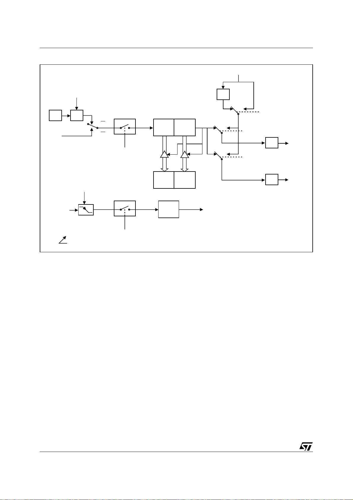
uPSD34xx - STANDARD 8032 TIMER/COUNTERS
Figure 30. Timer 2 in Baud Rate Generator Mode
Timer 1 Overflow
f
OSC
T2 pin
T2X pin
Note: Oscillator frequency is divided by 2,
not 12 like in other timer modes.
÷ 12
C/T2 = 0
C/T2 = 1
Transition
Detector
Note: Availability of additional external interrupt.
Control
TR2
Control
EXEN2
(8 bits)
RCAP2L
TL2
EXF2
TH2
(8 bits)
Reload
RCAP2H
÷ 2
'0'
'1'
'1'
Timer 2 Interrupt
'0'
'0'
'1'
RCLK
TCLK
SMOD
÷ 16
÷ 16
RX CLK
TX CLK
AI09605
82/264

SERIAL UART INTERFACES
uPSD34xx devices provide two standard 8032
UART serial ports.
– The first port, UART0, is connected to pins
RxD0 (P3.0) and TxD0 (P3.1)
– The second port, UART1 is connected to pins
RxD1 (P1.2) and TxD1 (P1.3). UART1 can
optionally be routed to pins P4.2 and P4.3 as
described in Alternate Functions, page 60.
The operation of the two serial ports are the same
and are controlled by two SFRs:
■ SCON0 (Table 47., page 84) for UART0
■ SCON1 (Table 48., page 85) for UART1
Each UART has its own data buffer accessed
through an SFR listed below:
■ SBUF0 for UART0, address 99h
■ SBUF1 for UART1, address D9h
When writing SBU0 or SBUF1, the data automatically loads into the associated UART transmit data
register. When reading this SFR, data comes from
a different physical register, which is the receive
register of the associated UART.
Note: For simplicity in the remaining UART discussions, the suffix “0” or “1” will be dropped when
referring to SFR registers and bits related to
UART0 or UART1, since each UART interface has
identical operation. Example, SBUF0 and SBUF1
will be referred to as just SBUF.
Each UART serial port can be full-duplex, meaning
it can transmit and receive simultaneously. Each
UART is also receive-buffered, meaning it can
commence reception of a second byte before a
previously received byte has been read from the
SBUF Register. However, if the first byte still has
not been read by the time reception of the second
byte is complete, one of the bytes will be lost.
UART Operation Modes
Each UART can operate in one of four modes, one
mode is synchronous, and the others are asynchronous as shown in Table 46.
uPSD34xx - SERIAL UART INTERFACES
Mode 0. Mode 0 provides asynchronous, half-du-
plex operation. Serial data is both transmitted, and
received on the RxD pin. The TxD pin outputs a
shift clock for both transmit and receive directions,
thus the MCU must be the master. Eight bits are
transmitted/received LSB first. The baud rate is
fixed at 1/12 of f
Mode 1. Mode 1 provides standard asynchronous, full-duplex communication using a total of 10
bits per data byte. Data is transmitted through TxD
and received through RxD with: a Start Bit (logic
'0'), eight data bits (LSB first), and a Stop Bit (logic
'1'). Upon receive, the eight data bits go into the
SFR SBUF, and the Stop Bit goes into bit RB8 of
the SFR SCON. The baud rate is variable and derived from overflows of Timer 1 or Timer 2.
Mode 2. Mode 2 provides asynchronous, full-duplex communication using a total of 11 bits per
data byte. Data is transmitted through TxD and received through RxD with: a Start Bit (logic '0');
eight data bits (LSB first); a programmable 9th
data bit; and a Stop Bit (logic '1'). Upon Transmit,
the 9th data bit (from bit TB8 in SCON) can be assigned the value of '0' or '1.' Or, for example, the
Parity Bit (P, in the PSW) could be moved into
TB8. Upon receive, the 9th data bit goes into RB8
in SCON, while the Stop Bit is ignored. The baud
rate is programmable to either 1/32 or 1/64 of
.
f
OSC
Mode 3. Mode 3 is the same as Mode 2 in all respects except the baud rate is variable like it is in
Mode 1.
In all four modes, transmission is initiated by any
instruction that uses SBUF as a destination register. Reception is initiated in Mode 0 by the condition RI = 0 and REN = 1. Reception is initiated in
the other modes by the incoming Start Bit if
REN = 1.
OSC
.
Table 46. UART Operating Modes
Bits of SFR,
Mode Synchronization
0 Synchronous 0 0
1 Asynchronous 0 1 Timer 1 or Timer 2 Overflow 8 1 Start, 1 Stop
2 Asynchronous 1 0
3 Asynchronous 1 1 Timer 1 or Timer 2 Overflow 9 1 Start, 1 Stop
SCON
SM0 SM1
Baud Clock
f
OSC
/32 or f
f
OSC
/12
OSC
/64
Data
Start/Stop Bits See Figure
Bits
8 None
9 1 Start, 1 Stop
Figure
31., page 88
Figure
33., page 90
Figure
35., page 92
Figure
37., page 93
83/264
uPSD34xx - SERIAL UART INTERFACES
Multiprocessor Communications. Modes 2 and
3 have a special provision for multiprocessor communications. In these modes, 9 data bits are received. The 9th one goes into bit RB8, then comes
a stop bit. The port can be programmed such that
when the stop bit is received, the UART interrupt
will be activated only if bit RB8 = 1. This feature is
enabled by setting bit SM2 in SCON. A way to use
this feature in multi-processor systems is as follows: When the master processor wants to transmit a block of data to one of several slaves, it first
sends out an address byte which identifies the target slave. An address byte differs from a data byte
in that the 9th bit is 1 in an address byte and 0 in a
data byte. With SM2 = 1, no slave will be interrupted by a data byte. An address byte, however, will
interrupt all slaves, so that each slave can examine the received byte and see if it is being ad-
dressed. The addressed slave will clear its SM2 bit
and prepare to receive the data bytes that will be
coming. The slaves that were not being addressed
leave their SM2 bits set and go on about their business, ignoring the coming data bytes.
SM2 has no effect in Mode 0, and in Mode 1, SM2
can be used to check the validity of the stop bit. In
a Mode 1 reception, if SM2 = 1, the receive interrupt will not be activated unless a valid stop bit is
received.
Serial Port Control Registers
The SFR SCON0 controls UART0, and SCON1
controls UART1, shown in Table 47 and Table 48.
These registers contain not only the mode selection bits, but also the 9th data bit for transmit and
receive (bits TB8 and RB8), and the UART Interrupt flags, TI and RI.
Table 47. SCON0: Serial Port UART0 Control Register (SFR 98h, reset value 00h)
Bit 7Bit 6Bit 5Bit 4Bit 3Bit 2Bit 1Bit 0
SM0 SM1 SM2 REN TB8 RB8 TI RI
Details
Bit Symbol R/W Definition
7 SM0 R,W Serial Mode Select, See Table 46., page 83. Important, notice bit order
of SM0 and SM1.
6SM1R,W
5SM2R,W
4RENR,W
3TB8R,W
2RB8R,W
1TIR,W
[SM0:SM1] = 00b, Mode 0
[SM0:SM1] = 01b, Mode 1
[SM0:SM1] = 10b, Mode 2
[SM0:SM1] = 11b, Mode 3
Serial Multiprocessor Communication Enable.
Mode 0: SM2 has no effect but should remain 0.
Mode 1: If SM2 = 0 then stop bit ignored. SM2 =1 then RI active if stop
bit = 1.
Mode 2 and 3: Multiprocessor Comm Enable. If SM2=0, 9th bit is
ignored. If SM2=1, RI active when 9th bit = 1.
Receive Enable.
If REN=0, UART reception disabled. If REN=1, reception is enabled
TB8 is assigned to the 9th transmission bit in Mode 2 and 3. Not used in
Mode 0 and 1.
Mode 0: RB8 is not used.
Mode 1: If SM2 = 0, the RB8 is the level of the received stop bit.
Mode 2 and 3: RB8 is the 9th data bit that was received in Mode 2 and
3.
Transmit Interrupt flag.
Causes interrupt at end of 8th bit time when transmitting in Mode 0, or at
beginning of stop bit transmission in other modes. Must clear flag with
firmware.
Receive Interrupt flag.
0RIR,W
84/264
Causes interrupt at end of 8th bit time when receiving in Mode 0, or
halfway through stop bit reception in other modes (see SM2 for
exception). Must clear this flag with firmware.

uPSD34xx - SERIAL UART INTERFACES
Table 48. SCON1: Serial Port UART1 Control Register (SFR D8h, reset value 00h)
Bit 7Bit 6Bit 5Bit 4Bit 3Bit 2Bit 1Bit 0
SM0 SM1 SM2 REN TB8 RB8 TI RI
Details
Bit Symbol R/W Definition
7 SM0 R,W Serial Mode Select, See Table 46., page 83. Important, notice bit order
of SM0 and SM1.
6SM1R,W
5SM2R,W
4RENR,W
3TB8R,W
2RB8R,W
1TIR,W
[SM0:SM1] = 00b, Mode 0
[SM0:SM1] = 01b, Mode 1
[SM0:SM1] = 10b, Mode 2
[SM0:SM1] = 11b, Mode 3
Serial Multiprocessor Communication Enable.
Mode 0: SM2 has no effect but should remain 0.
Mode 1: If SM2 = 0 then stop bit ignored. SM2 =1 then RI active if stop
bit = 1.
Mode 2 and 3: Multiprocessor Comm Enable. If SM2=0, 9th bit is
ignored. If SM2=1, RI active when 9th bit = 1.
Receive Enable.
If REN=0, UART reception disabled. If REN=1, reception is enabled
TB8 is assigned to the 9th transmission bit in Mode 2 and 3. Not used in
Mode 0 and 1.
Mode 0: RB8 is not used.
Mode 1: If SM2 = 0, the RB8 is the level of the received stop bit.
Mode 2 and 3: RB8 is the 9th data bit that was received in Mode 2 and
3.
Transmit Interrupt flag.
Causes interrupt at end of 8th bit time when transmitting in Mode 0, or at
beginning of stop bit transmission in other modes. Must clear flag with
firmware.
Receive Interrupt flag.
0RIR,W
Causes interrupt at end of 8th bit time when receiving in Mode 0, or
halfway through stop bit reception in other modes (see SM2 for
exception). Must clear this flag with firmware.
85/264
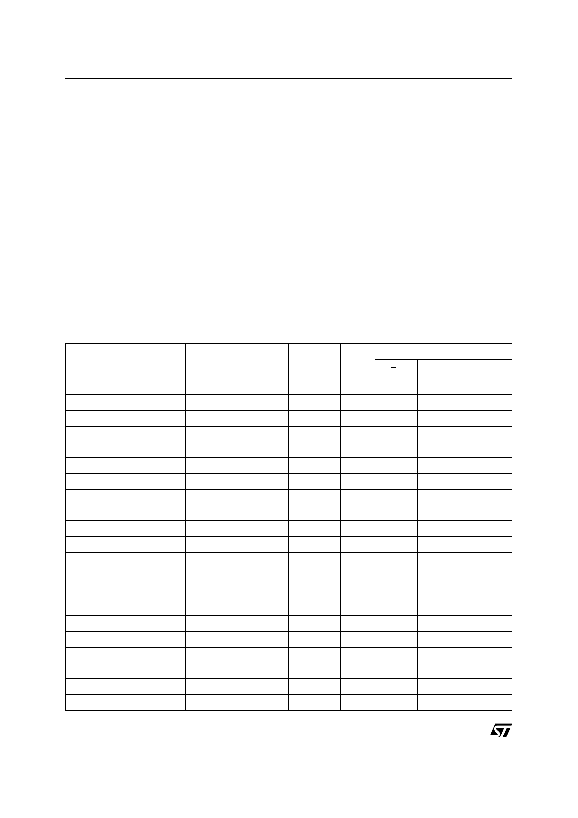
uPSD34xx - SERIAL UART INTERFACES
UART Baud Rates
The baud rate in Mode 0 is fixed:
Mode 0 Baud Rate = f
OSC
/ 12
The baud rate in Mode 2 depends on the value of
the bit SMOD in the SFR named PCON. If SMOD
= 0 (default value), the baud rate is 1/64 the oscillator frequency, f
. If SMOD = 1, the baud rate
OSC
is 1/32 the oscillator frequency.
SMOD
Mode 2 Baud Rate = (2
/ 64) x f
OSC
Baud rates in Modes 1 and 3 are determined by
the Timer 1 or Timer 2 overflow rate.
Using Timer 1 to Generate Baud Rates. When
Timer 1 is used as the baud rate generator (bits
RCLK = 0, TCLK = 0), the baud rates in Modes 1
and 3 are determined by the Timer 1 overflow rate
and the value of SMOD as follows:
Mode 1,3 Baud Rate =
SMOD
(2
/ 32) x (Timer 1 overflow rate)
Table 49. Commonly Used Baud Rates Generated from Timer 1
f
UART Mode
Mode 0 Max 40.0 3.33MHz 3.33MHz 0 X X X X
Mode 2 Max 40.0 1250 k 1250 k 0 1 X X X
Mode 2 Max 40.0 625 k 625 k 0 0 X X X
Modes 1 or 3 40.0 19200 18939 -1.36% 1 0 2 F5
Modes 1 or 3 40.0 9600 9470 -1.36% 1 0 2 EA
Modes 1 or 3 36.0 19200 18570 -2.34% 1 0 2 F6
Modes 1 or 3 33.333 57600 57870 0.47% 1 0 2 FD
Modes 1 or 3 33.333 28800 28934 0.47% 1 0 2 FA
Modes 1 or 3 33.333 19200 19290 0.47% 1 0 2 F7
Modes 1 or 3 33.333 9600 9645 0.47% 1 0 2 EE
Modes 1 or 3 24.0 9600 9615 0.16% 1 0 2 F3
Modes 1 or 3 12.0 4800 4808 0.16% 1 0 2 F3
Modes 1 or 3 11.0592 57600 57600 0 1 0 2 FF
Modes 1 or 3 11.0592 28800 28800 0 1 0 2 FE
Modes 1 or 3 11.0592 19200 19200 0 1 0 2 FD
Modes 1 or 3 11.0592 9600 9600 0 1 0 2 FA
Modes 1 or 3 3.6864 19200 19200 0 1 0 2 FF
Modes 1 or 3 3.6864 9600 9600 0 1 0 2 FE
Modes 1 or 3 1.8432 9600 9600 0 1 0 2 FF
Modes 1 or 3 1.8432 4800 4800 0 1 0 2 FE
OSC
MHz
Desired
Baud Rate
Resultant
Baud Rate
The Timer 1 Interrupt should be disabled in this
application. The Timer itself can be configured for
either “timer” or “counter” operation, and in any of
its 3 running modes. In the most typical applications, it is configured for “timer” operation, in the
Auto-reload Mode (high nibble of the SFR TMOD
= 0010B). In that case the baud rate is given by the
formula:
Mode 1,3 Baud Rate =
SMOD
(2
/ 32) x (f
/ (12 x [256 – (TH1)]))
OSC
Table 49 lists various commonly used baud rates
and how they can be obtained from Timer 1.
Using Timer/Counter 2 to Generate Baud
Rates. See Baud Rate Generator
Mode, page 79.
Timer 1
Timer
Mode in
TMOD
value (hex)
Baud Rate
Deviation
SMOD
bit in
PCON
C/T Bit
in TMOD
TH1
Reload
86/264

More About UART Mode 0
Refer to the block diagram in Figure 31., page 88,
and timing diagram in Figure 32., page 88.
Transmission is initiated by any instruction which
writes to the SFR named SBUF. At the end of a
write operation to SBUF, a 1 is loaded into the 9th
position of the transmit shift register and tells the
TX Control unit to begin a transmission. Transmission begins on the following MCU machine cycle,
when the “SEND” signal is active in Figure 32.
SEND enables the output of the shift register to the
alternate function on the port containing pin RxD,
and also enables the SHIFT CLOCK signal to the
alternate function on the port containing the pin,
TxD. At the end of each SHIFT CLOCK in which
SEND is active, the contents of the transmit shift
register are shifted to the right one position.
As data bits shift out to the right, zeros come in
from the left. When the MSB of the data byte is at
the output position of the shift register, then the '1'
that was initially loaded into the 9th position, is just
to the left of the MSB, and all positions to the left
of that contain zeros. This condition flags the TX
uPSD34xx - SERIAL UART INTERFACES
Control unit to do one last shift, then deactivate
SEND, and then set the interrupt flag TI. Both of
these actions occur at S1P1.
Reception is initiated by the condition REN = 1 and
RI = 0. At the end of the next MCU machine cycle,
the RX Control unit writes the bits 11111110 to the
receive shift register, and in the next clock phase
activates RECEIVE. RECEIVE enables the SHIFT
CLOCK signal to the alternate function on the port
containing the pin, TxD. Each pulse of SHIFT
CLOCK moves the contents of the receive shift
register one position to the left while RECEIVE is
active. The value that comes in from the right is the
value that was sampled at the RxD pin. As data
bits come in from the right, 1s shift out to the left.
When the 0 that was initially loaded into the rightmost position arrives at the left-most position in the
shift register, it flags the RX Control unit to do one
last shift, and then it loads SBUF. After this, RECEIVE is cleared, and the receive interrupt flag RI
is set.
87/264
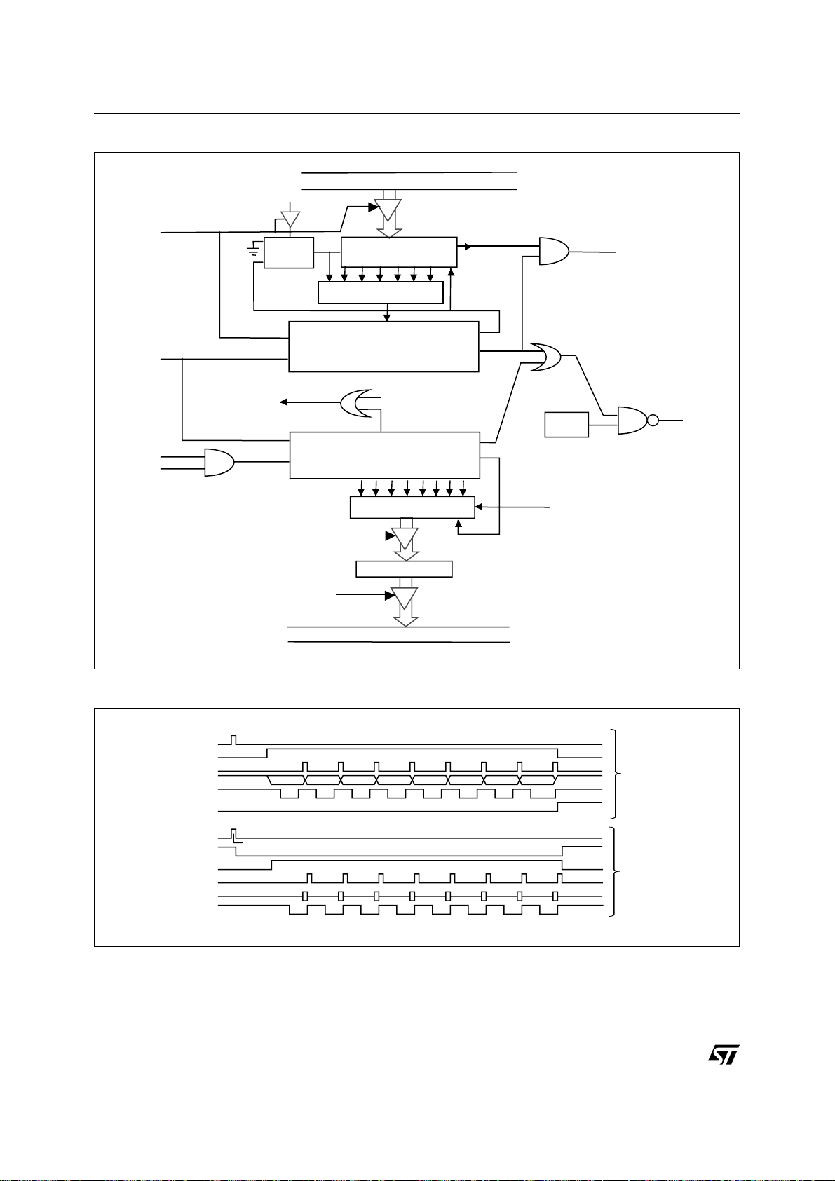
uPSD34xx - SERIAL UART INTERFACES
Figure 31. UART Mode 0, Block Diagram
Internal Bus
Write
to
SBUF
DS
CL
Q
SBUF
Zero Detector
RxD
Pin
Start
f
OSC
/12
REN
R1
Serial
Port
Interrupt
Tx Clock
Rx Clock
Start
Load
SBUF
Read
SBUF
7 6 5 4 3 2 1 0
Figure 32. UART Mode 0, Timing Diagram
Tx Control
T
R
Rx Control
Input Shift Register
SBUF
Internal Bus
Shift
Send
Receive
Shift
Shift
Shift
Clock
RxD
P3.0 Alt
Input
Function
TxD
Pin
AI06824
88/264
Write to SBUF
Send
Shift
RxD (Data Out)
TxD (Shift Clock)
Write to SCON
Receive
Shift
RxD (Data In)
TxD (Shift Clock)
D0 D1 D2 D3 D4 D5 D6 D7
TI
RI
Clear RI
D0 D1 D2 D3 D4 D5 D6 D7
Transmit
Receive
AI06825

More About UART Mode 1
Refer to the block diagram in Figure 33., page 90,
and timing diagram in Figure 34., page 90.
Transmission is initiated by any instruction which
writes to SBUF. At the end of a write operation to
SBUF, a '1' is loaded into the 9th position of the
transmit shift register and flags the TX Control unit
that a transmission is requested. Transmission actually starts at the end of the MCU the machine cycle following the next rollover in the divide-by-16
counter. Thus, the bit times are synchronized to
the divide-by-16 counter, not to the writing of
SBUF. Transmission begins with activation of
SEND which puts the start bit at pin TxD. One bit
time later, DATA is activated, which enables the
output bit of the transmit shift register to pin TxD.
The first shift pulse occurs one bit time after that.
As data bits shift out to the right, zeros are clocked
in from the left. When the MSB of the data byte is
at the output position of the shift register, then the
1 that was initially loaded into the 9th position is
just to the left of the MSB, and all positions to the
left of that contain zeros. This condition flags the
TX Control unit to do one last shift and then deactivates SEND, and sets the interrupt flag, TI. This
occurs at the 10th divide-by-16 rollover after a
write to SBUF.
Reception is initiated by a detected 1-to-0 transition at the pin RxD. For this purpose RxD is sampled at a rate of 16 times whatever baud rate has
been established. When a transition is detected,
the divide-by-16 counter is immediately reset, and
1FFH is written into the input shift register. Resetting the divide-by-16 counter aligns its rollovers
uPSD34xx - SERIAL UART INTERFACES
with the boundaries of the incoming bit times. The
16 states of the counter divide each bit time into
16ths. At the 7th, 8th, and 9th counter states of
each bit time, the bit detector samples the value of
RxD. The value accepted is the value that was
seen in at least 2 of the 3 samples. This is done for
noise rejection. If the value accepted during the
first bit time is not '0,' the receive circuits are reset
and the unit goes back to looking for another '1'-to'0' transition. This is to provide rejection of false
start bits. If the start bit proves valid, it is shifted
into the input shift register, and reception of the reset of the rest of the frame will proceed. As data
bits come in from the right, '1s' shift out to the left.
When the start bit arrives at the left-most position
in the shift register (which in mode 1 is a 9-bit register), it flags the RX Control unit to do one last
shift, load SBUF and RB8, and set the receive interrupt flag RI. The signal to load SBUF and RB8,
and to set RI, will be generated if, and only if, the
following conditions are met at the time the final
shift pulse is generated:
1. RI = 0, and
2. Either SM2 = 0, or the received stop bit = 1.
If either of these two conditions are not met, the re-
ceived frame is irretrievably lost. If both conditions
are met, the stop bit goes into RB8, the 8 data bits
go into SBUF, and RI is activated. At this time,
whether the above conditions are met or not, the
unit goes back to looking for a '1'-to-'0' transition
on pin RxD.
89/264

uPSD34xx - SERIAL UART INTERFACES
Figure 33. UART Mode 1, Block Diagram
SMOD
TCLK
RCLK
Timer1
Overflow
÷2
01
Timer2
Overflow
01
0
1
Write
to
SBUF
RxD
Pin
Sample
1-to-0
Transition
Detector
÷16
Serial
Port
Interrupt
Rx Detector
TB8
DS
CL
Q
Start
Tx Clock
÷16
Rx Clock
Start
Load
SBUF
Read
SBUF
Internal Bus
SBUF
Zero Detector
Tx Control
TI
RI
Rx Control
1FFh
Input Shift Register
SBUF
Shift
Send
Load SBUF
Data
Shift
Shift
TxD
Pin
Figure 34. UART Mode 1, Timing Diagram
Tx Clock
Write to SBUF
Send
Data
90/264
Shift
TxD
Rx Clock
RxD
Bit Detector
Sample Times
Shift
TI
RI
Start Bit
Start Bit
D0 D1 D2 D3 D4 D5 D6 D7
D0 D1 D2 D3 D4 D5 D6 D7
Internal Bus
Stop Bit
Stop Bit
AI06826
Transmit
Receive
AI06843

More About UART Modes 2 and 3
For Mode 2, refer to the block diagram in Figure
35., page 92, and timing diagram in Figure
36., page 92. For Mode 3, refer to the block dia-
gram in Figure 37., page 93, and timing diagram in
Figure 38., page 93.
Keep in mind that the baud rate is programmable
to either 1/32 or 1/64 of f
in Mode 2, but Mode
OSC
3 uses a variable baud rate generated from Timer
1 or Timer 2 rollovers.
The receive portion is exactly the same as in Mode
1. The transmit portion differs from Mode 1 only in
the 9th bit of the transmit shift register.
Transmission is initiated by any instruction which
writes to SBUF. At the end of a write operation to
SBUF, the TB8 Bit is loaded into the 9th position of
the transmit shift register and flags the TX Control
unit that a transmission is requested. Transmission actually starts at the end of the MCU the machine cycle following the next rollover in the divideby-16 counter. Thus, the bit times are synchronized to the divide-by-16 counter, not to the writing
of SBUF. Transmission begins with activation of
SEND which puts the start bit at pin TxD. One bit
time later, DATA is activated, which enables the
output bit of the transmit shift register to pin TxD.
The first shift pulse occurs one bit time after that.
The first shift clocks a '1' (the stop bit) into the 9th
bit position of the shift register. There-after, only
zeros are clocked in. Thus, as data bits shift out to
the right, zeros are clocked in from the left. When
bit TB8 is at the output position of the shift register,
then the stop bit is just to the left of TB8, and all positions to the left of that contain zeros. This condition flags the TX Control unit to do one last shift
and then deactivate SEND, and set the interrupt
uPSD34xx - SERIAL UART INTERFACES
flag, TI. This occurs at the 11th divide-by 16 rollover after writing to SBUF.
Reception is initiated by a detected 1-to-0 transition at pin RxD. For this purpose RxD is sampled
at a rate of 16 times whatever baud rate has been
established. When a transition is detected, the divide-by-16 counter is immediately reset, and 1FFH
is written to the input shift register. At the 7th, 8th,
and 9th counter states of each bit time, the bit detector samples the value of RxD. The value accepted is the value that was seen in at least 2 of
the 3 samples. If the value accepted during the
first bit time is not '0,' the receive circuits are reset
and the unit goes back to looking for another '1'-to'0' transition. If the start bit proves valid, it is shifted
into the input shift register, and reception of the
rest of the frame will proceed. As data bits come in
from the right, '1s' shift out to the left. When the
start bit arrives at the left-most position in the shift
register (which in Modes 2 and 3 is a 9-bit register), it flags the RX Control unit to do one last shift,
load SBUF and RB8, and set the interrupt flag RI.
The signal to load SBUF and RB8, and to set RI,
will be generated if, and only if, the following conditions are met at the time the final shift pulse is
generated:
1. RI = 0, and
2. Either SM2 = 0, or the received 9th data bit = 1.
If either of these conditions is not met, the received
frame is irretrievably lost, and RI is not set. If both
conditions are met, the received 9th data bit goes
into RB8, and the first 8 data bits go into SBUF.
One bit time later, whether the above conditions
were met or not, the unit goes back to looking for
a '1'-to-'0' transition on pin RxD.
91/264

uPSD34xx - SERIAL UART INTERFACES
Figure 35. UART Mode 2, Block Diagram
f
OSC
SMOD
÷2
/32
01
Write
to
SBUF
RxD
Pin
Sample
1-to-0
Transition
Detector
÷16
Serial
Port
Interrupt
Rx Detector
TB8
DS
CL
Q
Start
Tx Clock
÷16
Rx Clock
Start
Load
SBUF
Read
SBUF
Internal Bus
SBUF
Zero Detector
Tx Control
TI
RI
Rx Control
1FFh
Input Shift Register
SBUF
Shift
Send
Load SBUF
Data
Shift
Shift
TxD
Pin
Figure 36. UART Mode 2, Timing Diagram
Tx Clock
Write to SBUF
Send
Data
92/264
Shift
TxD
Stop Bit
Generator
Rx Clock
RxD
Bit Detector
Sample Times
Shift
TI
RI
Start Bit
Start Bit
D0 D1 D2 D3 D4 D5 D6 D7
D0 D1 D2 D3 D4 D5 D6 D7
Internal Bus
TB8
RB8
Stop Bit
Stop Bit
AI06844
Transmit
Receive
AI06845

Figure 37. UART Mode 3, Block Diagram
uPSD34xx - SERIAL UART INTERFACES
SMOD
TCLK
RCLK
Timer1
Overflow
÷2
01
Timer2
Overflow
01
0
1
Write
to
SBUF
RxD
Pin
Sample
1-to-0
Transition
Detector
÷16
Serial
Port
Interrupt
Rx Detector
TB8
DS
CL
Q
Start
Tx Clock
÷16
Rx Clock
Start
Load
SBUF
Read
SBUF
Internal Bus
SBUF
Zero Detector
Tx Control
TI
RI
Rx Control
1FFh
Input Shift Register
SBUF
Shift
Send
Load SBUF
Data
Shift
Shift
TxD
Pin
Figure 38. UART Mode 3, Timing Diagram
Tx Clock
Write to SBUF
Send
Data
Shift
TxD
Stop Bit
Generator
Rx Clock
RxD
Bit Detector
Sample Times
Shift
TI
RI
Start Bit
Start Bit
D0 D1 D2 D3 D4 D5 D6 D7
D0 D1 D2 D3 D4 D5 D6 D7
Internal Bus
TB8
RB8
Stop Bit
Stop Bit
AI06846
Transmit
Receive
AI06847
93/264

uPSD34xx - IrDA INTERFACE
IrDA INTERFACE
uPSD34xx devices provide an internal IrDA interface that will allow the connection of the UART1
serial interface directly to an external infrared
transceiver device. The IrDA interface does this by
automatically shortening the pulses transmitted on
UART1’s TxD1 pin, and stretching the incoming
pulses received on the RxD1 pin. Reference Figures 39 and 40.
When the IrDA interface is enabled, the output signal from UART1’s transmitter logic on pin TxD1 is
Figure 39. IrDA Interface
compliant with the IrDA Physical Layer Link Specification v1.4 (www.irda.org) operating from 1.2k
bps up to 115.2k bps. The pulses received on the
RxD1 pin are stretched by the IrDA interface to be
recognized by UART1’s receiver logic, also adhering to the IrDA specification up to 115.2k bps.
Note: In Figure 40 a logic '0' in the serial data
stream of a UART Frame corresponds to a logic
high pulse in an IR Frame. A logic '1' in a UART
Frame corresponds to no pulse in an IR Frame.
SIRClk
UA RT1
TxD
RxD
uPSD34xx
IrDA
Int er f ac e
Figure 40. Pulse Shaping by the IrDA Interface
UART Frame
Start
Bit
0101 11 100 0
Start
Bit
Data Bits
UART Frame
IR Frame
Data Bits
TxD1-IrDA
Ir DA
Transceiver
Rx D1- IrDA
AI10437
Stop
Bit
Stop
Bit
94/264
0101 11 100 0
IR Frame
Bit Time
Pulse Width = 3/16 Bit Time
AI10438

uPSD34xx - IrDA INTERFACE
The UART1 serial channel can operate in one of
four different modes as shown in Table
46., page 83 in the section, SERIAL UART
INTERFACES, page 83. However, when UART1
is used for IrDA communication, UART1 must operate in Mode 1 only, to be compatible with IrDA
protocol up to 115.2k bps. The IrDA interface will
support baud rates generated from Timer 1 or Timer 2, just like standard UART serial communication, but with one restriction. The transmit baud
rate and receive baud rate must be the same (cannot be different rates as is allowed by standard
UART communications).
The IrDA Interface is disabled after a reset and is
enabled by setting the IRDAEN Bit in the SFR
named IRDACON (Table 50., page 95). When
IrDA is disabled, the UART1's RxD and TxD signals will bypass the internal IrDA logic and instead
they are routed directly to the pins RxD1 and TxD1
respectively. When IrDA is enabled, the IrDA pulse
shaping logic is active and resides between
UART1 and the pins RxD1 and TxD1 as shown in
Figure 39., page 94.
Baud Rate Selection
The IrDA standard only supports 2.4, 9.6, 19.2,
and 115.2kbps. Table Table 52., page 96 informs
the IrDA Interface of the baud rate of UART#2 so
that it can perform pulse modulation properly. It
may not be necessary to implement the BR[3:0]
bits in the IRDACON Register if the IrDA Interface
obtains the proper timing from UART#2.
Table 50. IRDACON Register Bit Definition (SFR CEh, Reset Value 0Fh)
Bit 7 Bit 6 Bit 5 Bit 4 Bit 3 Bit 2 Bit 1 Bit 0
– IRDAEN PULSE CDIV4 CDIV3 CDIV2 CDIV1 CDIV0
Details
Bit Symbol R/W Definition
7 – – Reserved
IrDA Enable
6 IRDAEN RW
5PULSERW
4-0 CDIV[4:0] RW Specify Clock Divider (see Table 53., page 97)
0 = IrDA Interface is disabled
1 = IrDA is enabled, UART1 outputs are disconnected from Port 1 (or
Por t 4)
IrDA Pulse Modulation Select
0 = 1.627µs
1 = 3/16 bit time pulses
Table 51. Baud Rate Selection Register (SFR xxh, reset value xxh)
Bit Symbol R/W Definition
7:4 BR[3:0] R,W Specify Baud Rate (see Table 52)
IrDA Pulse Modulation Select
3:2 PULSE R,W
1:0 IRDAEN R,W
0 = 3/16 bit time pulses (not recommended)
1 = 1.627µs
0 = IrDA Interface is disabled
1 = IrDA is enabled, UART#2 outputs are disconnected from Port 1 (or
Por t 4)
95/264
uPSD34xx - IrDA INTERFACE
Table 52. Baud Rate of UART#2 for IrDA Interface
BR3 BR2 BR1 BR0 Baud Rate (kbps)
0 0 0 0 115.2
000157.5
001038.4
001119.2
010014.4
010112.8
01109.6
01117.2
10004.8
10013.6
10102.4
10111.8
11001.2
96/264
uPSD34xx - IrDA INTERFACE
Pulse Width Selection
The IrDA interface has two ways to modulate the
standard UART1 serial stream:
1. An IrDA data pulse will have a constant pulse
width for any bit time, regardless of the
selected baud rate.
2. An IrDA data pulse will have a pulse width that
is proportional to the the bit time of the
selected baud rate. In this case, an IrDA data
pulse width is 3/16 of its bit time, as shown in
Figure 40., page 94.
The PULSE bit in the SFR named IRDACON determines which method above will be used.
According to the IrDA physical layer specification,
for all baud rates at 115.2k bps and below, the
minimum data pulse width is 1.41µs. For a baud
rate of 115.2k bps, the maximum pulse width
2.23µs. If a constant pulse width is to be used for
all baud rates (PULSE bit = 0), the ideal general
pulse width is 1.63µs, derived from the bit time of
Table 53. Recommended CDIV[4:0] Values to Generate SIRClk (default CDIV[4:0] = 0Fh, 15 decimal)
f
(MHz)
OSC
40.00 16h, 22 decimal 1.82
36.864, or 36.00 14h, 20 decimal 1.84, or 1.80
24.00 0Dh, 13 decimal 1.84
11.059, or 12.00 06h, 6 decimal 1.84, or 2.00
(1)
7.3728
Note: 1. When PULSE bit = 0 (fixed data pulse width), this is minimum recommended f
Value in CDIV[4:0]
04h, 4 decimal 1.84
the fastest baud rate (8.68µs bit time for 115.2k
bps rate), multiplied by the proportion, 3/16.
To produce this fixed data pulse width when the
PULSE bit = 0, a prescaler is needed to generate
an internal reference clock, SIRClk, shown in Fig-
ure 39., page 94. SIRClk is derived by dividing the
oscillator clock frequency, f
using the five bits
OSC,
CDIV[4:0] in the SFR named IRDACON. A divisor
must be chosen to produce a frequency for SIRClk
that lies between 1.34 MHz and 2.13 MHz, but it is
best to choose a divisor value that produces SIRClk frequency as close to 1.83MHz as possible,
because SIRClk at 1.83MHz will produce an fixed
IrDA data pulse width of 1.63µs. Table 53 provides
recommended values for CDIV[4:0] based on several different values of f
OSC
.
For reference, SIRClk of 2.13MHz will generate a
fixed IrDA data pulse width of 1.41µs, and SIRClk
of 1.34MHz will generate a fixed data pulse width
of 2.23µs.
Resulting f
because CDIV[4:0] must be 4 or greater.
OSC
SIRCLK
(MHz)
97/264
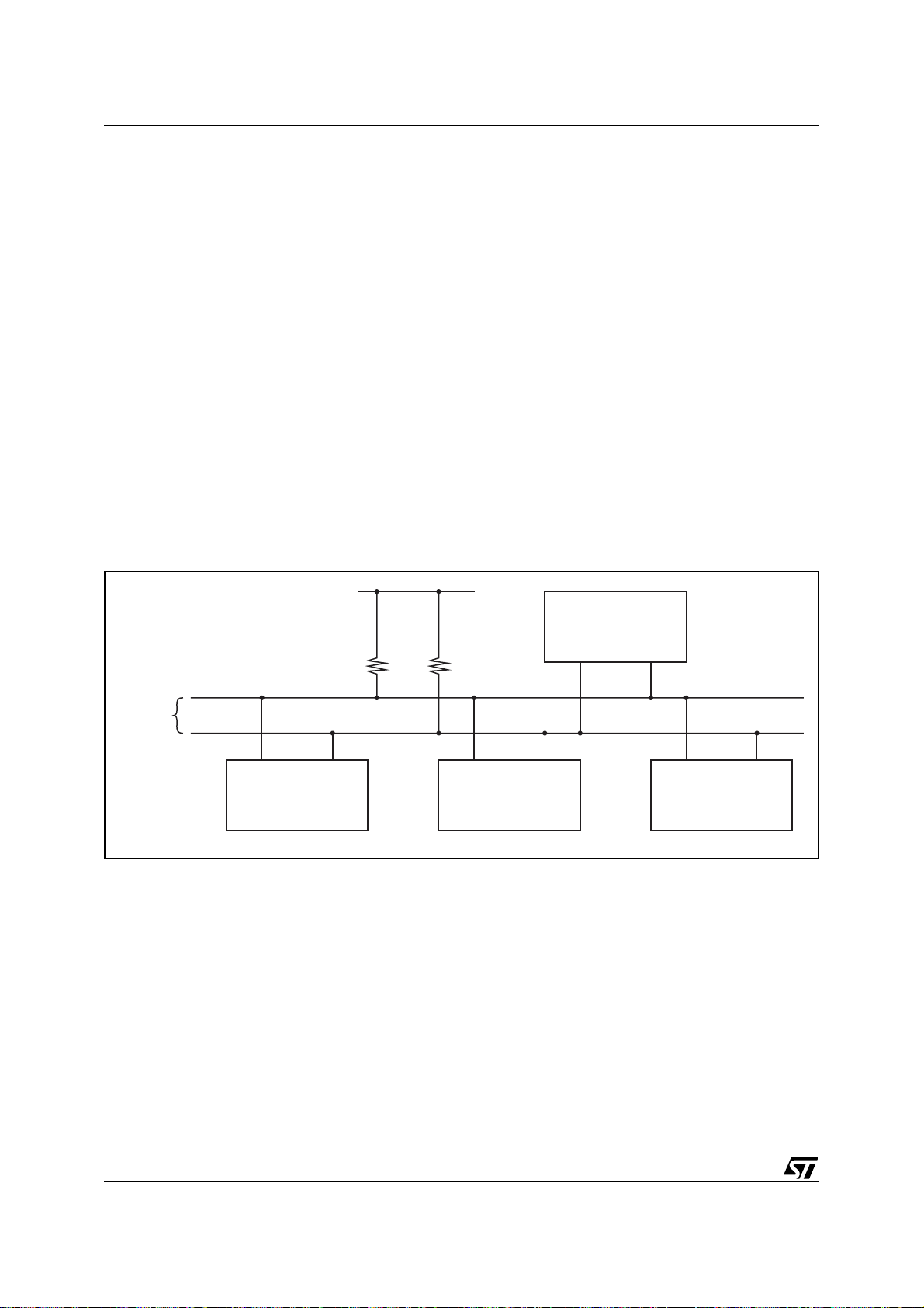
uPSD34xx - I2C INTERFACE
I2C INTERFACE
uPSD34xx devices support one serial I2C interface. This is a two-wire communication channel,
having a bi-directional data signal (SDA, pin P3.6)
and a clock signal (SCL, pin P3.7) based on opendrain line drivers, requiring external pull-up resistors, R
Figure 41).
2
I
Byte-wide data is transferred, MSB first, between
a Master device and a Slave device on two wires.
More than one bus Master is allowed, but only one
Master may control the bus at any given time. Data
is not lost when another Master requests the use
of a busy bus because I
tection and arbitration. The bus Master initiates all
data movement and generates the clock that permits the transfer. Once a transfer is initiated by the
Master, any device addressed is considered a
Slave. Automatic clock synchronization allows I
devices with different bit rates to communicate on
the same physical bus. A single device can play
Figure 41. Typical I
, each with a typical value of 4.7kΩ (see
P
C Interface Main Features
2
C supports collision de-
2
C Bus Configuration
VCC or V
DD
2
(1)
the role of Master or Slave, or a single device can
be a Slave only. Each Slave device on the bus has
a unique address, and a general broadcast address is also available. A Master or Slave device
has the ability to suspend data transfers if the device needs more time to transmit or receive data.
2
C interface has the following features:
This I
– Serial I/O Engine (SIOE): serial/parallel
conversion; bus arbitration; clock generation
and synchronization; and handshaking are all
performed in hardware
– Interrupt or Polled operation
– Multi-master capability
– 7-bit Addressing
2
– Supports standard speed I
100kHz), fast mode I
and high-speed mode I
C
833kHz)
2
C (SCL up to
C (101KHz to 400kHz),
2
C (401KHz to
Device with I2C
R
P
SDA
I2C BUS
Note: 1. For 3.3V system, connect RP to 3.3V VCC. For 5.0V system, connect RP to 5.0V VDD.
SCL
SDA/P3.6 SCL/P3.7
uPSD33XX(V)
R
P
Device with I2C
Interface
Interface
Device with I2C
Interface
AI09623
98/264

Communication Flow
2
I
C data flow control is based on the fact that all
2
C compatible devices will drive the bus lines with
I
open-drain (or open-collector) line drivers pulled
up with external resistors, creating a wired-AND
situation. This means that either bus line (SDA or
SCL) will be at a logic '1' level only when no I
2
C device is actively driving the line to logic '0.' The logic
for handshaking, arbitration, synchronization, and
collision detection is implemented by each I
2
C device having:
1. The ability to hold a line low against the will of
the other devices who are trying to assert the
line high.
2. The ability of a device to detect that another
device is driving the line low against its will.
Assert high means the driver releases the line and
external pull-ups passively raise the signal to logic
'1.' Holding low means the open-drain driver is
actively pulling the signal to ground for a logic '0.'
For example, if a Slave device cannot transmit or
receive a byte because it is distracted by and interrupt or it has to wait for some process to complete,
it can hold the SCL clock line low. Even though the
Master device is generating the SCL clock, the
Master will sense that the Slave is holding the SCL
line low against the will of the Master, indicating
that the Master must wait until the Slave releases
SCL before proceeding with the transfer.
Another example is when two Master devices try
to put information on the bus simultaneously, the
first one to release the SDA data line looses arbitration while the winner continues to hold SDA low.
Two types of data transfers are possible with I
depending on the R/W
bit, see Figure
2
42., page 100.
1. Data transfer from Master Transmitter to
Slave Receiver (R/W
= 0). In this case, the
Master generates a START condition on the
bus and it generates a clock signal on the SCL
line. Then the Master transmits the first byte
on the SDA line containing the 7-bit Slave
address plus the R/W
bit. The Slave who owns
that address will respond with an acknowledge
bit on SDA, and all other Slave devices will not
respond. Next, the Master will transmit a data
byte (or bytes) that the addressed Slave must
receive. The Slave will return an acknowledge
bit after each data byte it successfully
receives. After the final byte is transmitted by
the Master, the Master will generate a STOP
condition on the bus, or it will generate a RE-
uPSD34xx - I2C INTERFACE
START conditon and begin the next transfer.
There is no limit to the number of bytes that
can be transmitted during a transfer session.
2. Data transfer from Slave Transmitter to
Master Receiver (R/W
Master generates a START condition on the
bus and it generates a clock signal on the SCL
line. Then the Master transmits the first byte
on the SDA line containing the 7-bit Slave
address plus the R/W
that address will respond with an acknowledge
bit on SDA, and all other Slave devices will not
respond. Next, the addressed Slave will
transmit a data byte (or bytes) to the Master.
The Master will return an acknowledge bit
after each data byte it successfully receives,
unless it is the last byte the Master desires. If
so, the Master will not acknowledge the last
byte and from this, the Slave knows to stop
transmitting data bytes to the Master. The
Master will then generate a STOP condition on
the bus, or it will generate a RE-START
conditon and begin the next transfer. There is
no limit to the number of bytes that can be
transmitted during a transfer session.
A few things to know related to these transfers:
– Either the Master or Slave device can hold the
SCL clock line low to indicate it needs more
time to handle a byte transfer. An indefinite
holding period is possible.
– A START condition is generated by a Master
and recognized by a Slave when SDA has a 1-
C
to-0 transition while SCL is high (Figure
42., page 100).
– A STOP condition is generated by a Master
and recognized by a Slave when SDA has a 0-
to1 transition while SCL is high (Figure
42., page 100).
– A RE-START (repeated START) condition
generated by a Master can have the same
function as a STOP condition when starting
another data transfer immediately following
the previous data transfer (Figure
42., page 100).
– When transferring data, the logic level on the
SDA line must remain stable while SCL is
high, and SDA can change only while SCL is
low. However, when not transferring data,
SDA may change state while SCL is high,
which creates the START and STOP bus
conditions.
= 1). In this case, the
bit. The Slave who owns
99/264
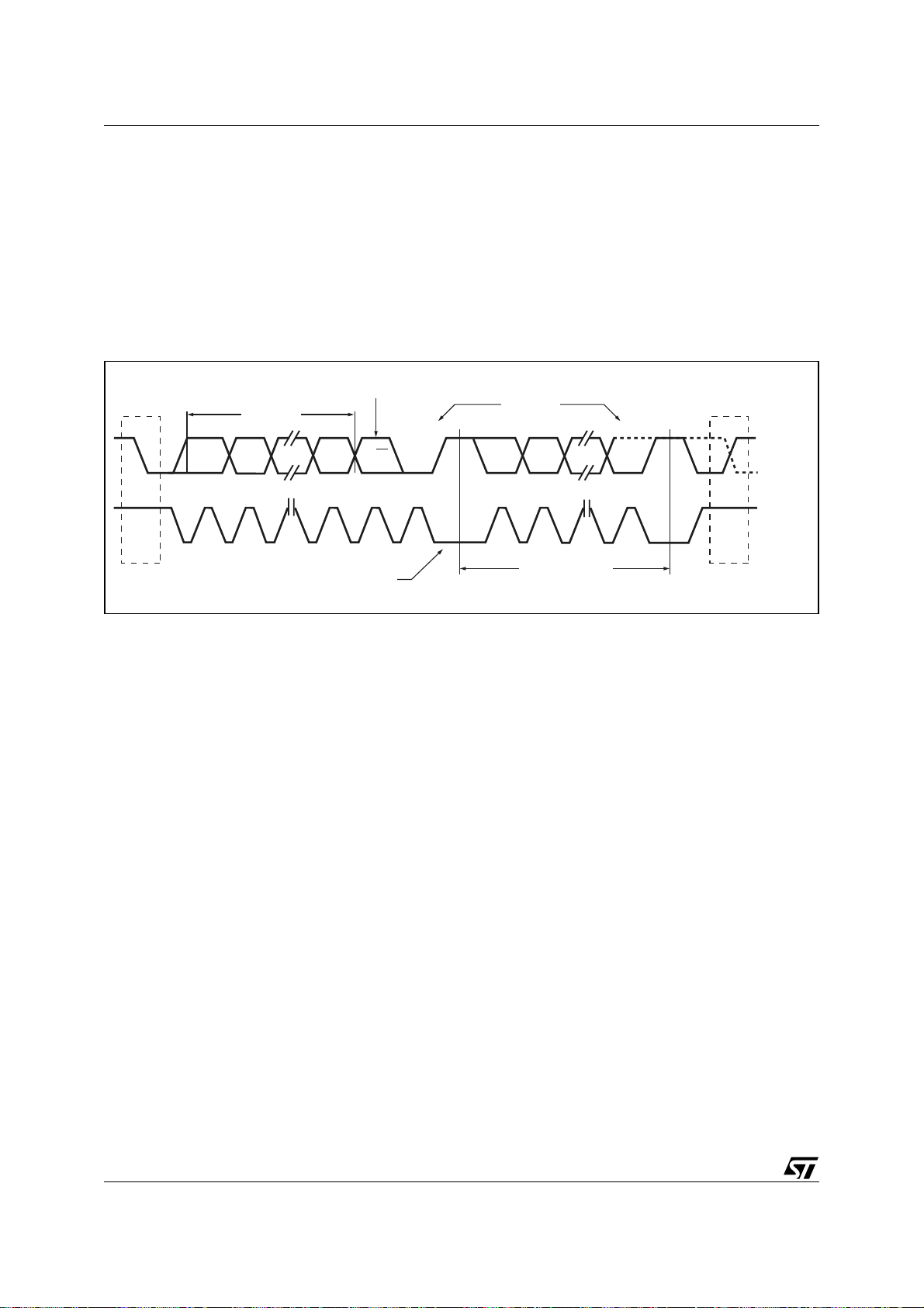
uPSD34xx - I2C INTERFACE
– An Acknowlegde bit is generated from a
Master or a Slave by driving SDA low during
the “ninth” bit time, just following each 8-bit
byte that is transfered on the bus (Figure
42., page 100). A Non-Acknowledge occurs
when SDA is asserted high during the ninth bit
time. All byte transfers on the I
2
C bus include
a 9th bit time reserved for an Acknowlege
(ACK) or Non-Acknowledge (NACK).
2
Figure 42. Data Transfer on an I
7-bit Slave
Address
MSB
12 78 93-6 1 2 93-8
Start
Condition
Clock can be held low
C Bus
READ/WRITE
Indicator
R/W
to stall transfer.
ACK
– An additional Master device that desires to
control the bus should wait until the bus is not
busy before generating a START condition so
that a possible Slave operation is not
interrupted.
– If two Master devices both try to generate a
START condition simultaneously, the Master
who looses arbitration will switch immediately
to Slave mode so it can recoginize its own
Slave address should it appear on the bus.
Acknowledge
bits from
receiver
NACK
MSB
ACK
Repeated if more
data bytes are
transferred.
Stop
Condition
Repeated
Start
Condition
AI09625
100/264
 Loading...