

ST uPSD3312D-40T6, uPSD3312DV-40T6, uPSD3333D-40T6, uPSD3333DV-40T6, uPSD3333D-40U6 User Manual
...
查询UPSD3312D-40T6T供应商
Fast 8032 MCU with Programmable Logic
FEAT URES SUM MARY
■ FAST 8-BIT TURBO 8032 MCU, 40MHz
– Advanced core, 4-clocks per instruction
– 10 MIPs peak performance at 40MHz (5V)
– JTAG Debug and In-System
Programming
– Branch Cache & 6 instruction Prefetch
Queue
– Dual XDATA pointers with auto incr & decr
– Compatible with 3rd party 8051 tools
■ DUAL FLASH MEMORIES WITH MEMORY
MANAGEMENT
– Place either memory into 8032 program
address space or data address space
– READ-while-WRITE operation for In-
Application Programming and EEPR OM
emulation
– Single voltage program and erase
– 100K guarante ed eras e cycle s, 15-year
retention
■ CLOCK, RESET, AND SUPPLY
MANAGEMENT
– SRAM is Battery Backup capable
– Flexible 8-level CPU clock divider register
– Normal, Idle, and Power Down Modes
– Power-on and Low Voltage reset
supervisor
– Programmable Watchdog Timer
■ PROGRAMMABLE LOGIC, GENERAL
PURPOSE
– 16 macrocells
– Create shifters, sta te machines, chip-
selects, glue-logic to keypads, panels,
LCDs, others
■ COMMUNICATION INTERFACES
2
C Master/Slave controller, 833KHz
–I
– SPI Master controller, 10MHz
– Two UARTs with independent baud rate
– IrDA protocol support up to 115K baud
– Up to 46 I/O, 5V tolerant on 3.3V
uPSD33xxV
uPSD33xx
Turbo Series
PRELIMINARY DATA
Figure 1. Packages
TQFP52 (T)
52-lead, Thin,
Quad, Flat
TQFP80 (U)
80-lead, Thin,
Quad, Flat
■ A/D CONVERTER
– Eight Channels, 10-bit resolution, 6µs
■ TIMERS AND INTERRUPTS
– Three 8032 standard 16-bit timers
– Programmable Counter Array (PCA), six
16-bit modules for PWM, CAPCOM, and
timers
– 8/10/16-bit PWM operation
– 11 Interrupt sources with two external
interrupt pins
■ OPERATING VOLTAGE SOURCE (±10%)
– 5V devices use both 5.0V and 3.3V
sources
– 3.3V devices use only 3.3V source
January 2005
This is preliminary information on a new product now in development or undergoing evaluation. Details are subject to change without notice.
1/231
uPSD33xx
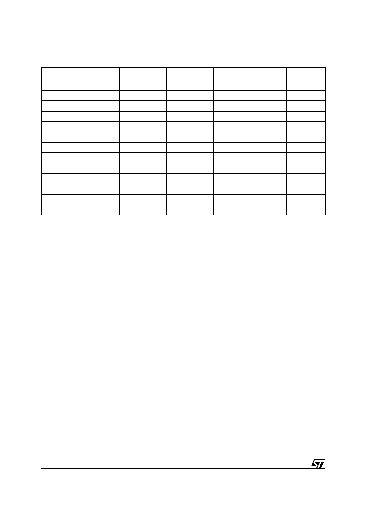
Table 1. Device Summary
1st
Part Number
uPSD3312D-40T6 64K 16K 2K 37 No 3.3V 5.0V TQFP52 –40°C to 85°C
uPSD3312DV-40T6 64K 16K 2K 37 No 3.3V 3.3V TQFP52 –40°C to 85°C
uPSD3333D-40T6 128K 32K 8K 37 No 3.3V 5.0V TQFP52 –40°C to 85°C
uPSD3333DV-40T6 128K 32K 8K 37 No 3.3V 3.3V TQFP52 –40°C to 85°C
uPSD3333D-40U6 128K 32K 8K 46 Yes 3.3V 5.0V TQFP80 –40°C to 85°C
uPSD3333DV-40U6 128K 32K 8K 46 Yes 3.3V 3.3V TQFP80 –40°C to 85°C
uPSD3334D-40U6 256K 32K 8K 46 Yes 3.3V 5.0V TQFP80 –40°C to 85°C
uPSD3334DV-40U6 256K 32K 8K 46 Yes 3.3V 3.3V TQFP80 –40°C to 85°C
uPSD3354D-40T6 256K 32K 32K 37 No 3.3V 5.0V TQFP52 –40°C to 85°C
uPSD3354DV-40T6 256K 32K 32K 37 No 3.3V 3.3V TQFP52 –40°C to 85°C
uPSD3354D-40U6 256K 32K 32K 46 Yes 3.3V 5.0V TQFP80 –40°C to 85°C
uPSD3354DV-40U6 256K 32K 32K 46 Yes 3.3V 3.3V TQFP80 –40°C to 85°C
Flash
(bytes)
2nd
Flash
(bytes)
SRAM
(bytes)
GPIO
8032
Bus
V
CC
V
DD
Pkg. Temp.
2/231

uPSD33xx
TABLE OF CONTENTS
FEATURES SUMMARY . . . . . . . . . . . . . . . . . . . . . . . . . . . . . . . . . . . . . . . . . . . . . . . . . . . . . . . . . . . . . 1
SUMMARY DESCRIPTION. . . . . . . . . . . . . . . . . . . . . . . . . . . . . . . . . . . . . . . . . . . . . . . . . . . . . . . . . . . 7
PIN DESCRIPTIONS. . . . . . . . . . . . . . . . . . . . . . . . . . . . . . . . . . . . . . . . . . . . . . . . . . . . . . . . . . . . . . . . 8
uPSD33xx HARDWARE DESCRIPTION . . . . . . . . . . . . . . . . . . . . . . . . . . . . . . . . . . . . . . . . . . . . . . . 13
MEMORY ORGANIZATION . . . . . . . . . . . . . . . . . . . . . . . . . . . . . . . . . . . . . . . . . . . . . . . . . . . . . . . . . 15
Internal Memory (MCU Module, Standard 8032 Memory: DATA, IDATA, SFR) . . . . . . . . . . . . 16
External Memory (PSD Module: Program memory, Data memory). . . . . . . . . . . . . . . . . . . . . . 16
8032 MCU CORE PERFORMANCE ENHANCEMENTS . . . . . . . . . . . . . . . . . . . . . . . . . . . . . . . . . . . 17
Pre-Fetch Queue (PFQ) and Branch Cache (BC) . . . . . . . . . . . . . . . . . . . . . . . . . . . . . . . . . . . . 19
PFQ Example, Multi-cycle Instructions. . . . . . . . . . . . . . . . . . . . . . . . . . . . . . . . . . . . . . . . . . . . 19
Aggregate Performance . . . . . . . . . . . . . . . . . . . . . . . . . . . . . . . . . . . . . . . . . . . . . . . . . . . . . . . . 19
MCU MODULE DISCRIPTION . . . . . . . . . . . . . . . . . . . . . . . . . . . . . . . . . . . . . . . . . . . . . . . . . . . . . . . 21
8032 MCU REGISTERS . . . . . . . . . . . . . . . . . . . . . . . . . . . . . . . . . . . . . . . . . . . . . . . . . . . . . . . . . . . . 21
Stack Pointer (SP) . . . . . . . . . . . . . . . . . . . . . . . . . . . . . . . . . . . . . . . . . . . . . . . . . . . . . . . . . . . . . 21
Data Pointer (DPTR) . . . . . . . . . . . . . . . . . . . . . . . . . . . . . . . . . . . . . . . . . . . . . . . . . . . . . . . . . . . 21
Program Counter (PC). . . . . . . . . . . . . . . . . . . . . . . . . . . . . . . . . . . . . . . . . . . . . . . . . . . . . . . . . . 21
Accumulator (ACC) . . . . . . . . . . . . . . . . . . . . . . . . . . . . . . . . . . . . . . . . . . . . . . . . . . . . . . . . . . . . 21
B Register (B). . . . . . . . . . . . . . . . . . . . . . . . . . . . . . . . . . . . . . . . . . . . . . . . . . . . . . . . . . . . . . . . . 21
General Purpose Registers (R0 - R7). . . . . . . . . . . . . . . . . . . . . . . . . . . . . . . . . . . . . . . . . . . . . . 22
Program Status Word (PSW) . . . . . . . . . . . . . . . . . . . . . . . . . . . . . . . . . . . . . . . . . . . . . . . . . . . .22
SPECIAL FUNCTION REGISTERS (SFR) . . . . . . . . . . . . . . . . . . . . . . . . . . . . . . . . . . . . . . . . . . . . . . 23
8032 ADDRESSING MODES . . . . . . . . . . . . . . . . . . . . . . . . . . . . . . . . . . . . . . . . . . . . . . . . . . . . . . . . 30
Register Addressing . . . . . . . . . . . . . . . . . . . . . . . . . . . . . . . . . . . . . . . . . . . . . . . . . . . . . . . . . . . 30
Direct Addressing . . . . . . . . . . . . . . . . . . . . . . . . . . . . . . . . . . . . . . . . . . . . . . . . . . . . . . . . . . . . . 30
Register Indirect Addressing . . . . . . . . . . . . . . . . . . . . . . . . . . . . . . . . . . . . . . . . . . . . . . . . . . . . 30
Immediate Addressing . . . . . . . . . . . . . . . . . . . . . . . . . . . . . . . . . . . . . . . . . . . . . . . . . . . . . . . . . 3 0
External Direct Addressing . . . . . . . . . . . . . . . . . . . . . . . . . . . . . . . . . . . . . . . . . . . . . . . . . . . . . 30
External Indirect Addressing . . . . . . . . . . . . . . . . . . . . . . . . . . . . . . . . . . . . . . . . . . . . . . . . . . . . 30
Indexed Addressing . . . . . . . . . . . . . . . . . . . . . . . . . . . . . . . . . . . . . . . . . . . . . . . . . . . . . . . . . . . 31
Relative Addressing . . . . . . . . . . . . . . . . . . . . . . . . . . . . . . . . . . . . . . . . . . . . . . . . . . . . . . . . . . . 31
Absolute Addressing . . . . . . . . . . . . . . . . . . . . . . . . . . . . . . . . . . . . . . . . . . . . . . . . . . . . . . . . . . 31
Long Addressing. . . . . . . . . . . . . . . . . . . . . . . . . . . . . . . . . . . . . . . . . . . . . . . . . . . . . . . . . . . . . . 31
Bit Addressing. . . . . . . . . . . . . . . . . . . . . . . . . . . . . . . . . . . . . . . . . . . . . . . . . . . . . . . . . . . . . . . . 31
uPSD33xx INSTRUCTION SET SUMMARY . . . . . . . . . . . . . . . . . . . . . . . . . . . . . . . . . . . . . . . . . . . . 32
3/231

uPSD33xx
DUAL DATA POINTERS. . . . . . . . . . . . . . . . . . . . . . . . . . . . . . . . . . . . . . . . . . . . . . . . . . . . . . . . . . . . 37
Data Pointer Control Register, DPTC (85h). . . . . . . . . . . . . . . . . . . . . . . . . . . . . . . . . . . . . . . . . 37
Data Pointer Mode Register, DPTM (86h) . . . . . . . . . . . . . . . . . . . . . . . . . . . . . . . . . . . . . . . . . . 38
DEBUG UNIT. . . . . . . . . . . . . . . . . . . . . . . . . . . . . . . . . . . . . . . . . . . . . . . . . . . . . . . . . . . . . . . . . . . . . 39
INTERRUPT SYSTEM . . . . . . . . . . . . . . . . . . . . . . . . . . . . . . . . . . . . . . . . . . . . . . . . . . . . . . . . . . . . . . 40
Individual Interrupt Sources . . . . . . . . . . . . . . . . . . . . . . . . . . . . . . . . . . . . . . . . . . . . . . . . . . . . . 43
MCU CLOCK GENERATION . . . . . . . . . . . . . . . . . . . . . . . . . . . . . . . . . . . . . . . . . . . . . . . . . . . . . . . . 46
MCU_CLK. . . . . . . . . . . . . . . . . . . . . . . . . . . . . . . . . . . . . . . . . . . . . . . . . . . . . . . . . . . . . . . . . . . . 46
PERIPH_CLK . . . . . . . . . . . . . . . . . . . . . . . . . . . . . . . . . . . . . . . . . . . . . . . . . . . . . . . . . . . . . . . . . 46
POWER SAVING MODES . . . . . . . . . . . . . . . . . . . . . . . . . . . . . . . . . . . . . . . . . . . . . . . . . . . . . . . . . . 48
Idle Mode . . . . . . . . . . . . . . . . . . . . . . . . . . . . . . . . . . . . . . . . . . . . . . . . . . . . . . . . . . . . . . . . . . . . 48
Power-down Mode. . . . . . . . . . . . . . . . . . . . . . . . . . . . . . . . . . . . . . . . . . . . . . . . . . . . . . . . . . . . . 4 8
Reduced Frequency Mode . . . . . . . . . . . . . . . . . . . . . . . . . . . . . . . . . . . . . . . . . . . . . . . . . . . . . . 48
OSCILLATOR AND EXTERNAL COMPONENTS . . . . . . . . . . . . . . . . . . . . . . . . . . . . . . . . . . . . . . . . 51
I/O PORTS of MCU MODULE. . . . . . . . . . . . . . . . . . . . . . . . . . . . . . . . . . . . . . . . . . . . . . . . . . . . . . . . 5 3
MCU Port Operating Modes . . . . . . . . . . . . . . . . . . . . . . . . . . . . . . . . . . . . . . . . . . . . . . . . . . . . . 53
MCU BUS INTERFACE. . . . . . . . . . . . . . . . . . . . . . . . . . . . . . . . . . . . . . . . . . . . . . . . . . . . . . . . . . . . . 6 2
Bus Read Cycles (PSEN or RD) . . . . . . . . . . . . . . . . . . . . . . . . . . . . . . . . . . . . . . . . . . . . . . . . . .62
Bus Write Cycles (WR) . . . . . . . . . . . . . . . . . . . . . . . . . . . . . . . . . . . . . . . . . . . . . . . . . . . . . . . . . 6 2
Controlling the PFQ and BC . . . . . . . . . . . . . . . . . . . . . . . . . . . . . . . . . . . . . . . . . . . . . . . . . . . . . 62
SUPERVISORY FUNCTIONS. . . . . . . . . . . . . . . . . . . . . . . . . . . . . . . . . . . . . . . . . . . . . . . . . . . . . . . . 65
External Reset Input Pin, RESET_IN . . . . . . . . . . . . . . . . . . . . . . . . . . . . . . . . . . . . . . . . . . . . . . 65
Low V
Voltage Detect, LVD. . . . . . . . . . . . . . . . . . . . . . . . . . . . . . . . . . . . . . . . . . . . . . . . . . . . 66
CC
Power-up Reset . . . . . . . . . . . . . . . . . . . . . . . . . . . . . . . . . . . . . . . . . . . . . . . . . . . . . . . . . . . . . . . 66
JTAG Debug Reset . . . . . . . . . . . . . . . . . . . . . . . . . . . . . . . . . . . . . . . . . . . . . . . . . . . . . . . . . . . . 66
Watchdog Timer, WDT . . . . . . . . . . . . . . . . . . . . . . . . . . . . . . . . . . . . . . . . . . . . . . . . . . . . . . . . . 66
STANDARD 8032 TIMER/COUNTERS . . . . . . . . . . . . . . . . . . . . . . . . . . . . . . . . . . . . . . . . . . . . . . . . 69
Standard Timer SFRs . . . . . . . . . . . . . . . . . . . . . . . . . . . . . . . . . . . . . . . . . . . . . . . . . . . . . . . . . . 69
Clock Sources . . . . . . . . . . . . . . . . . . . . . . . . . . . . . . . . . . . . . . . . . . . . . . . . . . . . . . . . . . . . . . . . 69
SFR, TCON. . . . . . . . . . . . . . . . . . . . . . . . . . . . . . . . . . . . . . . . . . . . . . . . . . . . . . . . . . . . . . . . . . . 7 1
SFR, TMOD. . . . . . . . . . . . . . . . . . . . . . . . . . . . . . . . . . . . . . . . . . . . . . . . . . . . . . . . . . . . . . . . . . . 71
Timer 0 and Timer 1 Operating Modes . . . . . . . . . . . . . . . . . . . . . . . . . . . . . . . . . . . . . . . . . . . . 71
Timer 2 . . . . . . . . . . . . . . . . . . . . . . . . . . . . . . . . . . . . . . . . . . . . . . . . . . . . . . . . . . . . . . . . . . . . . . 74
SERIAL UART INTERFACES. . . . . . . . . . . . . . . . . . . . . . . . . . . . . . . . . . . . . . . . . . . . . . . . . . . . . . . . 81
UART Operation Modes . . . . . . . . . . . . . . . . . . . . . . . . . . . . . . . . . . . . . . . . . . . . . . . . . . . . . . . . 81
4/231

uPSD33xx
Serial Port Control Registers . . . . . . . . . . . . . . . . . . . . . . . . . . . . . . . . . . . . . . . . . . . . . . . . . . . . 82
UART Baud Rates . . . . . . . . . . . . . . . . . . . . . . . . . . . . . . . . . . . . . . . . . . . . . . . . . . . . . . . . . . . . . 8 4
More About UART Mode 0 . . . . . . . . . . . . . . . . . . . . . . . . . . . . . . . . . . . . . . . . . . . . . . . . . . . . . . 85
More About UART Mode 1 . . . . . . . . . . . . . . . . . . . . . . . . . . . . . . . . . . . . . . . . . . . . . . . . . . . . . . 87
More About UART Modes 2 and 3 . . . . . . . . . . . . . . . . . . . . . . . . . . . . . . . . . . . . . . . . . . . . . . . . 89
IrDA INTERFACE . . . . . . . . . . . . . . . . . . . . . . . . . . . . . . . . . . . . . . . . . . . . . . . . . . . . . . . . . . . . . . . . . 92
Pulse Width Selection. . . . . . . . . . . . . . . . . . . . . . . . . . . . . . . . . . . . . . . . . . . . . . . . . . . . . . . . . . 94
2
I
C INTERFACE . . . . . . . . . . . . . . . . . . . . . . . . . . . . . . . . . . . . . . . . . . . . . . . . . . . . . . . . . . . . . . . . . . 95
I2C Interface Main Features . . . . . . . . . . . . . . . . . . . . . . . . . . . . . . . . . . . . . . . . . . . . . . . . . . . . . 95
Communication Flow . . . . . . . . . . . . . . . . . . . . . . . . . . . . . . . . . . . . . . . . . . . . . . . . . . . . . . . . . . 96
Operating Modes . . . . . . . . . . . . . . . . . . . . . . . . . . . . . . . . . . . . . . . . . . . . . . . . . . . . . . . . . . . . . . 98
Bus Arbitration . . . . . . . . . . . . . . . . . . . . . . . . . . . . . . . . . . . . . . . . . . . . . . . . . . . . . . . . . . . . . . . 98
Clock Synchronization . . . . . . . . . . . . . . . . . . . . . . . . . . . . . . . . . . . . . . . . . . . . . . . . . . . . . . . . . 98
General Call Address . . . . . . . . . . . . . . . . . . . . . . . . . . . . . . . . . . . . . . . . . . . . . . . . . . . . . . . . . . 98
Serial I/O Engine (SIOE) . . . . . . . . . . . . . . . . . . . . . . . . . . . . . . . . . . . . . . . . . . . . . . . . . . . . . . . . 99
2
I
C Interface Control Register (S1CON) . . . . . . . . . . . . . . . . . . . . . . . . . . . . . . . . . . . . . . . . . . 100
2
I
C Interface Status Register (S1STA). . . . . . . . . . . . . . . . . . . . . . . . . . . . . . . . . . . . . . . . . . . . 102
I2C Data Shift Register (S1DAT). . . . . . . . . . . . . . . . . . . . . . . . . . . . . . . . . . . . . . . . . . . . . . . . . 104
2
I
C Address Register (S1ADR). . . . . . . . . . . . . . . . . . . . . . . . . . . . . . . . . . . . . . . . . . . . . . . . . . 104
2
I
C START Sample Setting (S1SETUP) . . . . . . . . . . . . . . . . . . . . . . . . . . . . . . . . . . . . . . . . . . . 105
2
I
C Operating Sequences . . . . . . . . . . . . . . . . . . . . . . . . . . . . . . . . . . . . . . . . . . . . . . . . . . . . . . 108
SPI (SYNCHRONOUS PERIPHERAL INTERFACE) . . . . . . . . . . . . . . . . . . . . . . . . . . . . . . . . . . . . . 112
SPI Bus Features and Communication Flow . . . . . . . . . . . . . . . . . . . . . . . . . . . . . . . . . . . . . . 113
Full-Duplex Operation. . . . . . . . . . . . . . . . . . . . . . . . . . . . . . . . . . . . . . . . . . . . . . . . . . . . . . . . . 113
Bus-Level Activity . . . . . . . . . . . . . . . . . . . . . . . . . . . . . . . . . . . . . . . . . . . . . . . . . . . . . . . . . . . . 113
SPI SFR Registers. . . . . . . . . . . . . . . . . . . . . . . . . . . . . . . . . . . . . . . . . . . . . . . . . . . . . . . . . . . . 115
SPI Configuration . . . . . . . . . . . . . . . . . . . . . . . . . . . . . . . . . . . . . . . . . . . . . . . . . . . . . . . . . . . . 1 1 6
Dynamic Control . . . . . . . . . . . . . . . . . . . . . . . . . . . . . . . . . . . . . . . . . . . . . . . . . . . . . . . . . . . . . 116
ANALOG-TO-DIGITAL CONVERTOR (ADC) . . . . . . . . . . . . . . . . . . . . . . . . . . . . . . . . . . . . . . . . . . 120
Port 1 ADC Channel Selects. . . . . . . . . . . . . . . . . . . . . . . . . . . . . . . . . . . . . . . . . . . . . . . . . . . . 120
PROGRAMMABLE COUNTER ARRAY (PCA) WITH PWM . . . . . . . . . . . . . . . . . . . . . . . . . . . . . . . 123
PCA Block . . . . . . . . . . . . . . . . . . . . . . . . . . . . . . . . . . . . . . . . . . . . . . . . . . . . . . . . . . . . . . . . . . 123
PCA Clock Selection. . . . . . . . . . . . . . . . . . . . . . . . . . . . . . . . . . . . . . . . . . . . . . . . . . . . . . . . . . 125
Operation of TCM Modes . . . . . . . . . . . . . . . . . . . . . . . . . . . . . . . . . . . . . . . . . . . . . . . . . . . . . . 126
Capture Mode. . . . . . . . . . . . . . . . . . . . . . . . . . . . . . . . . . . . . . . . . . . . . . . . . . . . . . . . . . . . . . . . 126
Timer Mode . . . . . . . . . . . . . . . . . . . . . . . . . . . . . . . . . . . . . . . . . . . . . . . . . . . . . . . . . . . . . . . . . 126
Toggle Mode . . . . . . . . . . . . . . . . . . . . . . . . . . . . . . . . . . . . . . . . . . . . . . . . . . . . . . . . . . . . . . . . 126
PWM Mode - (X8), Fixed Frequency. . . . . . . . . . . . . . . . . . . . . . . . . . . . . . . . . . . . . . . . . . . . . . 126
PWM Mode - (X8), Programmable Frequency. . . . . . . . . . . . . . . . . . . . . . . . . . . . . . . . . . . . . . 128
PWM Mode - Fixed Frequency, 16-bit . . . . . . . . . . . . . . . . . . . . . . . . . . . . . . . . . . . . . . . . . . . . 129
5/231

uPSD33xx
PWM Mode - Fixed Frequency, 10-bit . . . . . . . . . . . . . . . . . . . . . . . . . . . . . . . . . . . . . . . . . . . . 129
Writing to Capture/Compare Registers. . . . . . . . . . . . . . . . . . . . . . . . . . . . . . . . . . . . . . . . . . . 129
Control Register Bit Definition. . . . . . . . . . . . . . . . . . . . . . . . . . . . . . . . . . . . . . . . . . . . . . . . . . 129
TCM Interrupts. . . . . . . . . . . . . . . . . . . . . . . . . . . . . . . . . . . . . . . . . . . . . . . . . . . . . . . . . . . . . . . 132
PSD MODULE. . . . . . . . . . . . . . . . . . . . . . . . . . . . . . . . . . . . . . . . . . . . . . . . . . . . . . . . . . . . . . . . . . . 133
PSD Module Functional Description . . . . . . . . . . . . . . . . . . . . . . . . . . . . . . . . . . . . . . . . . . . . . 134
Memory Mapping. . . . . . . . . . . . . . . . . . . . . . . . . . . . . . . . . . . . . . . . . . . . . . . . . . . . . . . . . . . . . 138
Runtime Control Register Definitions (csiop). . . . . . . . . . . . . . . . . . . . . . . . . . . . . . . . . . . . . . 145
PSD Module Detailed Operation. . . . . . . . . . . . . . . . . . . . . . . . . . . . . . . . . . . . . . . . . . . . . . . . . 147
PSD Module Reset Conditions. . . . . . . . . . . . . . . . . . . . . . . . . . . . . . . . . . . . . . . . . . . . . . . . . . 193
AC/DC PARAMETERS . . . . . . . . . . . . . . . . . . . . . . . . . . . . . . . . . . . . . . . . . . . . . . . . . . . . . . . . . . . . 202
MAXIMUM RATING. . . . . . . . . . . . . . . . . . . . . . . . . . . . . . . . . . . . . . . . . . . . . . . . . . . . . . . . . . . . . . . 204
DC AND AC PARAMETERS. . . . . . . . . . . . . . . . . . . . . . . . . . . . . . . . . . . . . . . . . . . . . . . . . . . . . . . . 204
PACKAGE MECHANICAL INFORMATION . . . . . . . . . . . . . . . . . . . . . . . . . . . . . . . . . . . . . . . . . . . . 225
PART NUMBERING . . . . . . . . . . . . . . . . . . . . . . . . . . . . . . . . . . . . . . . . . . . . . . . . . . . . . . . . . . . . . . 229
REVISION HISTORY. . . . . . . . . . . . . . . . . . . . . . . . . . . . . . . . . . . . . . . . . . . . . . . . . . . . . . . . . . . . . . 230
6/231

SUMMARY DESCRIPTIO N
The Turbo uPSD33xx Series combines a powerful
8051-based microcontroller with a flexible memory
structure, programmable logic, and a rich peripheral mix to form an ideal embedded controller. At
its core is a fast 4-cycle 8032 MCU with a 6-byte
instruction prefetch queue (PFQ) and a 4-entry fully associative branching cache (BC) to maximize
MCU performance, enabling loops of code in
smaller localities to execute extremely fast.
Code development is easily managed without a
hardware In-Circuit Emulator by using the serial
JTAG debug interface. JTAG i s also used for InSystem Programming (ISP ) in as little as 10 seconds, perfect for manufacturing and lab development. The 8032 core is coupled to Programmable
System Device (PSD) architectu re to optimi ze the
8032 memory structure, offering two independent
Figure 2. Block Diagram
uPSD33xx
(3) 16-bit
Timer/
Counters
(2)
External
Interrupts
P3.0:7
P1.0:7
Optional IrDA
Encoder/Decoder
Turbo
8032
Core
I2C
UART0
(8) GPIO, Port 3
(8) GPIO, Port 1
(8) 10-bit ADC
PFQ
&
BC
SYSTEM BUS
UART1
uPSD33xx
banks of Flash mem ory that can be pl aced at virtually any address within 8032 program or data address space, and easily paged beyond 64K bytes
using on-chip programmable decode logic. Dual
Flash memory banks provide a robus t s olution for
remote product updates in the field through In-Application Programming (IAP). Dual Flash banks
also support EEPROM emulation, eliminating the
need for external EEPROM chips. General purpose programmable logic (PLD) is included to
build an endless variety of glue-logic, saving external logic devices. The PLD is configured using the
software development tool, PSDsoft Express,
available from the web at www.st.com/psm, at no
charge. The uPSD33xx also includes supervisor
functions such as a programmable watchdog timer
and low-voltage reset.
1st Flash Memory:
64K, 128K,
Programmable
Decode and
Page Logic
General
Purpose
Programmable
Logic,
16 Macrocells
JTAG ICE and ISP
or 256K Bytes
2nd Flash Memory:
16K or 32K Bytes
SRAM:
2K, 8K, or 32K Bytes
(8) GPIO, Port A
(80-pin only)
(8) GPIO, Port B
(2) GPIO, Port D
(4) GPIO, Port C
PA0:7
PB0:7
PD1:2
PC0:7
P4.0:7
SPI
16-bit PCA
(6) PWM, CAPCOM, TIMER
(8) GPIO, Port 4
8032 Address/Data/Control Bus
(80-pin device only)
Supervisor:
Watchdog and Low-Voltage Reset
VCC, VDD, GND, Reset, Crystal In
MCU
Bus
Dedicated
Pins
AI08875
7/231

uPSD33xx
PIN DES CRIPTIONS
Figure 3. TQ FP 52 Connection s
/ADC6
/ADC7
(2)
PB0
PB1
PB2
PB3
PB4
(3)
REF
/V
CC
PB5
GND
AV
RESET_IN
PB6
(2)
PB7
P1.7/SPISEL
P1.6/SPITXD
52515049484746454443424140
(2)
(2)
(2)
(2)
/ADC1
/ADC0
/ADC5
/ADC4
(2)
/ADC3
(2)
/ADC2
PD1/CLKIN
PC7
JTAG TDO
JTAG TDI
DEBUG
3.3V V
CC
PC4/TERR
V
DD
GND
PC3/TSTAT
PC2/V
STBY
JTAG TCK
JTAG TMS
1
2
3
4
5
6
7
(1)
8
9
10
11
12
13
39 P1.5/SPIRXD
38 P1.4/SPICLK
37 P1.3/TXD1(IrDA)
36 P1.2/RXD1(IrDA)
35 P1.1/T2X
34 P1.0/T2
(1)
33 V
DD
32 XTAL2
31 XTAL1
30 P3.7/SCL
29 P3.6/SDA
28 P3.5/C1
27 P3.4/C0
14151617181920212223242526
GND
TXD0/P3.1
RXD0/P3.0
/TCM4/P4.5
/TCM5/P4.6
/TCM3/P4.4
(2)
(2)
SPITXD
SPIRXD
(2)
SPICLK
/PCACLK1/P4.7
(2)
SPISEL
/PCACLK0/P4.3
(2)
TXD1(IrDA)
/TCM0/P4.0
/TCM1/P4.1
/TCM2/P4.2
(2)
(2)
(2)
T2
T2X
RXD1(IrDA)
EXTINT0/TG0/P3.2
EXTINT1/TG1/P3.3
AI07822
Note: 1. For 5V applications, VDD must be connected to a 5.0V source. Fo r 3.3V applications, VDD must be connected to a 3.3V source.
2. These signals can be used on one of two different ports (Port 1 or Port 4) for flexibility. Default is Port1.
3. V
and 3.3V AVCC are shared i n the 52-pin package only . A DC channels mu st use AVCC as V
REF
for the 52-pin package.
REF
8/231

Figure 4. TQ FP 80 Connection s
uPSD33xx
SPISEL
SPITXD
PD2/CSI
P3.3/TG1/EXINT1
PD1/CLKIN
ALE
PC7
JTAG TDO
JTAG TDI
DEBUG
PC4/TERR
3.3V V
NC
V
DD
GND
PC3/TSTAT
PC2/V
STBY
JTAG TCK
NC
(2)
/PCACLK1/P4.7
(2)
/TCM5/P4.6
JTAG TMS
/ADC7
(2)
CC
PB0
P3.2/EXINT0/TG0
PB1
P3.1/TXD0
PB2
P3.0/RXD0
PB3
PB4
AV
PB5
V
REF
GND
RESET_IN
PB6
PB7RDP1.7/SPISEL
80797877767574737271706968676665646362
1
2
3
4
5
6
7
8
9
10
CC
11
(1)
12
13
14
15
16
17
18
19
20
/ADC6
(2)
PSENWRP1.6/SPITXD
61
60 P1.5/SPIRXD
59 P1.4/SPICLK
58 P1.3/TXD1(IrDA)
57 MCU A11
56 P1.2/RXD1(IrDA)
55 MCU A10
54 P1.1/T2X
53 MCU A9
52 P1.0/T2
51 MCU A8
50 V
49 XTAL2
48 XTAL1
47 MCU AD7
46 P3.7/SCL
45 MCU AD6
44 P3.6/SDA
43 MCU AD5
42 P3.5/C1
41 MCU AD4
(2)
/ADC5
(2)
/ADC4
(2)
/ADC3
(2)
/ADC2
(2)
/ADC1
(2)
/ADC0
(1)
DD
21222324252627282930313233343536373839
PA7
PA6
/TCM4/P4.5
(2)
SPIRXD
PA5
/TCM3/P4.4
(2)
SPICLK
PA4
PA3
/PCACLK0/P4.3
(2)
GND
PA2
/TCM2/P4.2
/TCM1/P4.1
(2)
(2)
T2X
PA1
PA0
/TCM0/P4.0
(2)
T2
MCU AD0
MCU AD1
MCU AD2
RXD1(IrDA)
TXD1(IrDA)
Note: NC = Not Connected
Note: 1. For 5V applications, V
2. These signals can be used on one of two different ports (Port 1 or Port 4) for flexibility. Default is Port1.
must be connected to a 5.0V source. Fo r 3.3V applications, VDD must be connected to a 3.3V source.
DD
40
P3.4/C0
MCU AD3
AI07823
9/231
uPSD33xx
Table 2. Pin D ef in iti ons
Port Pin
MCUAD0 AD0 36 N/A I/O
MCUAD1 AD1 37 N/A I/O
MCUAD2 AD2 38 N/A I/O
MCUAD3 AD3 39 N/A I/O
MCUAD4 AD4 41 N/A I/O
MCUAD5 AD5 43 N/A I/O
MCUAD6 AD6 45 N/A I/O
MCUAD7 AD7 47 N/A I/O
MCUA8 A8 51 N/A O
MCUA9 A9 53 N/A O
MCUA10 A10 55 N/A O
MCUA11 A11 57 N/A O
P1.0
P1.1
P1.2
P1.3
P1.4
P1.5
P1.6
P1.7
P3.0 RxD0 75 23 I/O General I/O port pin
P3.1 TXD0 77 24 I/O General I/O port pin
P3.2
P3.3 INT1 2 26 I/O General I/O port pin
P3.4 C0 40 27 I/O General I/O port pin Counter 0 input (C0)
Signal
Name
T2
ADC0
T2X
ADC1
RxD1
ADC2
TXD1
ADC3
SPICLK
ADC4
SPIRxD
ADC6
SPITXD
ADC6
SPISE
ADC7
EXINT0
TGO
80-Pin
L
52-Pin
No.
No.
52 34 I/O General I/O port pin
54 35 I/O General I/O port pin
56 36 I/O General I/O port pin
58 37 I/O General I/O port pin
59 38 I/O General I/O port pin
60 39 I/O General I/O port pin
61 40 I/O General I/O port pin
64 41 I/O General I/O port pin
79 25 I/O General I/O port pin
(1)
In/Out
Basic Alternate 1 Alternate 2
External Bus
Multiplexed Address/
Data bus A0/D0
Multiplexed Address/
Data bus A1/D1
Multiplexed Address/
Data bus A2/D2
Multiplexed Address/
Data bus A3/D3
Multiplexed Address/
Data bus A4/D4
Multiplexed Address/
Data bus A5/D5
Multiplexed Address/
Data bus A6/D6
Multiplexed Address/
Data bus A7/D7
External Bus, Addr
A8
External Bus, Addr
A9
External Bus, Addr
A10
External Bus, Addr
A11
Function
Timer 2 Count input
(T2)
Timer 2 T rigger input
(T2X)
UART1 or IrDA
Receive (RxD1)
UART or IrDA
Transmit (TxD1)
SPI Clock Out
(SPICLK)
SPI Receive
(SPIRxD)
SPI Transmit
(SPITxD)
SPI Slave Select
(SPISEL
UART0 Receive
(RxD0)
UART0 Transmit
(TxD0)
Interrupt 0 input
(EXTINT0)/Timer 0
gate control (TG0)
Interrupt 1 input
(EXTINT1)/Timer 1
gate control (TG1)
)
ADC Channel 0
input (ADC0)
ADC Channel 1
input (ADC1)
ADC Channel 2
input (ADC2)
ADC Channel 3
input (ADC3)
ADC Channel 4
input (ADC4)
ADC Channel 5
input (ADC5)
ADC Channel 6
input (ADC6)
ADC Channel 7
input (ADC7)
10/231

uPSD33xx
Port Pin
Signal
Name
80-Pin
No.
52-Pin
(1)
No.
In/Out
Basic Alternate 1 Alternate 2
Function
P3.5 C1 42 28 I/O General I/O port pin Counter 1 input (C1)
P3.6 SDA 44 29 I/O General I/O port pin
P3.7 SCL 46 30 I/O General I/O port pin
P4.0
P4.1
P4.2
P4.3
P4.4
P4.5
T2
TCM0
T2X
TCM1
RXD1
TCM2
TXD1
PCACLK0
SPICLK
TCM3
SPIRXD
TCM4
33 22 I/O General I/O port pin
31 21 I/O General I/O port pin PCA0-TCM1
30 20 I/O General I/O port pin PCA0-TCM2
27 18 I/O General I/O port pin PCACLK0
25 17 I/O General I/O port pin
23 16 I/O General I/O port pin PCA1-TCM4
I2C Bus serial data
2
CSDA)
(I
I2C Bus clock
2
CSCL)
(I
Program Counter
Array0 PCA0-TCM0
Program Counter
Array1 PCA1-TCM3
P4.6 SPITXD 19 15 I/O General I/O port pin PCA1-TCM5
P4.7
V
REF
SPISEL
PCACLK1
RD
WR
PSEN
ALE 4 N/A O
RESET_IN
XTAL1 48 31 I
XTAL2 49 32 O
DEBUG 8 5 I/O
18 14 I/O General I/O port pin PCACLK1
70 N/A I
65 N/A O
62 N/A O
63 N/A O
Reference Voltage
input for ADC
READ Signal,
external bus
WRITE Signal,
external bus
PSEN Signal,
external bus
Address Latch
signal, external bus
68 44 I
Active low reset
input
Oscillator input pin
for system clock
Oscillator output pin
for system clock
I/O to the MCU
Debug Unit
PA0 35 N/A I/O General I/O port pin
PA1 34 N/A I/O General I/O port pin
PA2 32 N/A I/O General I/O port pin
PA3 28 N/A I/O General I/O port pin
PA4 26 N/A I/O General I/O port pin
PA5 24 N/A I/O General I/O port pin
PA6 22 N/A I/O General I/O port pin
PA7 21 N/A I/O General I/O port pin
Timer 2 Count input
(T2)
Timer 2 T rigger input
(T2X)
UART1 or IrDA
Receive (RxD1)
UART1 or IrDA
Transmit (TxD1)
SPI Clock Out
(SPICLK)
SPI Receive
(SPIRxD)
SPI Transmit
(SPITxD)
SPI Slave Select
(SPISEL
)
All Port A pins
support:
1. PLD Macro-cell
outputs, or
2. PLD inputs, or
3. Latched
Address Out
(A0-A7), or
4. Peripheral I/O
Mode
11/231

uPSD33xx
Port Pin
Signal
Name
80-Pin
No.
52-Pin
(1)
No.
In/Out
Basic Alternate 1 Alternate 2
PB0 80 52 I/O General I/O port pin
PB1 78 51 I/O General I/O port pin
PB2 76 50 I/O General I/O port pin
PB3 74 49 I/O General I/O port pin
PB4 73 48 I/O General I/O port pin
PB5 71 46 I/O General I/O port pin
PB6 67 43 I/O General I/O port pin
PB7 66 42 I/O General I/O port pin
JTAGTMS TMS 20 13 I JTAG pin (TMS)
JTAGTCK TCK 16 12 I JTAG pin (TCK)
PC2
V
STBY
15 11 I/O General I/O port pin
PC3 TSTAT 14 10 I/O General I/O port pin
PC4 TERR
9 7 I/O General I/O port pin
JTAGTDI TDI 7 4 I JTAG pin (TDI)
JTAGTDO TDO 6 3 O JTAG pin (TDO)
PC7 5 2 I/O General I/O port pin
PD1 CLKIN 3 1 I/O General I/O port pin
PD2 CSI 1 N/A I/O General I/O port pin
V
3.3V-V
CC
AV
CC
V
DD
3.3V or 5V
V
DD
3.3V or 5V
10 6
72 47
12 8
50 33
- MCU Module
CC
Analog V
V
DD
V
DD
CC
- PSD Module
- 3.3V for 3V
VDD - 5V for 5V
V
- PSD Module
DD
V
- 3.3V for 3V
DD
VDD - 5V for 5V
GND 13 9
GND 29 19
GND 69 45
NC 11 N/A
NC 17 N/A
Note: 1. N/A = Signal Not Available on 52-pin package.
Input
Function
SRAM Standby
voltage input
(V
)
STBY
Optional JTAG
Status (TSTAT)
Optional JTAG
Status (TERR
All Port B pins
support:
1. PLD Macro-cell
outputs, or
2. PLD inputs, or
3. Latched
Address Out
(A0-A7)
PLD Macrocell
output, or PLD input
PLD, Macrocell
output, or PLD input
PLD, Macrocell
)
output, or PLD input
PLD, Macrocell
output, or PLD input
1. PLD I/O
2. Clock input to
PLD and APD
1. PLD I/O
2. Chip select ot
PSD Module
12/231
uPSD33xx HARDWARE DESCRIPTION
The uPSD33xx has a modular architecture built
from a stacked die process. There are two die, one
is designated “MCU Module” in this document, and
the other is designated “PSD Module” (see Figure
5., page 14). In all cases, the MCU Module die op-
erates at 3.3V with 5V tolerant I/O. The PSD Module is either a 3.3V die or a 5V die, depending on
the uPSD33xx device as described below.
The MCU Module consists of a fast 8032 core, that
operates with 4 clocks per instruction cycle, and
has many peripheral and system supervisor functions. The PSD Module provides the 8032 with
multiple memories (two Flash and one SRAM) for
program and data, programmable logic for address decoding and for general-purpose logic, and
additional I/O. The MCU Module communicates
with the PSD Module through internal address and
data busses (A8 – A15, AD0 – AD7) and control
signals (RD
There are slightly different I/O characteristics for
each module. I/Os for the MCU module are designated as Ports 1, 3, and 4. I/Os for the PS D M odule are designated as Ports A, B, C, and D.
For all 5V uPSD33xx devices, a 3.3V MCU Module
is stacked with a 5V PSD Module. In this case, a
5V uPSD33xx device must be supplied with
3.3V
CC
PSD Module. Ports 3 and 4 of the MCU Module
are 3.3V ports with tolerance to 5V devices (they
can be directly driven by external 5V devices and
they can directly drive external 5V devices whi le
, WR, PSEN, ALE, RESET).
for the MCU Module and 5.0VDD for th e
uPSD33xx
producing a V
A, B, C, and D of the PSD Module are true 5V
ports.
For all 3.3V uPSD33xxV devices, a 3.3V MCU
Modu l e i s s t ac k ed wi t h a 3. 3 V PS D M o du l e . I n th i s
case, a 3.3V uPSD 33xx device needs t o be supplied with a single 3.3V voltage source at both V
and VDD. I/O pins on Ports 3 and 4 are 5V tolerant
and can be connec ted to external 5V peri pherals
devices if desired. Ports A, B, C, and D of the PSD
Module are 3.3V ports, which are not tolerant to
external 5V devices.
Refer to Table 3 for port type and voltage source
requirements.
80-pin uPSD33xx devices provide access to 8032
address, data, and control signals on external pins
to connect external peripheral and memory devices. 52-pin uPSD33xx devices do not provide access to the 8032 system bus.
All non-volatile memory and configuration portions
of the uPSD33xx device are programmed through
the JTAG interface and no special program ming
voltage is needed. This same JTAG port is also
used for debugging of the 8032 core at runtime
providing breakpoint, single-step, display, and
trace features. A non-volatile securi ty bit may be
programmed to block all access via JTAG interface for security. The security bit is defeated only
by erasing the entire device, leaving the device
blank and ready to use again.
of 2.4V min and VCC max). Po r ts
OH
CC
Table 3. Port Type and Voltage Source Combinations
Device Type
5V:
uPSD33xx
3.3V:
uPSD33xxV
for MCU
V
CC
Module
3.3V 5.0V 3.3V but 5V tolerant 5V
3.3V 3.3V 3.3V but 5V tolerant 3.3V. NOT 5V tolerant
VDD for PSD
Module
Ports 3 and 4 on
MCU Module
Ports A, B, C, and D on
PSD Module
13/231

uPSD33xx
Figure 5. uPSD33xx Functional Modules
XTAL
Clock Unit
8-Bit Die-to-Die Bus
Port 3 - UART0,
Intr, Timers
Turbo 8032 Core
Dual
UARTs
Interrupt
256 Byte SRAM
Dedicated Memory
Interface Prefetch,
Branch Cache
Enhanced MCU Interface
PSD Page Register
Decode PLD
JTAG ISP
Port 1 - Timer, ADC, SPI
Port 1Port 3
3 Timer /
Counters
JTAG
DEBUG
Main Fl ash
10-b it
ADC
8032 Intern al Bus
SPI
Secondary
Flash
PSD Internal Bus
CPLD - 16 MACROCELLS
Port 4 - PCA,
PWM, UART1
PCA
PWM
Counters
Internal
Reset
SRAM
LVD
Reset Logic
Port 3
2
I
C
I2C
Unit
WDT
PSD
Reset
MCU M odule
Reset Input
P SD Module
VCC Pins
3.3V
Ext.
Bus
Reset
Pin
VDD Pins
3.3V or 5V
uPSD33XX
Port C
JTAG and
GPIO
Port A,B,C PLD
I/O and GPIO
Port D
GPIO
AI07842
14/231
MEMOR Y ORGANIZAT ION
The 8032 MCU core views m emory on the MCU
module as “internal” memory and it views memory
on the PSD module as “external” memory, see
Figure 6.
Internal memory on the MCU Modul e consists of
DATA, IDATA, and SFRs. Thes e standard 8032
memories reside in 384 bytes of SRAM located at
a fixed address space starting at address 0x0000.
External memory on the PSD Module consists of
four types: main Flash (64K, 128K, or 256K bytes),
a smaller secondary Flash (16 K, or 32K), SRAM
(2K, 8K, or 32K bytes), and a block of PSD Module
control registers called CSIOP (256 bytes). These
external memories reside at programmable address ranges, specified using the software tool
PSDsoft Express. See the PSD Module section of
this document for more details on these memories.
External memory is accessed by the 8032 in two
separate 64K byte address spaces. One address
space is for program memory and the other ad-
Figure 6. uPSD33xx Memories
uPSD33xx
dress space is for data memory. Program memory
is accessed using the 8032 signal, PSEN
memory is accessed usin g the 8032 signals, RD
and WR. If the 8032 ne eds to access more than
64K bytes of external program or data memory, it
must use paging (or banking) techniques provided
by the Page Register in the PSD Module.
Note: When referencing program a nd da ta memory spaces, it has nothing to do with 8032 internal
SRAM areas of DATA, IDATA, and SFR on the
MCU Module. Program an d data mem ory spaces
only relate to the external memo ries on the PSD
Module.
External memory on the PSD Module can overlap
the internal SRAM memory on the MCU Module in
the same physical address range (starting at
0x0000) without interference because the 8032
core does not assert the RD
or WR signals when
accessing internal SRAM.
. Data
Fixed
Addresses
FF
80
7F
0
Internal SRAM on
MCU Module
384 Bytes SRAM
Indirect
Addressing
IDATA
128 Bytes
128 Bytes
DATA
Direct or Indirect Addressing
SFR
128 Bytes
Direct
Addressing
Main
Flash
64KB,
128KB,
or
256KB
External Memory on
PSD Module
• External memories may be placed at virtually
any address using software tool PSDsoft Express.
• The SRAM and Flash memories may be placed
in 8032 Program Space or Data Space using
PSDsoft Express.
• Any memory in 8032 Data Space is XDATA.
Secondary
Flash
16KB
or
32KB
SRAM
2KB,
8KB,
or
32KB
CSIOP
256 Bytes
AI07843
15/231

uPSD33xx
Internal Memory (MCU Module, Standard 8032
Memory: DATA, IDATA, SFR)
DATA Memory. The first 128 bytes of internal
SRAM ranging from address 0x0000 to 0x007F
are called DATA, which can be accessed using
8032 direct or indirect addressing schemes and
are typically used to store variables and stack.
Four register banks, each with 8 registers (R0 –
R7), occupy addresses 0x0000 to 0x001F. Only
one of these four banks may be enabled at a time.
The next 16 locations at 0x0020 to 0x002F contain
128 directly addressable bit locations that can be
used as software flags. SRAM locations 0x0030
and above may be used for variables and stack.
IDATA Memory. The next 128 bytes of internal
SRAM are named IDATA and range from address
0x0080 to 0x00FF. IDATA can be accessed only
through 8032 indirect addressing and is typically
used to hold the MCU stack as well as data variables. The stack can reside in both DATA and
IDATA memories and rea ch a s ize limited only by
the available space i n the com bined 2 56 bytes of
these two memories (since stack accesses are always done using indirect addres sing, the boundary between DATA and IDATA does not exist with
regard to the stack).
SFR Mem ory. Special Function Registers (Table
5., page 24) occupy a separate physical mem ory,
but they logically overlap the s ame 128 bytes as
IDATA, ranging from a ddress 0x0080 t o 0x00FF.
SFRs are accessed only using direct addressing.
There 86 active registers used for many functions:
changing the operating mode of the 8032 MCU
core, controlling 8 032 pe ripherals, c ontrollin g I/O,
and managing interrupt functions. The remaining
unused SFRs are reserved and s ho uld n ot be accessed.
16 of the SFRs are both byte- and bit-addressable.
Bit-addressable SFRs are those whose address
ends in “0” or “8” hex.
External Memo ry (PS D Module: Program
memory, Data memory)
The PSD Module has f our m emo ries: main Flash,
secondary Flash, SRAM, and CSIOP. See the
PSD MODULE section for more detailed informati on on these memori es.
Memory mapping in the PSD Module is implemented with the Decode PLD (DPLD) and opt ionally the Page Register. The user specifies decode
equations for individual seg ments of each of the
memories using the software tool PSDsoft Express. This is a very easy point-and-click process
allowing total flexibility in mapping memories. Additionally, each of the memories may be pla ced in
various combinations of 8032 program address
space or 8032 data address space by using the
software to o l PSDsoft Ex p r e ss.
Program Memory. External program memory is
addressed by the 8032 using its 16-bit Program
Counter (PC) and is accessed w ith the 8032 signal, PSEN
. Program memory can be present at
any address in program space between 0x0000
and 0xFFFF.
After a power-up or reset, the 8032 begins program execution from location 0x0000 where the
reset vector is stored, causing a jump to an initialization routine in firmware. At address 0x0003, just
following the reset vector are the interrupt serv ice
locations. Each interrupt is assigned a fixed interrupt service location in program memory. An interrupt causes the 8032 to jump to that service
location, where it commences execution of the
service routine. External Interrupt 0 (EXINT 0), for
example, is assigned to service location 0x0003. If
EXINT0 is going to be used, its service routine
must begin at location 0x0003. Interrupt service locations are spaced at 8-byte intervals: 0x0003 for
EXINT0, 0x000B for Timer 0, 0x00 13 f or EXINT1,
and so forth. If an interrupt service routine is short
enough, it can reside entirely within the 8-byte interval. Longer service routines can u se a ju mp instruction to somewhere else in program memory.
Data Memory. External data is referred to as
XDATA and is a ddressed by the 8032 using I ndirect Addressing via its 16-bit Data Pointer Register
(DPTR) and is accessed by the 8032 signals, RD
and WR. XDATA can be present at any address in
data space between 0x0000 and 0xFFFF.
Note: the uPSD33xx has dual data pointers
(source and destination) making XDATA transfers
much more efficient.
Memory Placement. PSD Module architecture
allows the placement of its external memories into
different combinations of program memory and
data memory spaces. This means the main Flash,
the secondary Flash, and the SRAM can be
viewed by the 8032 MCU in various comb inations
of program memory or data memory as defined by
PSDsoft Express.
As an example of this flexibility, for applications
that require a great deal of Flash memory i n data
space (large lookup tables or extended data recording), the larger main Flash memory can be
placed in data space an d the smaller secondary
Flash memory can be placed in program space.
The opposite can be realized for a different application if more Flash memory is nee ded for code
and less Flash memory for data.
16/231

uPSD33xx
By default, the SRAM and CSIOP memories on
the PSD Module must always reside in data memory space and they are treated by the 8032 as
XDATA. However, the SRAM may optionally reside in program space in addition to data space if
it is desired to execute code from SRAM. The main
Flash and secondary Flash memories may reside
in program space, data space, or both.
These memory placement choices specified by
PSDsoft Express are programmed into n on-volatile sections of the uPSD33xx, and are active at
power-up and after reset. It is possible to override
these initial settings during runtime for In-Application Programming (IAP).
Standard 8032 MCU architecture cannot write to
its own program memory space to prev ent accidental corruption of firmware. However, this becomes an obstacle in typical 8032 systems when
a remote update to firmware in Flash memory is
required using IAP. The PSD module provides a
solution for remote updates by allowing 8032 firmware to temporarily “reclassify” Flash memory to
reside in data space during a remote update, then
returning Flash memory back to program space
when finished. See the VM Register (Table
78., page 143) in the PSD Module section of this
document for more details.
8032 MCU CORE PERFORMANCE ENHANCEMENTS
Before describing performance features of the
uPSD33xx, let us first look at standard 8032 architecture. The clock source for the 8032 MCU creates a basic unit of timing called a machine-cycle,
which is a period of 12 clocks for standard 8032
MCUs. The instruction set for traditional 8032
MCUs consists of 1, 2, and 3 byte instructions that
execute in different combinations of 1, 2, or 4 machine-cycles. For example, there are one-byte instructions that execute in one machine-cycle (12
clocks), one-byte instructions that ex ecute in f our
machine-cycles (48 clocks), two-byte, two-cycle
instructions (24 clocks), and so on. In addition,
standard 8032 architecture will fetch two bytes
from program memory on almost every machinecycle, regardless if it needs them o r not (dummy
fetch). This means for one-byte, one-cycle instructions, the second byte is ignored. These one-byte,
one-cycle instructions account for half of the
8032's instructions (126 out of 255 opcodes).
There are inefficiencies due to wasted bus cycles
and idle bus times that can be eliminated.
The uPSD33xx 8032 MCU core offers increased
performance in a number of ways, while keeping
the exact same instruction set as the standard
8032 (all opcodes, the number of bytes per instruction, and the nat ive number a machine-cycle s
per instruction are identical t o the original 8032).
The first way performance is boost ed i s by reducing the mac hin e -cycle period to j u st 4 MCU clocks
as compared to 12 MCU clocks in a standard
8032. This shortened machine-cycle improves the
instruction rate for one-byte, one-cycle instructions by a factor of three (Figure 7., page 18) compared to standard 8051 architectures, and
significantly improves performan ce of m ultipl e-cycle instruction types.
The example in Figure 7 shows a continuous execution stream of one-byte, one-cycle instructions.
The 5V uPSD33xx will yield 10 MIPS peak performance in this case while operating at 40MHz clock
rate. In a typical application however, the effective
performance will be lower since programs do not
use only one-cycle instructions, but special techniques are implemented in the uPSD33xx to keep
the effective MIPS rate as close as possible to the
peak MIPS rate at all times. This is accomplished
with an instruction Pre-Fetch Queue (PFQ) a nd a
Branch Cache (BC) as shown in Figure
8., page 18.
17/231

uPSD33xx
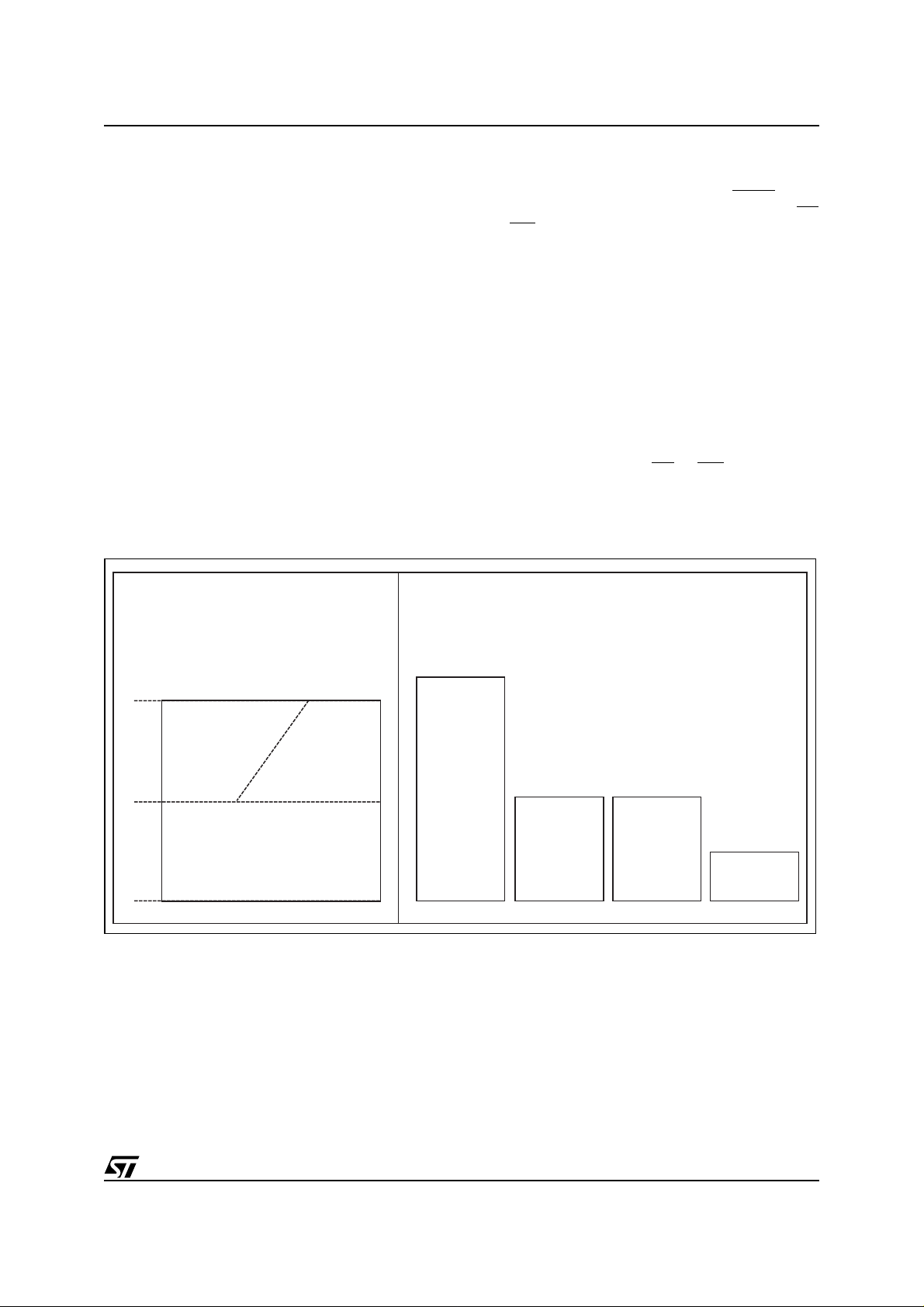
Figure 7. Comparison of uPSD33xx with Standard 8032 Performance
1-byte, 1-Cycle Instructions
Instruction A Instruction B Instruction C
Turbo uPSD33XX
Execute Instruction and
Pre-Fetch Next Instruction
Execute Instruction and
Pre-Fetch Next Instruction
Execute Instruction and
Pre-Fetch Next Instruction
4 clocks (one machine cycle)
one machine cycle one machine cycle
MCU Clock
12 clocks (one machine cycle)
Instruction A
Standard 8032
Fetch Byte for Instruction A
Dummy Byte is Ignored (wasted bus access)
Turbo uPSD33XX executes instructions A, B, and C in the same
amount of time that a standard 8032 executes only instruction A.
Figure 8. Instruction Pre-Fetch Queue and Branch Cache
Branch 4
Code
Branch
Cache
(BC)
Branch 3
Code
Branch 2
Code
Branch 4
Code
Branch 3
Code
Branch 1
Code
Branch 4
Code
Branch 2
Code
Branch 1
Code
Branch 3
Code
Branch 2
Code
Branch 4
Code
Branch 3
Code
Branch 1
Code
Branch 4
Code
Branch 2
Code
Branch 1
Code
Branch 3
Code
Branch 2
Branch 4
Code
Code
Branch 1
Code
Execute Instruction A
and Fetch a Second Dummy Byte
Previous
Branch 4
Branch 3
Code
Branch 2
Code
Branch 1
Code
Previous
Branch 3
Previous
Branch 2
AI08808
Compare
Previous
Branch 1
Address
Program
Memory on
PSD Module
18/231
Instruction
Byte
8
Address
16
Wait
Load on Branch Address Match
6 Bytes of Instruction
Instruction Pre-Fetch Queue (PFQ)
Instruction
Byte
8
Address
16
Stall
Current
Branch
Address
8032
MCU
AI08809

uPSD33xx
Pre-Fetch Queue (PFQ) and Branch Cache
(BC)
The PFQ is always working to minimize the idle
bus time inherent to 8032 MCU architecture, to
eliminate wasted memory fetches, and to maximize memory bandwidth to the MCU. The PFQ
does this by running asynchronously in relation to
the MCU, looking ahead to pre-fetch code from
program memory during any idle bus periods. Only
necessary bytes will be fetched (no dumm y fe tches like standard 8032) . The PFQ w ill queue up t o
six code bytes in advance of execution, which significantly optimizes sequential program performance. However, when program execution
becomes non-sequential (program branch), a typical pre-fetch queue will empty itself and reload
new code, causing the MCU to stall. The Turbo
uPSD33xx diminishes this problem by using a
Branch Cache with the PFQ. The BC is a four-way,
fully associative cache, mea ning tha t when a program branch occurs, it's branch destination address is compared simultaneously with four recent
previous branch destinations stored in the BC.
Each of the four cache entries contain up to six
bytes of code related to a branch. If there is a hit
(a match), then all six code bytes of the matching
program branch are transferred immediate ly and
simultaneously from the BC to the PFQ, and execution on that branch continues with mini mal delay. This greatly reduces the chance that the MCU
will stall from an empty PFQ, and improves performance in embedded contro l systems where it is
quite common to branch and loop in relatively
small code localities.
By default, the PFQ and BC are enabled after
power-up or reset. The 8032 can disable the PFQ
and BC at runtime if desired by writing to a specific
SFR (BUSCON).
The memory in the PSD module operates with
variable wait states depending on the value spec ified in the SFR named BUSCON. For example, a
5V uPSD33xx device operating at a 40MHz crystal
frequency requires four memory wait states (equal
to four MCU clocks). In this example, once the
PFQ has one or more bytes of code, the wait
states become transparent and a full 10 MIPS is
achieved when the program stream consists of sequential one-byte, one machine-cycle instructions
as shown in Figure 7., page 18 (transparent because a machine-cycle is four MCU clocks which
equals the memory pre-fetch wait time that is also
four MCU clocks). But it is als o important to understand PFQ operation on multi -cycle instructions.
PFQ Example, Multi-cycle Instructions
Let us look at a string of two-byte, two-cycle instructions in Figure 9., page 20. There are three
instructions executed sequentially in this example,
instructions A, B, and C. Each of the time divisions
in the figure is one machine-c ycle of four clocks,
and there are six phases to reference in this discussion. Each instruction is pre-fetched into the
PFQ in advance of execution by the MCU. Prior to
Phase 1, the PFQ has pre-fetched the two instruction bytes (A1 and A2) of instruction A. During
Phase one, both byte s are loaded into the MCU
execution unit. Also in Phase 1 , the PFQ is prefetching the first byte (B1) of instruction B from
program memory. In Phase 2, the MCU is processing Instruction A internally while the PF Q is
pre-fetching the second byte (B2) of Instruction B.
In Phase 3, both bytes of instru ction B are loa ded
into the MCU execution uni t and the PFQ b egins
to pre-fetch bytes for the third instruction C. In
Phase 4 Instruction B is processed and the prefetching con ti n u es , eliminating i dle bu s cycles and
feeding a continuous flow of operands and opcodes to t he MCU execution un it.
The uPSD33xx MCU instructions are an exact 1/3
scale of all standard 8032 instructions with regard
to number of cycles per instruction. Figure
10., page 20 shows the e quivalent instruction se-
quence from the example above on a standard
8032 for comparison.
Aggregate Perform ance
The stream of two-byte, two-cycle instructions in
Figure 9., page 20, running on a 40MHz, 5V,
uPSD33xx will yield 5 MIPs. And we saw the
stream of one-byte, one-cycle instructions in Fig-
ure 7., page 18, on the sam e M CU yield 10 MIP s.
Effective performance will depend on a number of
things: the MCU clock frequency; the mixture of instructions types (bytes and cycles) in the application; the amount of time an empty PFQ stalls the
MCU (mix of instruction types and misses on
Branch Cache); and the operating vol tage. A 5V
uPSD33xx device operates with four memory wait
states, but a 3.3V de vice operat es wi th five mem ory wait states yielding 8 MIPS peak com pared t o
10 MIPs peak for 5V device. The same number of
wait states will apply to both program f etches and
to data READ/WRITEs unless otherwise specified
in the SFR named BUSCON.
In general, a 3X aggregate performance increase
is expected over any standard 8032 application
running at the same clock frequency.
19/231

uPSD33xx
Figure 9. PFQ Operation on Multi-cycl e Instruction s
Three 2-byte, 2-cycle Instructions on uPSD33XX
Pre-Fetch Inst A Pre-Fetch Inst B Pre-Fetch Inst C
PFQ
Inst A, Byte 1
4-clock
Macine Cycle
Inst A, Byte 2 Inst B, Byte 1 Inst B, Byte 2 Inst C, Byte 1 Inst C, Byte 2
Continue to Pre-Fetch
Phase 1 Phase 2 Phase 3 Phase 4 Phase 6Phase 5
MCU
Previous Instruction A1 A2 Process A B1 B2 Process B C1 C2
Execution
Instruction A Instruction B Instruction C
Figure 10. uPSD33xx Multi-cycle Instructions Compared to Standard 8032
Three 2-byte, 2-cycle Instructions, uPSD33XX vs. Standard 8032
24 Clocks Total (4 clocks per cycle)
uPSD33XX
Std 8032
A1
Byte 1
A2
Inst A
Byte 2
B1
1 Cycle
Process Inst A
B2
1 Cycle
Inst B
C1
C2
Inst C
72 Clocks (12 clocks per cycle)
Byte 1
Byte 2
Process Inst B
Byte 1
Byte 2
Process C
Process Inst C
Next Inst
AI08810
AI08811
20/231

MCU MODU LE DISCRIPTION
This section provides a detail description of the
MCU Module system functions and peripherals, including:
■ 8032 MCU Registers
■ Special Function Registers
■ 8032 Addressing Modes
■ uPSD33xx Instruction Set Summary
■ Dua l Data Po i nters
■ Debug Unit
■ Interrupt System
■ MCU Clock Generation
■ Power Saving Modes
■ Oscillator and Ext ernal C om ponents
8032 MCU REGISTERS
The uPSD33xx has the following 8 032 MCU core
registers, also shown in Figure 11.
Figure 11. 8032 MCU Registers
A
B
SP
PCH
DPTR(DPH)
AI06636
PCL
PSW
R0-R7
DPTR(DPL)
Stack Pointer (SP)
The SP is an 8-bit register which holds the current
location of the top of th e stack. It is incremented
before a value is pushed ont o t he st ack , and dec remented after a value is popped off the stack. The
SP is initialized to 07h after reset. This causes the
stack to begin at locat ion 08h (top o f stack). To
avoid overlapping conflicts, the user must initialize
the top of the stack to 20h if all four banks of registers R0 - R7 are used, and the user must initialize
the top of stack to 30h if all of the 8032 bit memory
locations are used.
Data Pointer (DPTR)
DPTR is a 16-bit register consisting of two 8-bit
registers, DPL and DPH. The DPTR Register is
used as a base register to create an address for indirect jumps, table look-up operations, and for external data transfers (XDATA). When not used for
addressing, the DPTR Register can be used as a
general purpose 16-bit data register.
Accumulator
B Register
Stack Pointer
Program Counter
Program Status Word
General Purpose
Register (Bank0-3)
Data Pointer Register
uPSD33xx
■ I/O Ports
■ MCU Bus Interface
■ Supervisory Functions
■ Standard 8032 Timer/Counters
■ Serial UART Interf ac e s
■ IrDA Interface
2
■ I
C Interface
■ SPI Interface
■ Analog to Digital Converter
■ Programmable Counter Array (PCA)
Note: A full description of the 8032 instruction set
may be found in the uPSD33xx Programmers
Guide.
Very frequently, the DPTR Register is used to access XDATA using the External Direct addressing
mode. The uPSD33 xx has a specia l set of SFR
registers (DPTC, DPTM) to control a secondary
DPTR Register to speed memory-to-memory
XDATA transfers. Having dual DPTR Registers allows rapid switching between source and destination addresses (see details in DUAL DATA
POINTERS, page 37).
Program Counter (PC)
The PC is a 16-bit register consisting of two 8-bit
registers, PCL and PCH. This counter indicates
the address of the next instruction in program
memory to be fetched and executed. A reset forces the PC to location 0000h, which is where the reset jump vector is stored.
Accumulator (ACC)
This is an 8-bit general purpose register which
holds a source operand and rece ives the result of
arithmetic operations. The ACC Register can also
be the source or destination of logic and data
movement operations. For MUL and DIV instructions, ACC is combined with the B Register to hold
16-bit operands. The ACC is referred to as “A” in
the MCU instruction set.
B Register (B)
The B Register is a gene ra l purpo se 8-bit regi ster
for temporary data storage and also used as a 16bit register when concatenated with the ACC Register for use with MUL and DIV instructions.
21/231

uPSD33xx
General Purpose Registers (R0 - R7)
There are four banks of eight general purpose 8bit registers (R0 - R7), but only o ne bank of eight
registers is active at any given time dependin g on
the setting in the PSW word (described next). R0 R7 are generally used to assist in manipulating
values and moving data from one memory location
to another. These register banks physically reside
in the first 32 locations of 8032 internal DATA
SRAM, starting at address 00h. At reset, only the
first bank of eight registers is active (addresses
00h to 07h), and the stack begins at address 08h.
Program Stat us Wor d (PSW )
The PSW is an 8-bit regi ster wh ich st ores s everal
important bits, or flags, that are set and cleared by
many 8032 instructions, reflecting the current
state of the MCU core. Figure 12., page 22 shows
the individual flags.
Carry Flag (CY). This flag is set when the last
arithmetic operation that was executed results in a
carry (addition) or borrow (subtraction). It is
cleared by all other arithmetic operations. The CY
flag is also affected by Shift and Rotate Instructions.
Auxiliary Carry Flag (AC). This flag i s set when
the last arithmetic operation that was executed results in a carry into (addition) or borrow from (subtraction) the high-order nibble. It is cleared by all
other arithmetic operations.
General Purpose Flag (F0). This is a bit-addressable, general-purpose flag for use under software
control.
Register Bank Select Flags (RS1, RS0). These
bits select which ba nk of eight regist ers is used
during R0 - R7 register accesses (see Table 4)
Overflow Flag (OV). The OV flag is set when: an
ADD, ADDC, or SUBB instruction causes a sign
change; a MUL instruction results in an overflow
(result greater than 255); a DIV instruction causes
a divide-by-zero condition. The OV f lag is cl eared
by the ADD, ADDC, SUBB, MUL, and DIV instructions in all other cases. The CLRV instruction will
clear the OV flag at any time.
Parity Flag (P). The P flag is set if the sum of the
eight bits in the Accumulator is odd, and P is
cleared if the sum is even.
Table 4. .Register Bank Select Addresses
RS1 RS0
0 0 0 00h - 07h
0 1 1 08h - 0Fh
1 0 2 10h - 17h
1 1 3 18h - 1Fh
Register
Bank
8032 Internal
DATA Address
Figure 12. Program Statu s W or d (PS W ) Re gi st er
MSB
CY
PSW
Carry Flag
Auxillary Carry Flag
General Purpose Flag
AC FO RS1 RS0 OV P
Register Bank Select Flags
(to select Bank0-3)
LSB
Reset Value 00h
Parity Flag
Bit not assigned
Overflow Flag
AI06639
22/231

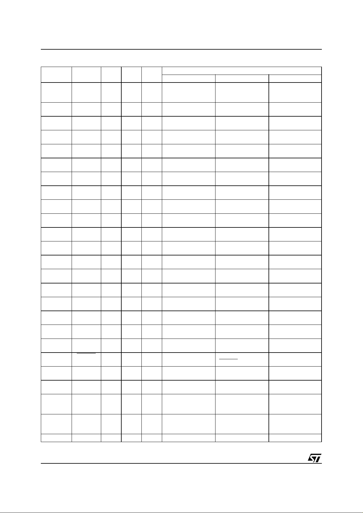
SPECIA L FUNCTION REGISTER S (SFR)
A group of registers designated as Special Function Register (SFR) is shown in Table 5., page 24.
SFRs control the operating modes of the MCU
core and also control the peripheral interfaces and
I/O pins on the MCU Module. The SFRs can be accessed only by using the Direct Addressing method within the address range from 80h t o FFh of
internal 8032 SRAM. Sixteen addresses in SFR
address space are both byte- and bit-addressable.
The bit-addressable SFRs are noted in Table 5.
86 of a possible 128 SFR addresses are occupied.
The remaining unoccupied SFR addresses (designated as “RESERVED” in Table 5) should not be
written. Reading unoccupied lo cations will return
an undefined value.
Note: There is a separate set of control registers
for the PSD Module, designated as csiop, and they
are described in the PSD MODULE, page 133.
The I/O pins, PLD, and other functions on the PSD
Module are NOT controlled by SFRs.
SFRs are categorized as follows:
■ MCU core registers:
IP, A, B, PSW, SP, DPTL, DPTH, DPTC,
DPTM
■ MCU Module I/O Port registers:
P1, P3, P4, P1SFS0, P1SFS1, P3SFS,
P4SFS0, P4SFS 1
■ Standard 8032 Timer reg isters
TCON, TMOD, T2CON, TH0, TH1, TH2, TL0,
TL1, TL2, RCAP2L, RCAP2H
■ Standard Serial Interfaces (UART)
uPSD33xx
SCON0, SBUF0, SCON1, SBUF1
■ Power, clock, and bus timi ng regis ters
PCO N, CCON0, B U SCON
■ Hardware wat ch do g t imer re gist ers
WDKEY, WDRST
■ Interrupt system registers
IP, I PA, IE, IEA
■ Prog. Coun te r Array ( P CA ) cont ro l
registers
PCACL0, PCACH0, PCACON0, PCASTA,
PCACL1, PCACH1, PCACON1, CCON2,
CCON3
■ PCA capture/compare and PWM regist ers
CAPCOML0, CAPCOMH0, TCMMODE0,
CAPCOML1, CAPCOMH1, TCMMODE2,
CAPCOML2, CAPCOMH2, TCMMODE2,
CAPCOML3, CAPCOMH3, TCMMODE3,
CAPCOML4, CAPCOMH4, TCMMODE4,
CAPCOML5, CAPCOMH5, TCMMODE5,
PWMF0, PMWF1
■ SPI interface registers
SPICLKD, SPISTAT, SPITDR, SPIRDR,
SPICON0, SPICON1
2
■ I
C interface registers
S1SETUP, S1CON, S1STA, S1 D AT , S1ADR
■ Analog to Digital Converter registers
ACON, ADCPS, ADAT0, ADAT1
■ IrDA interface register
IRDACON
23/231
uPSD33xx
Table 5. SFR Memory Map with Direct Address and Reset Value
SFR
Addr
(hex)
80 RESERVED
81 SP SP[7:0] 07
82 DPL DPL[7:0] 00 Data
83 DPH DPH[7:0] 00
84 RESERVED
85 DPTC – AT – – – DPSEL[2:0] 00
86 DPTM – – – – MD1[1:0] MD0[1:0] 00
87 PCON SMOD0 SMOD1 – POR RCLK1 TCLK1 PD IDLE 00
88
89 TMOD GATE C/T
8A TL0 TL0[7:0] 00
8B TL1 TL1[7:0] 00
8C TH0 TH0[7:0] 00
8D TH1 TH1[7:0] 00
8E P1SFS0 P1SFS0[7:0] 00
8F P1SFS1 P1SFS1[7:0] 00
90
91 P3SFS P3SFS[7:0] 00
92 P4SFS0 P4SFS0[7:0] 00
93 P4SFS1 P4SFS1[7:0] 00
(1)
(1)
SFR
Name
TCON
P1
76 5 43210
TF1
<8Fh>
P1.7
<97h>
TR1
<8Eh>
P1.6
<96h>
Bit Name and <Bit Address> Reset
Value
(hex)
TF0
<8Dh>
M1 M0 GATE C/T M1 M0 00
P1.5
<95h>
TR0
<8Ch>
P1.4
<94h>
IE1
<8Bh>
P1.3
<93h>
IT1
<8Ah>
P1.2
<92h>
IE0
<89h>
P1.1
<91h>
IT0
<88h>
P1.0
<90h>
00
FF
with Link
Pointer
(SP), page
Pointer
(DPTR), p
age 21
13., page
14., page
24., page
39., page
40., page
Standard
SFRs, pag
29., page
30., page
25., page
28., page
32., page
33., page
Reg.
Descr.
Stack
21
Table
37
Table
38
Table
50
Table
70
Table
72
Timer
e69
Table
60
Table
60
Table
57
Table
60
Table
61
Table
61
24/231

uPSD33xx
SFR
Addr
(hex)
94 ADCPS – – – – ADCCE ADCPS[2:0] 00
95 ADAT0 ADATA[7:0] 00
96 ADAT1 – – – – – – ADATA[9:8] 00
97 ACON AINTF AINTEN ADEN ADS[2:0] ADST ADSF 00
98
99 SBUF0 SBUF0[7:0] 00
9A RESERVED
9B RESERVED
9C RESERVED
9D BUSCON EPFQ EBC WRW1 WRW0 RDW1 RDW0 CW1 CW0 EB
9E RESERVED
9F RESERVED
A0 RESERVED
A1 RESERVED
A2 PCACL0 PCACL0[7:0] 00
A3 PCACH0 PCACH0[7:0] 00
A4 PCACON0 EN_ALL EN_PCA EOVF1 PCA_IDL – – CLK_SEL[1:0] 00
A5 PCASTA OVF1 INTF5 INTF4 INTF3 OVF0 INTF2 INTF1 INTF0 00
A6 WDTRST WDTRST[7:0] 00
A7 IEA EADC ESPI EPCA ES1 – – EI2C – 00
(1)
SFR
Name
SCON0
76 5 43210
SM0
<9Fh>
SM1
<9Eh>
Bit Name and <Bit Address> Reset
SM2
<9Dh>
REN
<9Ch>
TB8
<9Bh>
RB8
<9Ah>TI<99h>RI<9h8>
Value
(hex)
00
Reg.
Descr.
with Link
Table
64., page
122
Table
65., page
122
Table
66., page
122
Table
63., page
121
Table
45., page
82
Figure
25., page
79
Table
35., page
63
Table
67., page
124
Table
67., page
124
Table
70., page
129
Table
72., page
131
Table
38., page
68
Table
18., page
44
25/231

uPSD33xx
SFR
Addr
(hex)
(1)
A8
A9
AA
AB
AC
AD
SFR
Name
IE
TCMMODE
0
TCMMODE
1
TCMMODE
2
CAPCOML
0
CAPCOMH
0
76 5 43210
EA
<AFh>
–
EINTF E_COMP CAP_PE CAP_NE MATCH TOGGLE PWM[1:0] 00
EINTF E_COMP CAP_PE CAP_NE MATCH TOGGLE PWM[1:0] 00
EINTF E_COMP CAP_PE CAP_NE MATCH TOGGLE PWM[1:0] 00
Bit Name and <Bit Address> Reset
Value
(hex)
ET2
<ADh>
ES0
<ACh>
ET1
<ABh>
EX1
<AAh>
ET0
<A9h>
EX0
<A8h>
CAPCOML0[7:0] 00
CAPCOMH0[7:0] 00
00
Reg.
Descr.
with Link
Table
17., page
43
Table
73., page
132
Table
67., page
124
Table
AE WDTKEY WDTKEY[7:0] 55
37., page
68
AF
B0
(1)
B1
B2
B3
CAPCOML
1
P3
CAPCOMH
1
CAPCOML
2
CAPCOMH
2
P3.7
<B7h>
P3.6
<B6h>
P3.5
<B5h>
CAPCOML1[7:0] 00
P3.4
<B4h>
P3.3
<B3h>
P3.2
<B2h>
P3.1
<B1h>
P3.0
<B0h>
FF
CAPCOMH1[7:0] 00
CAPCOML2[7:0] 00
CAPCOMH2[7:0] 00
Table
67., page
124
Table
26., page
58
Table
67., page
124
B4 PWMF0 PWMF0[7:0] 00
B5 RESERVED
B6 RESERVED
Table
B7 IPA PADC PSPI PPCA PS1 – – PI2C – 00
20., page
45
Table
19., page
44
B8
(1)
IP – –
PT2
<BDh>
PS0
<BCh>
PT1
<BBh>
PX1
<BAh>
PT0
<B9h>
PX0
<B8h>
00
B9 RESERVED
BA PCACL1 PCACL1[7:0] 00 Table
BB PCACH1 PCACH1[7:0] 00
67., page
124
Table
BC PCACON1 – EN_PCA EOVF1 PCA_IDL – – CLK_SEL[1:0] 00
71., page
130
26/231

uPSD33xx
SFR
Addr
(hex)
BD
BE
BF
(1)
C0
C1
C2
C3
C4
C5
C6
SFR
Name
TCMMODE
3
TCMMODE
4
TCMMODE
5
P4
CAPCOML
3
CAPCOMH
3
CAPCOML
4
CAPCOMH
4
CAPCOML
5
CAPCOMH
5
76 5 43210
EINTF E_COMP CAP_PE CAP_NE MATCH TOGGLE PWM[1:0] 00
EINTF E_COMP CAP_PE CAP_NE MATCH TOGGLE PWM[1:0] 00
EINTF E_COMP CAP_PE CAP_NE MATCH TOGGLE PWM[1:0] 00
P4.7
<C7h>
P4.6
<C6h>
Bit Name and <Bit Address> Reset
P4.5
<C5h>
P4.4
<C4h>
P4.3
<C3h>
P4.2
<C2h>
P4.1
<C1h>
P4.0
<C0h>
CAPCOML3[7:0] 00
CAPCOMH3[7:0] 00
CAPCOML4[7:0] 00
CAPCOMH4[7:0] 00
CAPCOML5[7:0] 00
CAPCOMH5[7:0] 00
C7 PWMF1 PWMF1[7:0] 00
CP/
RL2
<C8h>
C8
(1)
T2CON
TF2
<CFh>
EXF2
<CEh>
RCLK
<CDh>
TCLK
<CCh>
EXEN2
<CBh>
TR2
<CAh>
C/T2
<C9h>
C9 RESERVED
CA RCAP2L RCAP2L[7:0] 00
CB RCAP2H RCAP2H[7:0] 00
CC TL2 TL2[7:0] 00
CD TH2 TH2[7:0] 00
CE IRDACON – IRDA_EN BIT_PULS CDIV4 CDIV3 CDIV2 CDIV1 CDIV0 0F
D0
(1)
PSW
CY
<D7h>AC<D6h>F0<D5h>
RS[1:0]
<D4h, D3h>
OV
<D2h>
–
P
<D0>
D1 RESERVED
D2 SPICLKD SPICLKD[5:0] – – 04
D3 SPISTAT – – – BUSY TEISF RORISF TISF RISF 02
Value
(hex)
FF
00
00
Reg.
Descr.
with Link
Table
73., page
132
Table
27., page
58
Table
67., page
124
Table
41., page
75
Standard
Timer
SFRs, pag
e69
Table
48., page
93
Program
Status
Word
(PSW), pa
ge 22
Table
61., page
118
Table
62., page
119
27/231
uPSD33xx
SFR
Addr
(hex)
SFR
Name
76 5 43210
Bit Name and <Bit Address> Reset
Value
(hex)
Reg.
Descr.
with Link
D4 SPITDR SPITDR[7:0] 00 Table
62., page
D5 SPIRDR SPIRDR[7:0] 00
119
Table
D6 SPICON0 – TE RE SPIEN SSEL FLSB SPO – 00
59., page
117
Table
D7 SPICON1 – – – – TEIE RORIE TIE RIE 00
60., page
118
Table
46., page
D8
(1)
SCON1
SM0
<DF
SM1
<DE>
SM2
<DD>
REN
<DC>
TB8
<DB>
RB8
<DA>TI<D9>RI<D8>
00
Figure
D9 SBUF1 SBUF1[7:0] 00
25., page
DA RESERVED
Table
DB S1SETUP SS_EN SMPL_SET[6:0] 00
55., page
105
Table
DC S1CON CR2 EN1 STA STO ADDR AA CR1 CR0 00
50., page
100
Table
DD S1STA GC STOP INTR TX_MD B_BUSY B_LOST ACK_R
SLV 00
52., page
103
Table
DE S1DAT S1DAT[7:0] 00
53., page
104
Table
DF S1ADR S1ADR[7:0] 00
54., page
104
Accumulat
E0
(1)
A
<bit addresses: E7h, E6h, E5h, E4h, E3h, E2h, E1h, E0h>
A[7:0]
00
(ACC), pa
ge 21
E1
to
RESERVED
EF
F0
(1)
B
<bit addresses: F7h, F6h, F5h, F4h, F3h, F2h, F1h, F0h>
B[7:0]
00
B Register
(B), page
F1 RESERVED
F2 RESERVED
F3 RESERVED
F4 RESERVED
F5 RESERVED
F6 RESERVED
83
79
or
21
28/231
uPSD33xx
SFR
Addr
(hex)
F7 RESERVED
F8 RESERVED
F9 CCON0 – – – DBGCE CPU_AR CPUPS[2:0] 10
FA RESERVED
FB CCON2 – – – PCA0CE PCA0PS[3:0] 10
FC CCON3 – – – PCA1CE PCA1PS[3:0] 10
FD RESERVED
FE RESERVED
FF RESERVED
Note: 1. This SFR can be addressed by i ndividual bits (Bit Addr ess mode) or addressed by the entire by te (Direct Address mode) .
SFR
Name
76 5 43210
Bit Name and <Bit Address> Reset
Value
(hex)
with Link
21., page
68., page
69., page
Reg.
Descr.
Table
47
Table
125
Table
125
29/231

uPSD33xx
8032 ADDRESSING MODES
The 8032 MCU uses 11 different addressing
modes listed below:
■ Register
■ Direct
■ Register Indirect
■ Immediate
■ External Direct
■ External Indirect
■ Indexed
■ Relative
■ Absolute
■ Long
■ Bit
Register Addressing
This mode uses the con tents of one of the registers R0 - R7 (selected by the last three bits in the
instruction opcode) as the operand source or destination. This mode is very efficient since an additional instruction byte is not needed to ident ify the
operand. For example:
MOV A, R7 ; Move contents of R7 to accumulator
Direct Addressing
This mode uses an 8-bit address, which is contained in the second byte of the instruction, to directly address an operand which reside s in either
8032 DATA SRAM (internal address range 00h07Fh) or resides in 8032 SFR (internal address
range 80h-FFh). This m ode is quite fast sin ce the
range limit is 256 bytes of internal 8032 SRAM.
For example:
MOV A, 40h ; Move contents of DATA SRAM
; at location 40h into the accumulator
Register Indirect Addressing
This mode uses an 8-bit address contained in either Register R0 or R1 to indirectly address an operand which resides in 8032 IDATA SRAM
(internal address range 80h-FFh). Although 8 032
SFR registers also occupy the same physical address range as IDATA, SFRs will not be accessed
by Register Indirect mode. S F Rs m ay on ly be accesses using Direct address mode. For example:
MOV A, @R0 ; Move into the accumulator the
; contents of IDATA SRAM that is
; pointed to by the address
; contained in R0.
Imm ediate Addressing
This mode uses 8-bits of dat a (a constant) contained in the second byte of the instruction, and
stores it into the memory location or register indicated by the first byte of the in struction. Thu s, the
data is immediately available within the instruction.
This mode is commonly used to initialize registers
and SFRs or to perform mask operations.
There is also a 16-bit version of this mode for loading the DPTR Register. In this case, the two bytes
following the instruction byte contain the 16-bit value. For example:
MOV A, 40# ; Move the constant, 40h, into
; the accumulator
MOV DPTR, 1234# ; Move the constant, 1234h, into
; DPTR
External Direct Addressing
This mode will access external me mory (XDATA)
by using the 1 6-bit address stored in the DPTR
Register. There are only two instructions using this
mode and both use the accumulator to either receive a byte from external memory addressed by
DPTR or to send a byte from the accumul ator to
the address in DPTR. The uPSD 33xx has a special feature to alternate the contents (source and
destination) of DPTR rapidly to implement very efficient memory-to-memory transfers. For example:
MOVX A, @DPTR ; Move contents of accumulator to
; XDATA at address contained in
; DPTR
MOVX @DPTR, A ; Move XDATA to accumulator
Note: See details in DUAL DATA
POINTERS, page 37.
External Indirect Addressing
This mode will access external me mory (XDATA)
by using the 8-bit address stored in either Register
R0 or R1. This is the fastest way to access XDATA
(least bus cycles), but because only 8-bits are
available for address, this mode limits XDATA to a
size of only 256 bytes (the traditional Port 2 of the
8032 MCU is not available in the uPSD33xx, so it
is not possible to write the upper address byte).
This mode is not supported by uPSD33xx.
For example:
MOVX @R0,A ; Move into the accumulator the
; XDATA that is pointed to by
; the address contained in R0.
30/231
 Loading...