


Flash Program mable System Devices
with 8032 Microcontroller Core and 64 Kbit SRAM
FEAT URES SUM MARY
■ FAST 8-BIT 8032 MCU
– 40MHz at 5.0V, 24MHz at 3.3V
– Core, 12-clocks per instruction
■ DUAL FLASH MEMORIES WITH MEMORY
MANAGEMENT
– Place either memory into 8032 program
address space or data address space
– READ-while-WRITE operation for In-
Application Programming and EEPR OM
emulation
– Single voltage program and erase
– 100K minimum erase cycl e s, 1 5 -ye a r
retention
■ CLOCK, RESET, AND SUPPLY
MANAGEMENT
– SRAM is Battery Backup capable
– Normal, Idle, and Power Down Modes
– Power-on and Low Voltage reset
supervisor
– Programmable Watchdog Timer
■ PROGRAMMABLE LOGIC, GENERAL
PURPOSE
– 16 macrocells
– Implements state machines, glue-logic,
and so forth
■ COMMUNICATION INTERFACES
– USB v1.1, low-speed 1.5Mbps, 3
endpoints
2
C Master/Slave bus controller
–I
– Two UARTs with independent baud rate
– Six I/O ports with up to 46 I/O pins
– 8032 Address/Data bus available on
TQFP80 packa ge
– 5 PWM outputs, 8-bit resolution
■ JTAG IN-SYSTEM PROG RAMMING
– Program the entire device in as little as
10 seconds
uPSD3234A, uPSD3234BV
uPSD3233B, uPSD3233BV
Figure 1. Packages
TQFP52 (T)
52-lead, Thin,
Quad Flat
TQFP80 (U)
80-lead, Thin,
Qual Flat
■ A/D CONVERTER
– Four channels, 8-bit resolution, 10µs
■ TIMERS AND INTERRUPTS
– Three 8032 standard 16-bit timers
– 10 Interrupt sources with two external
interrupt pins
■ Single Supply Voltage
– 4.5 to 5.5V
– 3.0 to 3.6V
1/170November 2004

uPSD3234A, uPSD3234BV, uPSD3233B, uPSD3233BV
Table 1. Device Summary
Max
Part Number
uPSD3233B-40T6 40 128K 32K 8K 37 No No 4.5-5.5 TQFP52 –40°C to 85°C
uPSD3233BV-24T6 24 128K 32K 8K 37 No No 3.0-3.6 TQFP52 –40°C to 85°C
uPSD3233B-40U6 40 128K 32K 8K 46 No Yes 4.5-5.5 TQFP80 –40°C to 85°C
uPSD3233BV-24U6 24 128K 32K 8K 46 No Yes 3.0-3.6 TQFP80 –40°C to 85°C
uPSD3234A-40T6 40 256K 32K 8K 37 Yes No 4.5-5.5 TQFP52 –40°C to 85°C
uPSD3234A-40U6 40 256K 32K 8K 46 Yes Yes 4.5-5.5 TQFP80 –40°C to 85°C
uPSD3234BV-24U6 24 256K 32K 8K 46 No Yes 3.0-3.6 TQFP80 –40°C to 85°C
Clock
(MHz)
1st
Flash
(bytes)
2nd
Flash
(bytes)
SRAM
(bytes)
GPIO USB
8032
Bus
V
(V)
CC
Pkg. Temp.
2/170

uPSD3234A, uPSD3234BV, uPSD3233B, uPSD3233BV
TABLE OF CONTENTS
FEATURES SUMMARY . . . . . . . . . . . . . . . . . . . . . . . . . . . . . . . . . . . . . . . . . . . . . . . . . . . . . . . . . . . . . 1
SUMMARY DESCRIPTION. . . . . . . . . . . . . . . . . . . . . . . . . . . . . . . . . . . . . . . . . . . . . . . . . . . . . . . . . . . 7
52-PIN PACKAGE I/O PORT . . . . . . . . . . . . . . . . . . . . . . . . . . . . . . . . . . . . . . . . . . . . . . . . . . . . . . . . 12
ARCHITECTURE OVERVIEW . . . . . . . . . . . . . . . . . . . . . . . . . . . . . . . . . . . . . . . . . . . . . . . . . . . . . . . 13
Memory Organization . . . . . . . . . . . . . . . . . . . . . . . . . . . . . . . . . . . . . . . . . . . . . . . . . . . . . . . . . . 13
Registers . . . . . . . . . . . . . . . . . . . . . . . . . . . . . . . . . . . . . . . . . . . . . . . . . . . . . . . . . . . . . . . . . . . . 13
Program Memory. . . . . . . . . . . . . . . . . . . . . . . . . . . . . . . . . . . . . . . . . . . . . . . . . . . . . . . . . . . . . . 15
Data memory . . . . . . . . . . . . . . . . . . . . . . . . . . . . . . . . . . . . . . . . . . . . . . . . . . . . . . . . . . . . . . . . . 15
RAM . . . . . . . . . . . . . . . . . . . . . . . . . . . . . . . . . . . . . . . . . . . . . . . . . . . . . . . . . . . . . . . . . . . . . . . . 15
XRAM-DDC. . . . . . . . . . . . . . . . . . . . . . . . . . . . . . . . . . . . . . . . . . . . . . . . . . . . . . . . . . . . . . . . . . . 15
XRAM-PSD . . . . . . . . . . . . . . . . . . . . . . . . . . . . . . . . . . . . . . . . . . . . . . . . . . . . . . . . . . . . . . . . . . . 15
SFR . . . . . . . . . . . . . . . . . . . . . . . . . . . . . . . . . . . . . . . . . . . . . . . . . . . . . . . . . . . . . . . . . . . . . . . . . 16
Addressing Modes . . . . . . . . . . . . . . . . . . . . . . . . . . . . . . . . . . . . . . . . . . . . . . . . . . . . . . . . . . . . 16
Arithmetic Instructions. . . . . . . . . . . . . . . . . . . . . . . . . . . . . . . . . . . . . . . . . . . . . . . . . . . . . . . . . 17
Logical Instructions . . . . . . . . . . . . . . . . . . . . . . . . . . . . . . . . . . . . . . . . . . . . . . . . . . . . . . . . . . . 18
Data Transfers . . . . . . . . . . . . . . . . . . . . . . . . . . . . . . . . . . . . . . . . . . . . . . . . . . . . . . . . . . . . . . . . 20
Boolean Instructions. . . . . . . . . . . . . . . . . . . . . . . . . . . . . . . . . . . . . . . . . . . . . . . . . . . . . . . . . . . 23
Relative Offset . . . . . . . . . . . . . . . . . . . . . . . . . . . . . . . . . . . . . . . . . . . . . . . . . . . . . . . . . . . . . . . . 23
Jump Instructions . . . . . . . . . . . . . . . . . . . . . . . . . . . . . . . . . . . . . . . . . . . . . . . . . . . . . . . . . . . . . 24
Machine Cycles . . . . . . . . . . . . . . . . . . . . . . . . . . . . . . . . . . . . . . . . . . . . . . . . . . . . . . . . . . . . . . . 25
uPSD3200 HARDWARE DESCRIPTION . . . . . . . . . . . . . . . . . . . . . . . . . . . . . . . . . . . . . . . . . . . . . . . 27
MCU MODULE DISCRIPTION . . . . . . . . . . . . . . . . . . . . . . . . . . . . . . . . . . . . . . . . . . . . . . . . . . . . . . . 28
Special Function Registers . . . . . . . . . . . . . . . . . . . . . . . . . . . . . . . . . . . . . . . . . . . . . . . . . . . . . 28
INTERRUPT SYSTEM. . . . . . . . . . . . . . . . . . . . . . . . . . . . . . . . . . . . . . . . . . . . . . . . . . . . . . . . . . . . . . 35
External Int0. . . . . . . . . . . . . . . . . . . . . . . . . . . . . . . . . . . . . . . . . . . . . . . . . . . . . . . . . . . . . . . . . . 35
Timer 0 and 1 Interrupts . . . . . . . . . . . . . . . . . . . . . . . . . . . . . . . . . . . . . . . . . . . . . . . . . . . . . . . . 35
Timer 2 Interrupt . . . . . . . . . . . . . . . . . . . . . . . . . . . . . . . . . . . . . . . . . . . . . . . . . . . . . . . . . . . . . . 35
2
I
C Interrupt . . . . . . . . . . . . . . . . . . . . . . . . . . . . . . . . . . . . . . . . . . . . . . . . . . . . . . . . . . . . . . . . . . 35
External Int1. . . . . . . . . . . . . . . . . . . . . . . . . . . . . . . . . . . . . . . . . . . . . . . . . . . . . . . . . . . . . . . . . . 35
DDC Interrupt . . . . . . . . . . . . . . . . . . . . . . . . . . . . . . . . . . . . . . . . . . . . . . . . . . . . . . . . . . . . . . . . . 35
USB Interrupt. . . . . . . . . . . . . . . . . . . . . . . . . . . . . . . . . . . . . . . . . . . . . . . . . . . . . . . . . . . . . . . . . 35
USART Interrupt . . . . . . . . . . . . . . . . . . . . . . . . . . . . . . . . . . . . . . . . . . . . . . . . . . . . . . . . . . . . . . 36
Interrupt Priority Structure. . . . . . . . . . . . . . . . . . . . . . . . . . . . . . . . . . . . . . . . . . . . . . . . . . . . . . 3 7
Interrupts Enable Structure . . . . . . . . . . . . . . . . . . . . . . . . . . . . . . . . . . . . . . . . . . . . . . . . . . . . . 37
How Interrupts are Handled . . . . . . . . . . . . . . . . . . . . . . . . . . . . . . . . . . . . . . . . . . . . . . . . . . . . . 39
POWER-SAVING MODE. . . . . . . . . . . . . . . . . . . . . . . . . . . . . . . . . . . . . . . . . . . . . . . . . . . . . . . . . . . . 40
Idle Mode . . . . . . . . . . . . . . . . . . . . . . . . . . . . . . . . . . . . . . . . . . . . . . . . . . . . . . . . . . . . . . . . . . . . 40
3/170

uPSD3234A, uPSD3234BV, uPSD3233B, uPSD3233BV
Power-Down Mode . . . . . . . . . . . . . . . . . . . . . . . . . . . . . . . . . . . . . . . . . . . . . . . . . . . . . . . . . . . . 40
Power Control Register. . . . . . . . . . . . . . . . . . . . . . . . . . . . . . . . . . . . . . . . . . . . . . . . . . . . . . . . . 4 0
Idle Mode . . . . . . . . . . . . . . . . . . . . . . . . . . . . . . . . . . . . . . . . . . . . . . . . . . . . . . . . . . . . . . . . . . . . 41
Power-Down Mode . . . . . . . . . . . . . . . . . . . . . . . . . . . . . . . . . . . . . . . . . . . . . . . . . . . . . . . . . . . . 41
I/O PORTS (MCU MODULE). . . . . . . . . . . . . . . . . . . . . . . . . . . . . . . . . . . . . . . . . . . . . . . . . . . . . . . . . 42
PORT Type and Description . . . . . . . . . . . . . . . . . . . . . . . . . . . . . . . . . . . . . . . . . . . . . . . . . . . . . 43
OSCILLATOR . . . . . . . . . . . . . . . . . . . . . . . . . . . . . . . . . . . . . . . . . . . . . . . . . . . . . . . . . . . . . . . . . . . . 45
SUPERVISORY. . . . . . . . . . . . . . . . . . . . . . . . . . . . . . . . . . . . . . . . . . . . . . . . . . . . . . . . . . . . . . . . . . . 45
External Reset . . . . . . . . . . . . . . . . . . . . . . . . . . . . . . . . . . . . . . . . . . . . . . . . . . . . . . . . . . . . . . . . 46
Low VDD Voltage Reset . . . . . . . . . . . . . . . . . . . . . . . . . . . . . . . . . . . . . . . . . . . . . . . . . . . . . . . . 4 6
Watchdog Timer Overflow . . . . . . . . . . . . . . . . . . . . . . . . . . . . . . . . . . . . . . . . . . . . . . . . . . . . . . 46
USB Reset . . . . . . . . . . . . . . . . . . . . . . . . . . . . . . . . . . . . . . . . . . . . . . . . . . . . . . . . . . . . . . . . . . . 46
WATCHDOG TIMER. . . . . . . . . . . . . . . . . . . . . . . . . . . . . . . . . . . . . . . . . . . . . . . . . . . . . . . . . . . . . . . 47
TIMER/COUNTERS (TIMER 0, TIMER 1 AND TIMER 2). . . . . . . . . . . . . . . . . . . . . . . . . . . . . . . . . . . 49
Timer 0 and Timer 1. . . . . . . . . . . . . . . . . . . . . . . . . . . . . . . . . . . . . . . . . . . . . . . . . . . . . . . . . . . . 49
Timer 2 . . . . . . . . . . . . . . . . . . . . . . . . . . . . . . . . . . . . . . . . . . . . . . . . . . . . . . . . . . . . . . . . . . . . . . 53
STANDARD SERIAL INTERFACE (UART) . . . . . . . . . . . . . . . . . . . . . . . . . . . . . . . . . . . . . . . . . . . . . 56
Multiprocessor Comm u ni cations. . . . . . . . . . . . . . . . . . . . . . . . . . . . . . . . . . . . . . . . . . . . . . . . . 56
Serial Port Control Register . . . . . . . . . . . . . . . . . . . . . . . . . . . . . . . . . . . . . . . . . . . . . . . . . . . . . 56
ANALOG-TO-DIGITAL CONVERTOR (ADC) . . . . . . . . . . . . . . . . . . . . . . . . . . . . . . . . . . . . . . . . . . . 65
ADC Interrupt . . . . . . . . . . . . . . . . . . . . . . . . . . . . . . . . . . . . . . . . . . . . . . . . . . . . . . . . . . . . . . . . . 65
PULSE WIDTH MODULATION (PWM). . . . . . . . . . . . . . . . . . . . . . . . . . . . . . . . . . . . . . . . . . . . . . . . . 67
4-channel PWM Unit (PWM 0-3) . . . . . . . . . . . . . . . . . . . . . . . . . . . . . . . . . . . . . . . . . . . . . . . . . .67
Programmable Period 8-bit PWM. . . . . . . . . . . . . . . . . . . . . . . . . . . . . . . . . . . . . . . . . . . . . . . . . 69
PWM 4 Channel Operation . . . . . . . . . . . . . . . . . . . . . . . . . . . . . . . . . . . . . . . . . . . . . . . . . . . . . . 7 0
2
I
C INTERFACE . . . . . . . . . . . . . . . . . . . . . . . . . . . . . . . . . . . . . . . . . . . . . . . . . . . . . . . . . . . . . . . . . . 71
Serial Status Register (SxSTA: S1STA, S2STA). . . . . . . . . . . . . . . . . . . . . . . . . . . . . . . . . . . . . 73
Data Shift Register (SxDAT: S1DAT, S2DAT) . . . . . . . . . . . . . . . . . . . . . . . . . . . . . . . . . . . . . . . 73
Address Register (SxADR: S1ADR, S2ADR). . . . . . . . . . . . . . . . . . . . . . . . . . . . . . . . . . . . . . . . 74
DDC INTERFACE . . . . . . . . . . . . . . . . . . . . . . . . . . . . . . . . . . . . . . . . . . . . . . . . . . . . . . . . . . . . . . . . . 75
Special Function Register for the DDC Interface . . . . . . . . . . . . . . . . . . . . . . . . . . . . . . . . . . . . 76
Host Type Detection . . . . . . . . . . . . . . . . . . . . . . . . . . . . . . . . . . . . . . . . . . . . . . . . . . . . . . . . . . . 79
DDC1 Protocol. . . . . . . . . . . . . . . . . . . . . . . . . . . . . . . . . . . . . . . . . . . . . . . . . . . . . . . . . . . . . . . . 80
DDC2B Protocol. . . . . . . . . . . . . . . . . . . . . . . . . . . . . . . . . . . . . . . . . . . . . . . . . . . . . . . . . . . . . . . 81
USB HARDWARE. . . . . . . . . . . . . . . . . . . . . . . . . . . . . . . . . . . . . . . . . . . . . . . . . . . . . . . . . . . . . . . . . 82
4/170

uPSD3234A, uPSD3234BV, uPSD3233B, uPSD3233BV
USB related registers . . . . . . . . . . . . . . . . . . . . . . . . . . . . . . . . . . . . . . . . . . . . . . . . . . . . . . . . . . 82
Transceiver . . . . . . . . . . . . . . . . . . . . . . . . . . . . . . . . . . . . . . . . . . . . . . . . . . . . . . . . . . . . . . . . . . 89
Receiver Characteristics. . . . . . . . . . . . . . . . . . . . . . . . . . . . . . . . . . . . . . . . . . . . . . . . . . . . . . . . 90
External USB Pull-Up Resistor. . . . . . . . . . . . . . . . . . . . . . . . . . . . . . . . . . . . . . . . . . . . . . . . . . . 91
PSD MODULE. . . . . . . . . . . . . . . . . . . . . . . . . . . . . . . . . . . . . . . . . . . . . . . . . . . . . . . . . . . . . . . . . . . . 94
Functional Overview . . . . . . . . . . . . . . . . . . . . . . . . . . . . . . . . . . . . . . . . . . . . . . . . . . . . . . . . . . . 94
In-System Programming (ISP) . . . . . . . . . . . . . . . . . . . . . . . . . . . . . . . . . . . . . . . . . . . . . . . . . . .96
DEVELOPMENT SYSTEM . . . . . . . . . . . . . . . . . . . . . . . . . . . . . . . . . . . . . . . . . . . . . . . . . . . . . . . . . . 97
PSD MODULE REGISTER DESCRIPTION AND ADDRESS OFFSET . . . . . . . . . . . . . . . . . . . . . . . . 98
PSD MODULE DETAILED OPERATION . . . . . . . . . . . . . . . . . . . . . . . . . . . . . . . . . . . . . . . . . . . . . . . 99
MEMORY BLOCKS. . . . . . . . . . . . . . . . . . . . . . . . . . . . . . . . . . . . . . . . . . . . . . . . . . . . . . . . . . . . . . . . 99
Primary Flash Memo ry and Seco nd ary Flash memo ry Description. . . . . . . . . . . . . . . . . . . . . 99
Memory Block Select Signals. . . . . . . . . . . . . . . . . . . . . . . . . . . . . . . . . . . . . . . . . . . . . . . . . . . . 99
Instructions . . . . . . . . . . . . . . . . . . . . . . . . . . . . . . . . . . . . . . . . . . . . . . . . . . . . . . . . . . . . . . . . . 100
Power-down Instruction and Power-up Mode . . . . . . . . . . . . . . . . . . . . . . . . . . . . . . . . . . . . . 102
READ . . . . . . . . . . . . . . . . . . . . . . . . . . . . . . . . . . . . . . . . . . . . . . . . . . . . . . . . . . . . . . . . . . . . . .102
Programming Flash Memory . . . . . . . . . . . . . . . . . . . . . . . . . . . . . . . . . . . . . . . . . . . . . . . . . . . 104
Erasing Flash Memory . . . . . . . . . . . . . . . . . . . . . . . . . . . . . . . . . . . . . . . . . . . . . . . . . . . . . . . . 106
Specific Features. . . . . . . . . . . . . . . . . . . . . . . . . . . . . . . . . . . . . . . . . . . . . . . . . . . . . . . . . . . . .107
SRAM . . . . . . . . . . . . . . . . . . . . . . . . . . . . . . . . . . . . . . . . . . . . . . . . . . . . . . . . . . . . . . . . . . . . . . 108
Sector Select and SRAM Select. . . . . . . . . . . . . . . . . . . . . . . . . . . . . . . . . . . . . . . . . . . . . . . . .108
Page Register. . . . . . . . . . . . . . . . . . . . . . . . . . . . . . . . . . . . . . . . . . . . . . . . . . . . . . . . . . . . . . . . 111
PLDs . . . . . . . . . . . . . . . . . . . . . . . . . . . . . . . . . . . . . . . . . . . . . . . . . . . . . . . . . . . . . . . . . . . . . . . . . . 112
The Turbo Bit in PSD Module. . . . . . . . . . . . . . . . . . . . . . . . . . . . . . . . . . . . . . . . . . . . . . . . . . . 112
Decode PLD (DPLD) . . . . . . . . . . . . . . . . . . . . . . . . . . . . . . . . . . . . . . . . . . . . . . . . . . . . . . . . . . 11 4
Complex PLD (CPLD) . . . . . . . . . . . . . . . . . . . . . . . . . . . . . . . . . . . . . . . . . . . . . . . . . . . . . . . . . 115
Output Macrocell (OMC) . . . . . . . . . . . . . . . . . . . . . . . . . . . . . . . . . . . . . . . . . . . . . . . . . . . . . . . 116
Product Term Allocator. . . . . . . . . . . . . . . . . . . . . . . . . . . . . . . . . . . . . . . . . . . . . . . . . . . . . . . . 117
Input Macrocells (IMC) . . . . . . . . . . . . . . . . . . . . . . . . . . . . . . . . . . . . . . . . . . . . . . . . . . . . . . . . 118
I/O PORTS (PSD MODULE) . . . . . . . . . . . . . . . . . . . . . . . . . . . . . . . . . . . . . . . . . . . . . . . . . . . . . . . . 119
General Port Architecture . . . . . . . . . . . . . . . . . . . . . . . . . . . . . . . . . . . . . . . . . . . . . . . . . . . . . . 119
Port Operating Modes. . . . . . . . . . . . . . . . . . . . . . . . . . . . . . . . . . . . . . . . . . . . . . . . . . . . . . . . . 120
MCU I/O Mode . . . . . . . . . . . . . . . . . . . . . . . . . . . . . . . . . . . . . . . . . . . . . . . . . . . . . . . . . . . . . . . 120
PLD I/O Mode. . . . . . . . . . . . . . . . . . . . . . . . . . . . . . . . . . . . . . . . . . . . . . . . . . . . . . . . . . . . . . . . 120
Address Out Mod e . . . . . . . . . . . . . . . . . . . . . . . . . . . . . . . . . . . . . . . . . . . . . . . . . . . . . . . . . . . . 120
Peripheral I/O Mode. . . . . . . . . . . . . . . . . . . . . . . . . . . . . . . . . . . . . . . . . . . . . . . . . . . . . . . . . . . 120
JTAG In-System Programming (ISP). . . . . . . . . . . . . . . . . . . . . . . . . . . . . . . . . . . . . . . . . . . . . 120
Port Configuration Registers (PCR) . . . . . . . . . . . . . . . . . . . . . . . . . . . . . . . . . . . . . . . . . . . . . 122
Port Data Registers. . . . . . . . . . . . . . . . . . . . . . . . . . . . . . . . . . . . . . . . . . . . . . . . . . . . . . . . . . . 123
5/170

uPSD3234A, uPSD3234BV, uPSD3233B, uPSD3233BV
Ports A and B – Functionality and Structure . . . . . . . . . . . . . . . . . . . . . . . . . . . . . . . . . . . . . . 124
Port C – Functionality and Structure. . . . . . . . . . . . . . . . . . . . . . . . . . . . . . . . . . . . . . . . . . . . . 125
Port D – Functionality and Structure. . . . . . . . . . . . . . . . . . . . . . . . . . . . . . . . . . . . . . . . . . . . . 126
External Chip Select . . . . . . . . . . . . . . . . . . . . . . . . . . . . . . . . . . . . . . . . . . . . . . . . . . . . . . . . . . 127
POWER MANAGEMENT . . . . . . . . . . . . . . . . . . . . . . . . . . . . . . . . . . . . . . . . . . . . . . . . . . . . . . . . . . 1 2 8
PLD Power Management. . . . . . . . . . . . . . . . . . . . . . . . . . . . . . . . . . . . . . . . . . . . . . . . . . . . . . . 130
PSD Chip Select Input (CSI, PD2) . . . . . . . . . . . . . . . . . . . . . . . . . . . . . . . . . . . . . . . . . . . . . . . 130
Input Clock . . . . . . . . . . . . . . . . . . . . . . . . . . . . . . . . . . . . . . . . . . . . . . . . . . . . . . . . . . . . . . . . . . 130
Input Control Signals . . . . . . . . . . . . . . . . . . . . . . . . . . . . . . . . . . . . . . . . . . . . . . . . . . . . . . . . . 130
RESET TIMING AND DEVICE STATUS AT RESET . . . . . . . . . . . . . . . . . . . . . . . . . . . . . . . . . . . . . 132
Warm RESET . . . . . . . . . . . . . . . . . . . . . . . . . . . . . . . . . . . . . . . . . . . . . . . . . . . . . . . . . . . . . . . . 132
I/O Pin, Register and PLD Status at RESET . . . . . . . . . . . . . . . . . . . . . . . . . . . . . . . . . . . . . . . 132
Reset of Flash Memory Erase and Program Cycle s . . . . . . . . . . . . . . . . . . . . . . . . . . . . . . . . . 132
PROGRAMMING IN-CIRCUIT USING THE JTAG SERIAL INTERFACE . . . . . . . . . . . . . . . . . . . . . 134
Standard JTAG Signals. . . . . . . . . . . . . . . . . . . . . . . . . . . . . . . . . . . . . . . . . . . . . . . . . . . . . . . . 1 3 4
JTAG Extensions. . . . . . . . . . . . . . . . . . . . . . . . . . . . . . . . . . . . . . . . . . . . . . . . . . . . . . . . . . . . . 134
Security and Flash memory Protection. . . . . . . . . . . . . . . . . . . . . . . . . . . . . . . . . . . . . . . . . . . 134
INITIAL DELIVERY STATE. . . . . . . . . . . . . . . . . . . . . . . . . . . . . . . . . . . . . . . . . . . . . . . . . . . . . . . . . 134
AC/DC PARAMETERS . . . . . . . . . . . . . . . . . . . . . . . . . . . . . . . . . . . . . . . . . . . . . . . . . . . . . . . . . . . . 135
MAXIMUM RATING. . . . . . . . . . . . . . . . . . . . . . . . . . . . . . . . . . . . . . . . . . . . . . . . . . . . . . . . . . . . . . . 137
EMC CHARACTERISTICS . . . . . . . . . . . . . . . . . . . . . . . . . . . . . . . . . . . . . . . . . . . . . . . . . . . . . . . . . 1 3 8
Functional EMS (Electromagnetic Susceptibility) . . . . . . . . . . . . . . . . . . . . . . . . . . . . . . . . . . 138
Designing Hardened Software To Avoid Noise Problems. . . . . . . . . . . . . . . . . . . . . . . . . . . . 138
Absolute Maximum Ratings (Electrical Sensitivity). . . . . . . . . . . . . . . . . . . . . . . . . . . . . . . . . 138
DC AND AC PARAMETERS. . . . . . . . . . . . . . . . . . . . . . . . . . . . . . . . . . . . . . . . . . . . . . . . . . . . . . . . 140
PACKAGE MECHANICAL INFORMATION . . . . . . . . . . . . . . . . . . . . . . . . . . . . . . . . . . . . . . . . . . . . 164
PART NUMBERING . . . . . . . . . . . . . . . . . . . . . . . . . . . . . . . . . . . . . . . . . . . . . . . . . . . . . . . . . . . . . . 168
REVISION HISTORY . . . . . . . . . . . . . . . . . . . . . . . . . . . . . . . . . . . . . . . . . . . . . . . . . . . . . . . . . . . . . . 169
6/170
uPSD3234A, uPSD3234BV, uPSD3233B, uPSD3233BV
SUMMARY DESCRIPTION
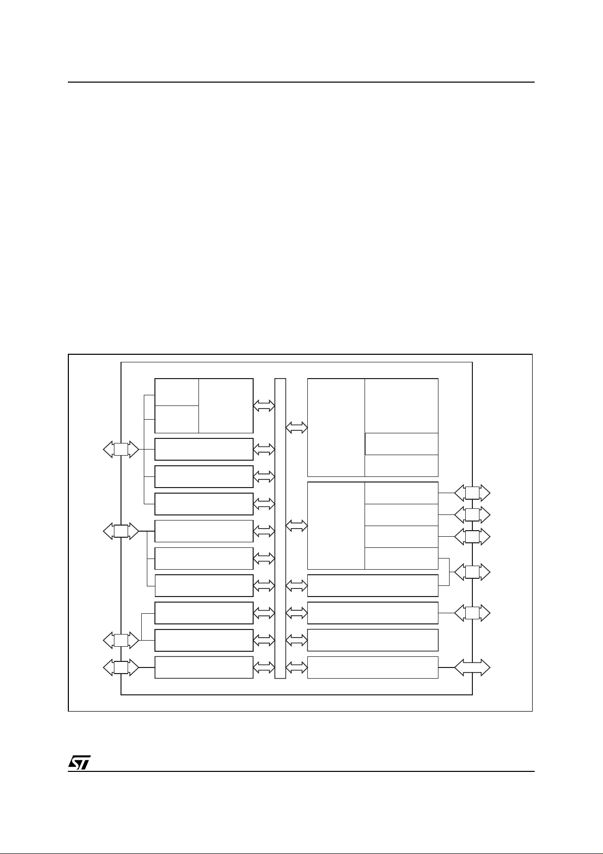
The uPSD323x Series combines a fast 8051based microcontroller with a flexible memory
structure, programmable logic, and a rich peripheral mix including USB, to form an ideal embedded
controller. At its core is an industry-standard 8032
MCU operating up to 40MHz.
A JTAG serial interface is used for In-System Programming (ISP) in as little as 10 seconds, perfect
for manufacturing and lab development.
The USB 1.1 low-speed interface has one Control
endpoint and two I nterrupt endpoints suitable f or
HID class drivers.
The 8032 core is coupled to Programmable System Device (PSD) architecture to optimize the
8032 memory structure, offering two independent
banks of Flash mem ory that can be pl aced at virtually any address within 8032 program or data address space, and easily paged beyond 64K bytes
using on-chip programmable decode logic.
Figure 2. Block Diagram
Dual Flash memory banks provide a robust solution for remote product updates in the field through
In-Application Programming (IAP). Dual Flash
banks also support EEPROM emulation, eliminating the need for exte r n al EEPROM chips.
General purpose programmable logic (PLD) is included to build an endless variety of glue-logic,
saving external logic devices. The PLD is conf igured using the software development tool, PSDsoft Express, available from the web at
www.st.com/psm, at no charge.
The uPSD323x also includes supervisor functions
such as a programmable watchdog timer and lowvoltage reset.
P3.0:7
P1.0:7
P4.0:7
USB+,
USB–
(3) 16-bit
Timer/
Counters
(2)
External
Interrupts
(8) GPIO, Port 3
(8) GPIO, Port 1
(4) 8-bit ADC
(5) 8-bit PWM
(8) GPIO, Port 4
I2C
UART0
UART1
USB v1.1
8032
MCU
Core
uPSD323x
Programmable
Programmable
SYSTEM BUS
1st Flash Memory:
128K or 256K Bytes
Decode and
Page Logic
General
Purpose
Logic,
16 Macrocells
8032 Address/Data/Control Bus
Watchdog and Low-Voltage Reset
VCC, VDD, GND, Reset, Crystal In
2nd Flash Memory:
32K Bytes
SRAM:
8K Bytes
(8) GPIO, Port A
(80-pin only)
(8) GPIO, Port B
(2) GPIO, Port D
(4) GPIO, Port C
JTAG ISP
(80-pin device only)
Supervisor:
PA0:7
PB0:7
PD1:2
PC0:7
MCU
Bus
Dedicated
Pins
AI10429
7/170
uPSD3234A, uPSD3234BV, uPSD3233B, uPSD3233BV
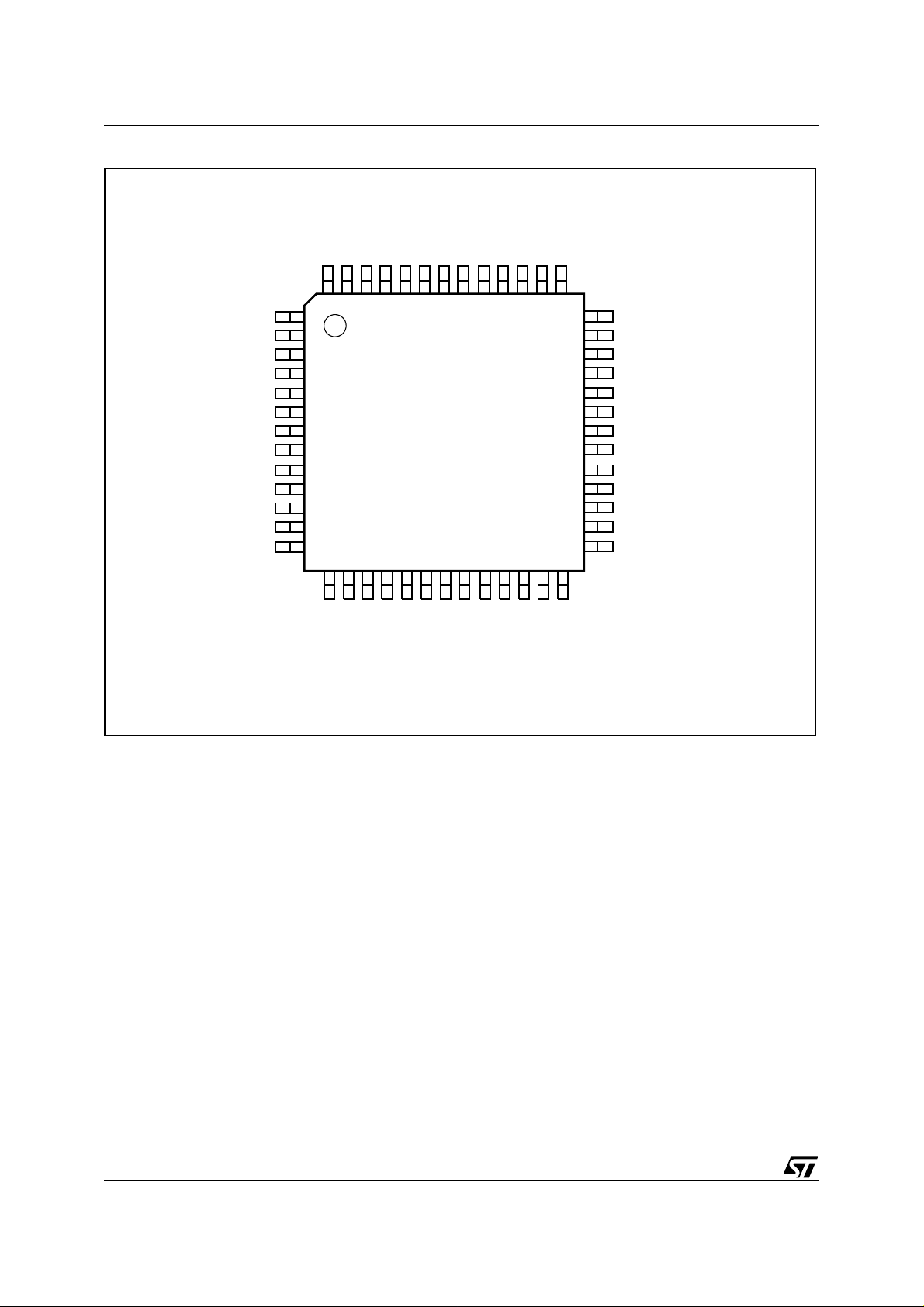
Figure 3. TQ FP 52 Connection s
PB0
PB1
PB2
PB3
PB4
PB5
VREF
GND
RESET_
PB6
PB7
52515049484746454443424140
P1.7/ADC3
P1.6/ADC2
PC7
(1)
USB+
V
CC
GND
STBY
1
2
3
4
5
6
7
8
9
10
11
12
13
14151617181920212223242526
P4.7/PWM4
P4.6/PWM3
P4.5/PWM2
P4.4/PWM1
GND
SYNC
P4.3/PWM0
P4.2/DDC V
P3.1/TXD
P3.0/RXD
P4.1/DDC SCL
P4.0/DDC SDA
P3.2/EXINT0
P3.3/EXINT1
39 P1.5/ADC1
38 P1.4/ADC0
37 P1.3/TXD1
36 P1.2/RXD1
35 P1.1/T2X
34 P1.0/T2
33 V
CC
32 XTAL2
31 XTAL1
30 P3.7/SCL1
29 P3.6/SDA1
28 P3.5/T1
27 P3.4/T0
AI07423b
PD1/CLKIN
JTAG TDO
JTAG TDI
USB–
PC4/TERR_
PC3/TSTAT
PC2/V
JTAG TCK
JTAG TMS
Note: 1. Pull-up re si stor re quired on pin 5 (2 k Ω for 3V devices, 7.5k Ω for 5V devices) for all 52-pi n devices, wi th or without USB function.
8/170
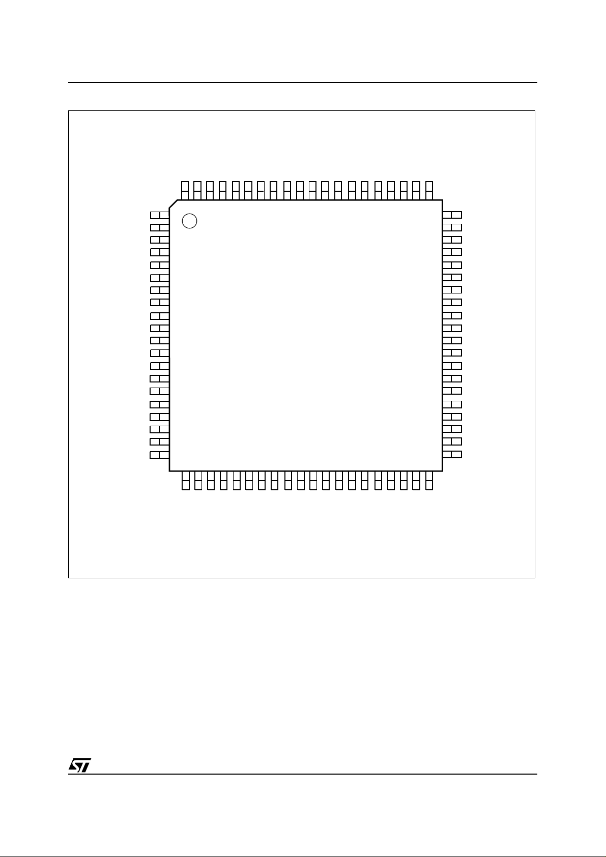
Figure 4. TQ FP 80 Connection s
PB0
P3.2/EXINT0
80797877767574737271706968676665646362
PD2
1
P3.3 /EXINT1
PD1/CLKIN
JTAG/TDO
JTAG/TDI
USB–
PC4/TERR_
PC3/TSTAT
PC2/V
JTAG TCK
P4.7/PWM4
P4.6/PWM3
JTAG TMS
ALE
PC7
(1)
USB+
(2)
NC
V
CC
GND
STBY
(2)
NC
2
3
4
5
6
7
8
9
10
11
12
13
14
15
16
17
18
19
20
PB1
P3.1/TXD0
uPSD3234A, uPSD3234BV, uPSD3233B, uPSD3233BV
(2)
PB2
P3.0/RXD0
PB3
PB4
PB5
NC
REF
V
GND
RESET_
PB6
PB7
RD_
P1.7/ADC3
PSEN_
WR_
P1.6/ADC2
61
60 P1.5/ADC1
59 P1.4/ADC0
58 P1.3/TXD1
57 A11
56 P1.2/RXD1
55 A10
54 P1.1/TX2
53 A9
52 P1.0/T2
51 A8
50 V
CC
49 XTAL2
48 XTAL1
47 AD7
46 P3.7/SCL1
45 AD6
44 P3.6/SDA1
43 AD5
42 P3.5/T1
41 AD4
21222324252627282930313233343536373839
PA7
PA6
PA5
PA4
P4.5/PWM2
P4.4/PWM1
P4.3/PWM0
Note: 1. Pull-up re si stor re quired on pin 8 (2 k Ω for 3V devices, 7.5k Ω for 5V devices) for all 82-pi n devices, wi th or without USB function.
2. NC = Not Connected
PA3
GND
SYNC
P4.2/DDC V
PA2
PA1
P4.1/DDC SCL
P4.0/DDC SDA
PA0
AD0
AD1
AD2
40
AD3
P3.4/T0
AI07424b
9/170

uPSD3234A, uPSD3234BV, uPSD3233B, uPSD3233BV
Table 2. 80-Pin Package Pin Description
Port Pin
Signal
Name
Pin No. In/Out
AD0 36 I/O
Basic Alternate
External Bus
Multiplexed Address/Data bus A1/D1
AD1 37 I/O Multiplexed Address/Data bus A0/D0
AD2 38 I/O Multiplexed Address/Data bus A2/D2
AD3 39 I/O Multiplexed Address/Data bus A3/D3
AD4 41 I/O Multiplexed Address/Data bus A4/D4
AD5 43 I/O Multiplexed Address/Data bus A5/D5
AD6 45 I/O Multiplexed Address/Data bus A6/D6
AD7 47 I/O Multiplexed Address/Data bus A7/D7
P1.0 T2 52 I/O General I/O port pin Timer 2 Count input
P1.1 TX2 54 I/O General I/O port pin Timer 2 Trigger input
P1.2 RxD1 56 I/O General I/O port pin 2nd UART Receive
P1.3 TxD1 58 I/O General I/O port pin 2nd UART Transmit
P1.4 ADC0 59 I/O General I/O port pin ADC Channel 0 input
P1.5 ADC1 60 I/O General I/O port pin ADC Channel 1 input
P1.6 ADC2 61 I/O General I/O port pin ADC Channel 2 input
P1.7 ADC3 64 I/O General I/O port pin ADC Channel 3 input
Function
A8 51 O External Bus, Address A8
A9 53 O External Bus, Address A9
A10 55 O External Bus, Address A10
A11 57 O External Bus, Address A11
P3.0 RxD0 75 I/O General I/O port pin UART Receive
P3.1 TxD0 77 I/O General I/O port pin UART Transmit
P3.2 EXINT0 79 I/O General I/O port pin
P3.3 EXINT1 2 I/O General I/O port pin
Interrupt 0 input / Timer 0 gate
control
Interrupt 1 input / Timer 1 gate
control
P3.4 T0 40 I/O General I/O port pin Counter 0 input
P3.5 T1 42 I/O General I/O port pin Counter 1 input
P3.6 SDA1 44 I/O General I/O port pin
P3.7 SCL1 46 I/O General I/O port pin
2
I
C Bus serial data I/O
2
I
C Bus clock I/O
P4.0 DDC SDA 33 I/O General I/O port pin
P4.1 DDC SCL 31 I/O General I/O port pin
P4.2
P4.3 PWM0 27 I/O General I/O port pin
DDC V
SYNC
30 I/O General I/O port pin
8-bit Pulse Width Modulation
output 0
10/170
uPSD3234A, uPSD3234BV, uPSD3233B, uPSD3233BV
Port Pin
P4.4 PWM1 25 I/O General I/O port pin
P4.5 PWM2 23 I/O General I/O port pin
P4.6 PWM3 19 I/O General I/O port pin
P4.7 PWM4 18 I/O General I/O port pin
Signal
Name
USB– 8 I/O
V
REF
RD_ 65 O READ signal, external bus
WR_ 62 O WRITE signal, external bus
PSEN_ 63 O PSEN
ALE 4 O Address Latch signal, external bus
RESET_ 68 I Active low RESET
XTAL1 48 I Oscillator input pin for system clock
XTAL2 49 O Oscillator output pin for system clock
Pin No. In/Out
Pull-up resistor required (2kΩ for 3V
devices, 7.5kΩ for 5V devices)
70 O Reference Voltage input for ADC
signal, external bus
Function
Basic Alternate
8-bit Pulse Width Modulation
output 1
8-bit Pulse Width Modulation
output 2
8-bit Pulse Width Modulation
output 3
Programmable 8-bit Pulse Width
modulation output 4
input
PA0 35 I/O General I/O port pin
PA1 34 I/O General I/O port pin
PA2 32 I/O General I/O port pin
PA3 28 I/O General I/O port pin
PA4 26 I/O General I/O port pin
PA5 24 I/O General I/O port pin
PA6 22 I/O General I/O port pin
PA7 21 I/O General I/O port pin
PB0 80 I/O General I/O port pin
PB1 78 I/O General I/O port pin
PB2 76 I/O General I/O port pin
PB3 74 I/O General I/O port pin
PB4 73 I/O General I/O port pin
PB5 72 I/O General I/O port pin
PB6 67 I/O General I/O port pin
PB7 66 I/O General I/O port pin
1. PLD Macro-cell outputs
2. PLD inputs
3. Latched Address Out (A0A7)
4. Peripheral I/O Mode
1. PLD Macro-cell outputs
2. PLD inputs
3. Latched Address Out (A0A7)
11/170

uPSD3234A, uPSD3234BV, uPSD3233B, uPSD3233BV
Port Pin
PC2
PC3 TSTAT 14 I/O General I/O port pin
PC4 TERR_ 9 I/O General I/O port pin
PC7 5 I/O General I/O port pin
PD1 CLKIN 3 I/O General I/O port pin
PD2 1 I/O General I/O port pin
Vcc 12
Vcc 50
GND 13
GND 29
GND 69
Signal
Name
JTAG TMS 20 I JTAG pin
JTAG TCK 16 I JTAG pin
V
STBY
JTAG TDI 7 I JTAG pin
JTAG TDO 6 O JTAG pin
USB+ 10
Pin No. In/Out
15 I/O General I/O port pin
Function
Basic Alternate
1. PLD Macro-cell outputs
2. PLD inputs
3. SRAM stand by voltage input (V
4. SRAM battery-on indicator
(PC4)
5. JTAG pins are dedicated
pins
1. PLD I/O
2. Clock input to PLD and APD
1. PLD I/O
2. Chip select to PSD Module
STBY
)
NC 11
NC 17
NC 71
52-PIN PACKAGE I/O PORT
The 52-pin package members of the uPSD323X
Devices have the sam e port pins as those of t he
80-pin package except:
■ Port 0 (P0.0-P0.7, external address/data bus
AD0-AD7)
■ Port 2 (P2.0-P2.3, external address bus A8-
A11)
■ Port A (PA0-PA7)
■ Port D (PD2)
■ Bus control signal (RD,WR,PSEN,ALE)
Pin 5 requires a pull-up resistor (2kΩ for 3V
devices, 7.5k Ω for 5V devices) for all devices,
with or without USB function.
12/170

uPSD3234A, uPSD3234BV, uPSD3233B, uPSD3233BV
ARCHITECTURE OVERVIEW
Memory Organization
The uPSD323X Devices’s standard 8032 Core
has separate 64KB address spac es for Program
memory and Data Memory. Program memory is
where the 8032 executes in structions from. Data
memory is used to hold data variables. Flash
memory can be mapped in either program or data
space. The Flash memory consists of two flash
memory blocks: the main Flash (1 or 2Mbit) and
the Secondary Flash (256Kbit). Except during
flash memory programming or update, Flash
memory can only be read, not written to. A Page
Register is used to access memory beyond the
64K bytes address space. Refer to the PSD Module for details on mapping of the Flash memory.
Figure 5. Memory Map and Address Space
MAIN
FLASH
The 8032 core h as t wo t ypes of data memory (internal and external) that can be read and written.
The internal SRAM consists o f 256 byte s, and includes the stack area.
The SFR (Special Function Registers) occupies
the upper 128 bytes of the internal SRAM, the registers can be accessed by Direct addressing only.
There are two separate blocks of external SRAM
inside the uPSD323X Devices: one 256 bytes
block is assigned for DDC data storage. Anot her
8K bytes resides in the PSD Modu le that can be
mapped to any address space defined by the user.
EXT. RAM
INT. RAM
SECONDARY
FLASH
32KB
Flash Memory Space
128KB
OR
256KB
FF
Indirect
Addressing
7F
Indirect
Direct
Addressing
0
Internal RAM Space
(256 Bytes)
or
Registers
The 8032 has several registers; these are the Program Counter (PC), Accumulator (A), B Register
(B), the Stack Pointer (SP), the Program Status
Word (PSW), General purpose registers (R0 to
R7), and DPTR (Data Pointer register).
EXT. RAM
FFFF
FF00
(DDC)
External RAM Space
(MOVX)
SFR
Direct
Addressing
Figure 6. 8032 MCU Registers
A
B
SP
PCH
DPTR(DPH)
PCL
PSW
R0-R7
DPTR(DPL)
8KB256B
AI06635
Accumulator
B Register
Stack Pointer
Program Counter
Program Status Word
General Purpose
Register (Bank0-3)
Data Pointer Register
AI06636
13/170
uPSD3234A, uPSD3234BV, uPSD3233B, uPSD3233BV
Accumulator. The Accumulator is the 8-bit gen-
eral purpose register, used for data operation such
as transfer, temporary saving, and conditional
tests. The Accumulator can be used as a 16-bit
register with B Register as shown below.
Figure 7. Configuration of BA 16-bit Registers
B
AB
A
Two 8-bit Registers can be used as a "BA" 16-bit Registers
AI06637
B Register. The B Register is the 8-bit general
purpose register, used for an arithmetic operation
such as multiply, division with Accumulator
Stack Pointer. The Stack Pointer Register is 8
bits wide. It is incremented before data is stored
during PUSH and CALL executions. While the
stack may reside anywhere in on-chip RAM, the
Stack Po inter is in itializ ed to 07 h a fter res et. T his
causes the stack to begin at location 08h.
Figure 8. Stack Pointer
Stack Area (30h-FFh)
Bit 15 Bit 0Bit 8 Bit 7
Hardware Fixed
SP (Stack Pointer) could be in 00h-FFh
SP00h
00h-FFh
AI06638
Program Counter. The Program Counter is a 16bit wide which consists of two 8-bit registers, PCH
and PCL. This counter indicates the address of the
next instruction to be executed. In RESET
state,
the program counter has reset routine address
(PCH:00h, PCL:00h).
Program Status Word. The Program Status
Word (PSW) contains several bits that reflect the
current state of the CPU and select Internal RAM
(00h to 1Fh: Bank0 to Bank3). The PSW is described in Figure 9., page 15. It contains the Carry
flag, the Auxiliary carry flag, the Half Carry (for
BCD operation), the general purpose flag, the
Register bank select flags, the Overflow flag, and
Parity flag .
[Carry Flag, CY]. This flag stores any carry or not
borrow from the ALU of CPU after an arithmetic
operation and is also changed by the Shift Instruction or Rotate Instruction.
[Auxiliary Carry Flag, AC]. After operation, this is
set when there is a carry from Bit 3 of ALU or there
is no borrow from Bit 4 of ALU.
[Register Bank Select Flags, RS0, RS1]. This flags
select one of four bank(00~07H:bank0,
08~0Fh:bank1, 10~17h: bank2, 17~1Fh:bank3) in
Internal RAM.
[Overflow Flag, OV]. This flag is set to '1' when an
overflow occurs as the result of an arithmetic operation involving signs. An overflow occurs when the
result of an addition or subtraction exceeds +127
(7Fh) or -128 (80h). The CLRV instruction clears
the overflow flag. There is no set instruction. When
the BIT instruction is executed, Bit 6 of memory is
copied to this flag.
[Parity Flag, P]. This flag reflect on number of Accumulator’s 1. If number of Accumulator’s 1 is odd,
P=0. otherwise P=1. Sum of adding Accumulator’s
1 to P is always even.
R0~R7. General purpose 8-bit registers that are
locked in the lower portion of internal data area.
Data Pointer Register. Data Pointer Register is
16-bit wide which consists of two-8bit registers,
DPH and DPL. This register is used as a data
pointer for the data transmission with external data
memory in the PSD Module.
14/170

uPSD3234A, uPSD3234BV, uPSD3233B, uPSD3233BV
Figure 9. PSW (Program Stat us W o rd) Re gi st er
MSB
CY
PSW
Carry Flag
Auxillary Carry Flag
General Purpose Flag
AC FO RS1RS0 OV P
Register Bank Select Flags
(to select Bank0-3)
Program Memory
The program memory consists of two Flash memory: 128 KByte (or 256 KByte) Main Flash and 32
KByte of Secondary Flash. The Flash memory can
be mapped to any address space as defined by
the user in the PSDsoft Tool. It can also be
mapped to Data memory space during Flash
memory update or programming.
After reset, the CPU begins execution from location 0000h. As shown in Figure 10, e ach interrupt
is assigned a fixed location in Program Memory.
The interrupt causes the CPU to jump to that location, where it commences execution of the service
routine. External Interrupt 0, for example, is assigned to location 0003h. If External Interrupt 0 is
going to be used, its service routine must begin at
location 0003h. If the interrupt is not going to be
used, its service location is available as gen eral
purpose Pro-gram Memory.
The interrupt service locations are spaced at 8byte intervals: 0003h for External Interrupt 0,
000Bh for Timer 0, 0013 h for E xternal I nterrupt 1,
001Bh for Timer 1 and so forth. If an interrupt service routine is short enough (as is often the cas e
in control applications), it can reside entirely within
that 8-byte interval. Longer service routines can
use a jump instruction to skip over subsequent interrupt locations, if other interrupts are in use.
Data memory
The internal data memory is divided into four physically separ ated blocks: 256 byt es of internal RAM,
128 bytes of Special Function Registers (SFRs)
areas, 256 bytes of external RAM (XRAM-DDC)
and 8K bytes (XRAM-PSD) in the PSD Module.
RAM
Four register banks, each 8 registers wide, occupy
locations 0 through 31 in the lower RAM area.
Only one of these banks may be enabled at a time.
The next 16 bytes, locations 32 through 47, contain 128 directly addressable bit locations. The
stack depth is only limited by the available internal
RAM space of 256 bytes.
LSB
Reset Value 00h
Parity Flag
Bit not assigned
Overflow Flag
AI06639
Figure 10. Int errupt Locatio n of Program Memory
008Bh
•
•
•
•
0013h
000Bh
0003h
0000hReset
8 Bytes
AI06640
Interrupt
Location
•
•
•
•
•
XRAM-DDC
The 256 bytes of XRAM-DDC used to support
DDC interface is also available for system usage
by indirect addressing through the address pointer
DDCADR and data I/O buffer RAMBUF. The address pointer (DDCADR) is equipped with the post
increment capability to facilitate the transfer of
data in bulk (for details refer to DDC Interface
part). However, it is also possible to address t he
RAM through MOVX comm and as normally used
in the internal RAM extension of 80C51 derivatives. XRAM-DDC FF00 to FFFF is directly addressable as external data memory locations
FF00 to FFFF via MOVX-DPTR inst ruction or via
MOVX-Ri instruction. When XRAM-DDC is disabled, the address space FF00 to FFFF can be assigned to other resources.
XRAM-PSD
The 8K bytes of XRAM-PS D resides in the PSD
Module and can be mapped to any address space
through the DPLD (Decoding PLD) as defined by
the user in PSDsoft Development tool. The XRAMPSD has a battery backup feature that allow the
data to be retained in t he event of a power lost.
The battery is connected t o the Port C PC2 pin.
This pin must be configured in PSDSoft to be battery back-up.
15/170

uPSD3234A, uPSD3234BV, uPSD3233B, uPSD3233BV
SFR
The SFRs can only be addressed directly in the
address range from 80h to FFh. Table
15., page 28 gives an overview of the Special
Function Registers. Sixteen address in the SFRs
space are both-byte and bit-addressable. Th e bi taddressable SFRs are those whose address ends
in 0h and 8h. The bit addresses in this area are
80h to FFh.
Addressing Modes
The addressing modes in uPSD323X Devices instruction set are as follows
■ Direct addressing
■ Indirect addressing
■ Register addressing
■ Register-specific addressing
■ Immediate constants addressing
■ Indexed addressing
Table 3. RAM Address
Byte Address
(in Hexadecimal)
↓↓
FFh 255
30h 48
msb Bit Address (Hex) lsb
Byte Address
(in Decimal)
(1) Direct addressing. In a direct addressing the
operand is specified by an 8-bit address field in the
instruction. Only internal Data RAM and SFRs
(80~FFH RAM) can be directly addressed.
Example:
mov A, 3EH ; A <----- RAM[3E]
Figure 11. Direct Addressing
2Fh 7F 7E 7D 7C 7B 7A 79 78 47
2Eh777675747372717046
2Dh 6F 6E 6D 6C 6B 6A 69 68 45
2Ch676665646362616044
Program Memory
3Eh
04
A
2Bh 5F 5E 5D 5C 5B 5A 59 58 43
2Ah575655545352515042
29h 4F 4E 4D 4C 4B 4A 49 48 41
28h 47 46 45 44 43 42 41 40 40
27h 3F 3E 3D 3C 3B 3A 39 38 39
26h 37 36 35 34 33 32 31 30 38
25h 2F 2E 2D 2C 2B 2A 29 28 37
24h 27 26 25 24 23 22 21 20 36
23h 1F 1E 1D 1C 1B 1A 19 18 35
22h 17 16 15 14 13 12 11 10 34
21h 0F 0E 0D 0C 0B 0A 09 08 33
20h 07 06 05 04 03 02 01 00 32
1Fh
Register Bank 3
18h 24
17h
Register Bank 2
10h 16
0Fh
Register Bank 1
08h 8
07h
Register Bank 0
00h 0
31
23
15
7
AI06641
(2) Indirect addressing. In indirect addressing
the instruction specifies a register which cont ains
the address of the operand. Both internal and external RAM can be indirectly addressed. The address register for 8-bit addresses can be R0 or R1
of the selected register bank, or the Stack Pointer.
The address register for 16-bit addresses can only
be the 16-bit “data pointer” register, DPTR.
Example:
mov @R1, #40 H ;[R1] <-----40H
Figure 12. Indi rect Address in g
Program Memory
55h
R1
40h
55
AI06642
16/170
uPSD3234A, uPSD3234BV, uPSD3233B, uPSD3233BV
(3) Register addressing. The register banks,
containing registers R0 through R7, can be accessed by certain instruction s which carry a 3-bit
register specification within the o pcode of the instruction. Instructions that access the registers
this way are code efficient, since this m ode eliminates an address byte. When the instruction is executed, one of four banks is selected at execution
time by the two bank select bits in the PSW.
Example:
mov PSW, #0001000B ; select Bank0
mov A, #30H
mov R1, A
(4) Register-specific addressing. Some instructions are specific to a certain register. For example, some instructions always operate on the
Accumulator, or Data Pointer, etc., so no addres s
byte is needed to point it. The opcode it self does
that.
(5) Immediate constants addressing. The value of a constant can follow the opcode in Program
memory.
Example:
mov A, #10H.
(6) Indexed addressing. Only Program me mory
can be accessed with indexed addressing, a nd it
can only be read. This addressing mode is intended for reading look-up tables in Program memory.
A 16-bit base register (either DPTR or PC) points
to the base of the table, and the Accumulator is set
up with the table entry number. The address of the
table entry in Program memory is formed by adding the Accumulator data to the base pointer.
Example:
movc A, @A+DPTR
Figure 13. Indexed Addre ssing
ACC DPTR
3Ah 1E73h
Program Memory
Arithmetic Instructions
The arithmetic instructions is listed in Table
4., page 18. The table indicates the addressing
modes that can be used with each i nstruction to
access the <byte> operand. For example, the
ADD A, <byte> instruction can be written as:
ADD a, 7FH (direct addressing)
ADD A, @R0 (indirect addressing)
ADD a, R7 (register addressing)
ADD A, #127 (immediate constant)
Note: Any byte in the internal Data Memory space
can be incremented without going through the Accumulator.
One of the INC instructions operates on the 16-bit
Data Pointer. The Data Pointer is used to generate
16-bit addresses for external memory, so being
able to increment it in one 16-bit operations is
a useful feature.
The MUL A B instruc tion mul tiplies the Accum ula-
tor by the data in the B register and puts the 16-bit
product into the concatenated B and Acc um ulator
registers.
The DIV AB instruction divides the Accumulator by
the data in the B register and leaves the 8-bit quotient in the Accumulator, and the 8-bit remainder in
the B regi ste r.
In shift operations, dividing a num ber by 2n s hifts
its “n” bits to the right. Using DIV AB t o perform the
division completes the shift in 4?s and leaves the
B register holding the b its that were shifted out.
The DAA instruction is for BCD arithmetic operations. In BCD arithmetic, ADD and ADDC instructions should always be followed by a DAA
operation, to ensure that the result is also in BCD.
Note: DAA will not convert a binary number to
BCD. The DAA operation produces a meaningful
result only as the second step in the addition of
two BCD bytes.
AI06643
3Eh
17/170

uPSD3234A, uPSD3234BV, uPSD3233B, uPSD3233BV
Table 4 . Arithm etic Instructio n s
Mnemonic Operation
ADD A,<byte> A = A + <byte> X X X X
ADDC A,<byte> A = A + <byte> + C X X X X
SUBB A,<byte> A = A – <byte> – C X X X X
INC A = A + 1 Accumulator only
INC <byte> <byte> = <byte> + 1 X X X
INC DPTR DPTR = DPTR + 1 Data Pointer only
DEC A = A – 1 Accumulator only
DEC <byte> <byte> = <byte> – 1 X X X
MUL AB B:A = B x A Accumulator and B only
DIV AB
DA A Decimal Adjust Accumulator only
A = Int[ A / B ]
B = Mod[ A / B ]
Dir. Ind. Reg. Imm
Logical Instructions
Table 5., page 19 shows list of uPSD323X Devic-
es logical instructions. The instructions that perform Boolean operations (AND, OR, Exclusive
OR, NOT) on bytes perform the operation on a bitby-bit basis. That is, if th e Accumulator contains
00110101B and byte contains 01010011B, then:
ANL A, <byte>
will leave the Accum u lator holdi ng 00010001B.
The addressing modes that can be used to access
the <byte> operand are listed in Table 5., page 19.
The ANL A, <byte> instruction may take any of the
forms:
ANL A,7FH(direct addressing)
ANL A, @R1 (indirect addressing)
ANL A,R6 (register addressing)
ANL A,#53H (immediate constant)
Note: Boolean operations can be performed on
any byte in the internal Data Mem ory space without going through the Accumulator. The XRL
<byte>, #data instruction, for example, offers a
quick and easy way to invert port bits, as in
If the operation is in response to an interrupt, not
using the Accumulator saves the time and effort to
push it onto the stack in the service routine.
The Rotate instructions (RL A , RLC A, etc.) shift
the Accumulator 1 bit to the left or right. For a left
rotation, the MSB rolls into the LSB position. For a
right rotation, the LSB rolls into the MSB position.
The SWAP A instruction interchanges the high
and low nibbles within the Accumulator. This is a
useful operation in BCD manipulations. For example, if the Accumulator contains a binary num ber
which is known to be less than 100, it can be quickly converted to BCD by the following code:
MOVE B,#10
DIV AB
SWAP A
ADD A,B
Dividing the number by 10 leaves the tens digit in
the low nibble of the Acc umulator, and the ones
digit in the B register. The SWAP and ADD instructions move the tens digit to the high nibble of the
Accumulator, and the ones digit to the low nibble.
XRL P1, #0FFH.
Addressing Modes
Accumulator and B only
18/170
uPSD3234A, uPSD3234BV, uPSD3233B, uPSD3233BV
Table 5. Logical Instructions
Mnemonic Operation
Dir. Ind. Reg. Imm
ANL A,<byte> A = A .AND. <byte> X X X X
ANL <byte>,A A = <byte> .AND. A X
ANL <byte>,#data A = <byte> .AND. #data X
ORL A,<byte> A = A .OR. <byte> X X X X
ORL <byte>,A A = <byte> .OR. A X
ORL <byte>,#data A = <byte> .OR. #data X
XRL A,<byte> A = A .XOR. <byte> X X X X
XRL <byte>,A A = <byte> .XOR. A X
XRL <byte>,#data A = <byte> .XOR. #data X
CRL A A = 00h Accumulator only
CPL A A = .NOT. A Accumulator only
RL A Rotate A Left 1 bit Accumulator only
RLC A Rotate A Left through Carry Accumulator only
RR A Rotate A Right 1 bit Accumulator only
Addressing Modes
RRC A Rotate A Right through Carry Accumulator only
SWAP A Swap Nibbles in A Accumulator only
19/170
uPSD3234A, uPSD3234BV, uPSD3233B, uPSD3233BV
Data Transfers
Internal RAM. Table 6 shows the menu of in-
structions that are available for moving data
around within the internal memory spaces, and the
addressing modes that can be used with each
one. The MOV <dest>, <src> instruction allows
data to be transferred between any two internal
RAM or SFR locations without going through the
Accumulator. Remember, the Uppe r 128 b ytes of
data RAM can be accessed only by indirect addressing, and SFR space only by di rect addressing.
Note: In uPSD323X Devices, the stack resides in
on-chip RAM, and grows upwards. T he PUSH instruction first increments the Stac k Pointer (SP),
then copies the byte into the stack. PUSH and
POP use only direct addressing to identify the byte
being saved or restored, but the stack itself is accessed by indirect addressing using the S P register. This means the stack can go into the Upper
128 bytes of RAM, if they are implemented, but not
into SFR space.
The Data Transfer instructions include a 16-bit
MOV that can be used to initialize the Data Pointer
(DPTR) for look-up tables in Program Memory.
The XCH A, <byte> instruction causes the Accumulator and ad-dressed byte to exchange data.
The XCHD A, @Ri instruction is similar, but only
the low nibbles are involved in the exchange. To
see how XCH and XCHD can be used to facilitate
data manipulations, consider first the problem of
shifting and 8-digit BCD number two digits to the
right. Table 8., page 21 shows how this can be
done using XCH instructions. To aid in understanding how the code works, the contents of the
registers that are holding the BCD number and the
content of the Accumulator are shown alon gside
each instruction to indicate their status after the instruction has been executed.
After the routine has been executed, the Accumulator contains the two digits that were shifted out
on the right. Doing the routine with direct MOVs
uses 14 code bytes. The same operation with
XCHs uses only 9 bytes and executes almost
twice as fast. To right-shift by an odd number of
digits, a one-digit must be executed. Table
9., page 21 shows a sample of code that will right-
shift a BCD number one digit, using the XCHD instruction. Again, the contents of the registers holding the number and of the accumulator are shown
alongside each instruction.
Table 6. Data Transfer Instructions that Access Internal Data Memory Space
Mnemonic Operation
Dir. Ind. Reg. Imm
MOV A,<src> A = <src> XXXX
MOV <dest>,A <dest> = A X X X
MOV <dest>,<src> <dest> = <src> XXXX
MOV DPTR,#data16 DPTR = 16-bit immediate constant X
PUSH <src> INC SP; MOV “@SP”,<src> X
POP <dest> MOV <dest>,”@SP”; DEC SP X
XCH A,<byte> Exchange contents of A and <byte> X X X
XCHD A,@Ri Exchange low nibbles of A and @Ri X
Addressing Modes
20/170
uPSD3234A, uPSD3234BV, uPSD3233B, uPSD3233BV
First, pointers R1 and R0 are set up to point to the
two bytes containing the last four BCD digits. Then
Table 7. Shifting a BCD Number Two Digits to the Right (using direct MOVs: 14 bytes)
a loop is executed which leaves the last byte, location 2EH, holding the l ast two dig its of the s hifted
number. The pointers are decremented, and the
loop is repeated for location 2DH. The CJNE instruction (Compare and Jump if Not equal) is a
loop control that will be des cribed later. The loop
MOV A,2Eh 00 12 34 56 78 78
MOV 2Eh,2Dh 00 12 34 56 56 78
MOV 2Dh,2Ch 00 12 34 34 56 78
executed from LOOP to CJNE for R1 = 2EH, 2DH,
2CH, and 2BH. At that point the digit that was originally shifted out on the right has propagated to location 2AH. Since that location should be left with
MOV 2Ch,2Bh 00 12 12 34 56 78
MOV2Bh,#0 0000123456 78
0s, the lost digit is moved to the Accumulator.
Table 8. Shifting a BCD Number Two Digits to the Right (using direct XCHs: 9 bytes)
CLR A 00 12 34 56 78 00
XCH A,2Bh 00 00 34 56 78 12
XCH A,2Ch 00 00 12 56 78 34
XCH A,2Dh 00 00 12 34 78 56
XCH A,2Eh 00 00 12 34 56 78
Table 9. Shifting a BCD Number One Digit to the Right
2A 2B 2C 2D 2E ACC
MOV R1,#2Eh 00 12 34 56 78 xx
MOV R0,#2Dh 00 12 34 56 78 xx
2A 2B 2C 2D 2E ACC
2A 2B 2C 2D 2E ACC
; loop for R1 = 2Eh
LOOP:MOV A,@R1 0012345678 78
XCHD A,@R0 0012345878 76
SWAP A 00 12 34 58 78 67
MOV @R1,A 00 12 34 58 67 67
DEC R1 0012345867 67
DEC R0 0012345867 67
CNJE R1,#2Ah,LOOP 00 12 34 58 67 67
; loop for R1 = 2Dh 00 12 38 45 67 45
; loop for R1 = 2Ch 00 18 23 45 67 23
; loop for R1 = 2Bh 08 01 23 45 67 01
CLR A 08 01 23 45 67 00
XCH A,2Ah 00 01 23 45 67 08
21/170
uPSD3234A, uPSD3234BV, uPSD3233B, uPSD3233BV
External RAM. Table 10 shows a l ist of the Data
Transfer instructions that access external Data
Memory. Only indirect addressing can be used.
The choice is whether to us e a one-by te address,
@Ri, where Ri can be either R0 or R1 of the s elected register bank, or a two-byte
address, @DTPR.
Note: In all external Data RAM accesses, the Accumulator is always either the destination or
source of the data.
Lookup Tables. Table 11 shows the two instruc-
tions that are available for reading lookup tables in
Program Memory. Since these instructions access
only Program Memory, the lookup tables can only
be read, not updated.
The mnemonic is MOVC for “move constant.” The
first MOVC instruction in Table 11 can accommo-
date a table of up to 256 entries numbered 0
through 255. The number of th e desired entry is
loaded into the Accumulator, and the Data Pointer
is set up to point to the beginning of the table.
Then:
MOVC A, @A+DPTR
copies the desired table entry into the Accumula-
tor.
The other MOVC instruction works the same way,
except the Program Counter (PC) is used as the
table base, and the table is accessed th rough a
subroutine. First the number of the desired en-try
is loaded into the Accumulator, and the subroutine
is called:
MOV A , ENTRY NUMBER
CAL L TAB LE
The subroutine “TABLE” would look like this:
TABLE: MO VC A , @ A+PC
RET
The table itself immediately follows the RET (return) instruction is Program Memory. This type of
table can have up to 255 entries, numbered 1
through 255. Number 0 cannot b e used, because
at the time the MOVC instruction is executed, the
PC contains the address of the RET instru ction.
An entry numbered 0 would be the RET opcode itself.
Table 10. Data Transfer Instruction that Access External Data Memory Space
Address Width Mnemonic Operation
8 bits MOVX A,@Ri READ external RAM @Ri
8 bits MOVX @Ri,A WRITE external RAM @Ri
16 bits MOVX A,@DPTR READ external RAM @DPTR
16 bits MOVX @DPTR,a WRITE external RAM @DPTR
Table 11. Lookup Table READ Instruction
Mnemonic Operation
MOVC A,@A+DPTR READ program memory at (A+DPTR)
MOVC A,@A+PC READ program memory at (A+PC)
22/170

uPSD3234A, uPSD3234BV, uPSD3233B, uPSD3233BV
Boolean Instructions
The uPSD323X Devices contain a complete Boolean (single-bit) processor. One page o f the internal RAM contains 128 address -able bits, and the
SFR space can support up to 128 addressable bits
as well. All of the port lines are bit-addressable,
and each one can be treated as a separate singlebit port. The instructions that access these bits are
not just conditional branches, but a complete
menu of move, set, clear, complement, OR and
AND instructions. These kinds of bit operations
are not easily obtained in other architectures with
any amount of byte-oriented software.
The instruction set for the Boolean processor is
shown in Table 12. All bits acces ses are by di re ct
addressing.
Bit addresses 00h through 7Fh are i n the Lower
128, and bit ad-dresses 80h through FFh are in
SFR space.
Note how easily an internal flag can be moved to
a port pin:
MOV C,FLAG
MOV P1.0 ,C
In this example, FLAG is the name of any addressable bit in the Lower 128 or SFR space. An I/O
line (the LSB of Port 1, in this case) is set or
cleared depending on whether the Flag Bit is '1' or
'0.'
The Carry Bit in the PSW is used as the single-bit
Accumulator of the Boolean processor. Bit instructions th at re fer to th e Ca rr y B it as C as se mbl e a s
Carry-specific instructions (CLR C, etc.). The Carry Bit also has a direct address, since it resides in
the PSW register, which is bit-addressable.
Note: The Boolean instruction set includes ANL
and ORL operations, but not the XRL (Exclusive
OR) operation. An XRL operation is simple to implement in software. Suppose, for example, it is required to form the Exclusive OR of two bits:
C = bit 1 .XRL. bit2
The software to do that could be as follows:
MOV C , bit1
JNB bit2, OVER
CPL C
OVER: (continue)
First, Bit 1 is moved to the Carry. If bit2 = 0, then
C now contains the correct result. That is, Bit 1
.XRL. bit2 = bit1 if bit2 = 0. On the o ther hand, if
bit2 = 1, C now contains the complement of the
correct result. It need only be inverted (CPL C) to
complete the operation.
This code uses the JNB instruction, one of a series
of bit-test instructions which execute a jump if the
addressed bit is set (JC, JB, JBC) or if the addressed bit is not set (JNC, JNB). In the above
case, Bit 2 is being tested, and if bit2 = 0, the CPL
C instruction is jumped over.
JBC executes the jump if the addressed bit is set,
and also clears the bit. Thus a flag can be tested
and cleared in one operation. All the PSW bits are
directly addressable, so the P arity B it, or the general-purpose flags, for example, are also available
to the bit-test instructions.
Table 12. Boolean Instructions
Mnemonic Operation
ANL C,bit C = A .AND. bit
ANL C,/bit C = C .AND. .NOT. bit
ORL C,bit C = A .OR. bit
ORL C,/bit C = C .OR. .NOT. bit
MOV C,bit C = bit
MOV bit,C bit = C
CLR C C = 0
CLR bit bit = 0
SETB C C = 1
SETB bit bit = 1
CPL C C = .NOT. C
CPL bit bit = .NOT. bit
JC rel Jump if C =1
JNC rel Jump if C = 0
JB bit,rel Jump if bit =1
JNB bit,rel Jump if bit = 0
JBC bit,rel Jump if bit = 1; CLR bit
Relative Offset
The destination address for these jum ps is specified to the assembler by a label or by an actual address in Program memory. How-ever, the
destination address assembl es to a relative off set
byte. This is a signed (two’s complement) offset
byte which is added to the PC in two’s complement
arithmetic if the jump is executed.
The range of the jump is therefore -128 to +127
Program Memory bytes relative to the first byte following the instruction.
23/170

uPSD3234A, uPSD3234BV, uPSD3233B, uPSD3233BV
Jump Instructions
Table 13 shows the list of unconditional jump instructions. The table lists a single “JMP add” instruction, but in fact there a re thre e SJ MP, LJ M P,
and AJMP, which differ in the format of the destination address. JMP is a generic mnemonic which
can be used if the programmer does not care
which way the jump is en-coded.
The SJMP instruction encodes the destination address as a relative offset, as described above. The
instruction is 2 bytes long, consisting of the opcode and the relative offset byte. The jump distance is limited to a range of -128 to +127 bytes
relative to the instruction following the SJMP.
The LJMP instruction encodes the destination address as a 16-bit constant. The instruction is 3
bytes long, consisting o f the op code and two address bytes. The des tination address can be anywhere in the 64K Program Memory space.
The AJMP instruction encodes the destination address as an 11-bit constant. The instruction is 2
bytes long, consisting of the opcode, which itself
contains 3 of the 11 address bits, followed by another byte containing the low 8 bits of the destination address. When the instruction is executed,
these 11 bits are simply substituted for the low 11
bits in the PC. The high 5 bits stay the same.
Hence the destination has to be within the same
2K block as the instruction following the AJMP.
In all cases the programmer specifies the destination address to the assembler in the same way: as
a label or as a 16-bit constant. The assembler will
put the destination address into the correct format
for the given instruction. If the format required by
the instruction will not support t he distance t o the
specified destination add ress, a “Destination out
of range” message is written into the List file.
The JMP @A+DPTR instruction supports case
jumps. The destination address is computed at execution time as the sum of the 16-bit DPTR register and the Accumulator. Typically. DPTR is set up
with the address of a jump table. In a 5-way
branch, for ex-ample, an integer 0 through 4 is
loaded into the Accumulator. The c ode to be executed mi ght be as fo llows:
MOV DPTR,#JUMP TABLE
MOV A,INDEX_NUMBER
RL A
JMP @A+DPTR
The RL A instruction converts the index number (0
through 4) to an even number on the range 0
through 8, because each entry in the jump table is
2 bytes long:
JUMP TABLE:
AJMP CASE 0
AJMP CASE 1
AJMP CASE 2
AJMP CASE 3
AJMP CASE 4
Table 13 s hows a single “CALL addr” instruction,
but there are two of them, LCALL and ACALL,
which differ in the format in which the subroutine
address is given to the CPU. CALL is a generic
mnemonic which can b e used if the programm er
does not care which way the address is encoded.
The LCALL instruction uses the 16-bit address format, and the subroutine can be anywh ere in the
64K Program Memory space. The ACALL instruction uses the 11-bit format, and the subroutine
must be in the same 2K block as the instruction following the ACALL.
In any case, the programmer specifies the subroutine address to the assembler in the same way: as
a label or as a 16-bit constant. The assembler will
put the address into the correct format for the given instructions.
Subroutines should end with a RET instruction,
which returns execution to the instruction following
the CALL.
RETI is used to return from an interrupt service
routine. The only difference between RET and
RETI is th at RET I tells t he interrupt control system
that the interrupt in progress is done. If there is no
interrupt in progress at the time RETI is executed,
then the RETI is functionally identical to RET.
Table 13. Unconditional Jump Instructions
Mnemonic Operation
JMP addr Jump to addr
JMP @A+DPTR Jump to A+DPTR
CALL addr Call Subroutine at addr
RET R etur n from subro utine
RETI Return from interrupt
24/170
NOP No operation
uPSD3234A, uPSD3234BV, uPSD3233B, uPSD3233BV
Table 14 shows the list of conditional jumps available to the uPSD323X Devices user. All of these
jumps specify the destination address by the relative offset method, and so are limited to a jump distance of -128 to +127 bytes fro m the instruction
following the conditional jump instruction. Important to note, however, the user specifies to the assembler the actual destination address the same
way as the other jumps: as a label or a 16-bit constant.
There is no Zero Bit in the PSW. The JZ and JNZ
instructions test the Accumulator data for that condition.
The DJNZ instruction (Decrement and Jump if Not
Zero) is for loop control. To execute a loop N
times, load a counter byte with N and terminate the
loop with a DJNZ to the b eginning of t he loop, as
shown below for N = 10:
MOV COUNTER,#10
LOOP: (begin loop)
•
•
•
(end loop)
DJNZ COUNTER, LOOP
(continue)
The CJNE instruction (Compare and Jump if Not
Equal) can also be used f or loo p cont rol a s in Ta-
ble 9., page 21. Two bytes are specified in the op-
erand field of the instruction. The jump is executed
only if the two bytes are not equal. In the example
of Table 9., page 21 Shifting a BCD Number One
Digits to the Right, the two bytes were data in R1
and the constant 2Ah. T he initial data in R1 was
2Eh.
Every time the loop was executed, R1 was decremented, and the looping was to continue until the
R1 data reached 2Ah.
Another application of this instruction is in “greater
than, less than” comparisons. The two bytes in the
operand field are taken as unsigned integers. If the
first is less than the second, then the Carry Bit is
set (1). If the first is greater than or equal to the
second, then the Carry Bit is cleared
Machine Cycles
A machine cycle consists of a sequence of six
states, numbered S1 through S6. Each state time
lasts for t wo oscillator per iods. Thus, a machine
cycle takes 12 oscillator periods or 1µs if t he oscil lator frequency is 12MHz. Refer to Figure
14., page 26.
Each state is divided into a Phase 1 half and a
Phase 2 half. State Sequence i n uPSD323X Devices shows that retrieve/execute sequences in
states and phases for various kinds of instructions.
Normally two program retrievals are generated
during each machine cycle, even if the instruction
not
being executed does
require it. If the instruction being executed does not need more code
bytes, the CPU simply ig nores the e xtra retrieval,
and the Program Counter is not incremented.
Execution of a one-cycle instruction (Figure
14., page 26) begins during State 1 of the machine
cycle, when the opcode is latched into the Instruction Register. A second retrieve occurs during S4
of the sam e machine cycle. E xe cu ti o n is complete
at the end of State 6 of this machine cycle.
The MOVX instructions take two machine cycles
to execute. No program retrieval is generated during the second cycle of a MOVX instruction. This
is the only time program retrievals are skipped.
The retrieve/execute sequence for MOVX instruction is shown in Figure 14., page 26 (d).
Table 14. Conditional Jump Instructions
Addressing Modes
Mnemonic Operation
Dir. Ind. Reg. Imm
JZ rel Jump if A = 0 Accumulator only
JNZ rel Jump if A ≠ 0 Accumulator only
DJNZ <byte>,rel Decrement and jump if not zero X X
CJNE A,<byte>,rel Jump if A ≠ <byte> X X
CJNE <byte>,#data,rel Jump if <byte> ≠ #data X X
25/170

uPSD3234A, uPSD3234BV, uPSD3233B, uPSD3233BV
Figure 14. State Sequence in uPSD323X Devices
Osc.
(XTAL2)
a. 1-Byte, 1-Cycle Instruction, e.g. INC A
b. 2-Byte, 1-Cycle Instruction, e.g. ADD A, adrs
c. 1-Byte, 2-Cycle Instruction, e.g. INC DPTR
S1 S2 S3 S4 S5 S6 S1 S2 S3 S4 S5 S6
p1 p1 p1 p1 p1 p1 p1 p1 p1 p1 p1 p1p2 p2 p2 p2 p2 p2 p2 p2 p2 p2 p2 p2
Read next
Read opcode
S1 S2 S3 S4 S5 S6
Read opcode
S1 S2 S3 S4 S5 S6
Read opcode
S1 S2 S3 S4 S5 S6
Read opcode
(MOVX)
opcode and
discard
Read 2nd
Byte
Read next
opcode and
discard
Read next
opcode and
discard
Read next
opcode
Read next
opcode
Read next
opcode and
discard
S1 S2 S3 S4 S5 S6
No Fetch
No ALE
Read next
opcode and
discard
No Fetch
Read next
opcode
Read next
opcode
S1 S2 S3 S4 S5 S6 S1 S2 S3 S4 S5 S6
d. 1-Byte, 2-Cycle MOVX Instruction
Addr Data
Access External Memory
AI06822
26/170

uPSD3234A, uPSD3234BV, uPSD3233B, uPSD3233BV
uPSD3200 HARDWARE DESCRIPTION
The uPSD323X Devices has a modula r architecture with two main functional modules: the MCU
Module and the PSD Module. The MCU Module
consists of a standard 8032 core, peripherals and
other system supporting functions. The PSD Module provides configurable Program and Data memories to the 8032 CPU core. In addition, it has its
own set of I/O ports and a PLD with 16 macrocells
for general logic implementation. Ports A,B,C, and
D are general purpose programmable I/O ports
Figure 15. uPSD323X Devices Functional Mod ules
that have a port architecture which is different from
Ports 0-4 in the MCU Module.
The PSD Module communicates with the CPU
Core through the internal address, data bus (A0A15, D0-D7) and control signals (RD_, WR_,
PSEN_ , AL E, R ESET_) . The use r def ine s th e Decoding PLD in the PSDsoft Development Tool and
can map the resources in the PSD Module to any
program or data address space.
Port 3, UART,
Intr, Timers,I2C
8032 Core
2 UARTs
Interrupt
MCU MODULE
PSD MODULE
Page Register
Decode PLD
Port 1, Timers and
2nd UART and ADC
Port 1Port 3
I2C
3 Timer /
Counters
256 Byte SRAM
4
Channel
ADC
1Mb or 2Mb
Main Flash
CPLD - 16 MACROCELLSJTAG ISP
PWM
5
Channels
8032 Internal Bus
256Kb
Secondary
Flash
PSD Internal Bus
Port 4 PWM
and DDC
DDC
w/ 256 Byte
SRAM
A0-A15
RD,PSEN
WR,ALE
64Kb
SRAM
Dedicated
USB Pins
USB
&
Transceiver
D0-D7
Bus
Interface
VCC, GND,
XTAL
Reset Logic
LVD & WDT
Reset
Port 0, 2
Ext. Bus
Port C,
JTAG, PLD I/O
and GPIO
Port A & B, PLD
I/O and GPIO
Port D
GPIO
Dedicated
Pins
AI06619C
27/170

uPSD3234A, uPSD3234BV, uPSD3233B, uPSD3233BV
MCU MODU LE DISCRIPTION
This section provides a detail description of the
MCU Module system functions and Peripherals,
including:
■ Special Function Registers
■ Timers/Counter
■ Interrupts
■ PWM
■ Supervisory Function (LVD and Watchdog)
■ USART
■ Power Saving Modes
2
■ I
C Bus
■ On-chip Oscillator
Table 15. SFR Memory Map
F8 FF
F0
E8
E0
D8
D0
C8
C0
B8
B0
A8
A0
98 SCON SBUF SCON2 SBUF2 9F
90
88
80
Note: 1. Register can be bit addressing
(1)
B
UISTA
ACC
S1CON
PSW
T2CON
(1)
P4
(1)
IP
(1)
P3
(1)
IE
(1)
P2
(1)
P1
TCON
(1)
P0
(1)
(1)
(1)
UIEN UCON0 UCON1 UCON2 USTA UADR UDR0 EF
USCL UDT1 UDT0 E7
(1)
S1STA S1DAT S1ADR S2CON S2STA S2DAT S2ADR DF
S1SETUP S2SETUP RAMBUF DDCDAT DDCADR DDCCON D7
(1)
T2MOD RCAP2L RCAP2H TL2 TH2 CF
PSCL0L PSCL0H PSCL1L PSCL1H IPA B7
PWM4P PWM4W WDKEY AF
PWMCON PWM0 PWM1 PWM2 PWM3 WDRST IEA A7
P1SFS P3SFS P4SFS ASCL ADAT ACON 97
(1)
TMOD TL0 TL1 TH0 TH1 8F
SP DPL DPH PCON 87
■ ADC
■ I/O Ports
■ USB
Special Function Registers
A map of the on-chip memory area called the Special Function Register (SFR) space is shown in Table 15.
Note: In the SFRs not all of the addresses are occupied. Unoccupied addresses are not implemented on the chip. READ accesses to these
addresses will in gen eral retu rn rand om data, and
WRITE accesses will have no effect. User software should write '0s' t o thes e unimplemented locations.
F7
C7
BF
28/170

uPSD3234A, uPSD3234BV, uPSD3233B, uPSD3233BV
Table 16. List of all SFR
SFR
Reg Name
Addr
80 P0 FF Port 0
81 SP 07 Stack Ptr
82 DPL 00 Data Ptr Low
83 DPH 00
87 PCON SMOD SMOD1 LVREN ADSFINT RCLK1 TCLK1 PD IDLE 00 Power Ctrl
88 TCON TF1 TR1 TF0 TR0 IE1 IT1 IE0 IT0 00
89 TMOD Gate C/T M1 M0 Gate C/T M1 M0 00
8A TL0 00 Timer 0 Low
8B TL1 00 Timer 1 Low
8C TH0 00 Timer 0 High
8D TH1 00 Timer 1 High
90 P1 FF Port 1
76543210
Bit Register Name
Reset
Value
Comments
Data Ptr
High
Timer / Cntr
Control
Timer / Cntr
Mode
Control
91 P1SFS P1S7 P1S6 P1S5 P1S4 00
93 P3SFS P3S7 P3S6 00
94 P4SFS P4S7 P4S6 P4S5 P4S4 P4S3 P4S2 P4S1 P4S0 00
95 ASCL 00
96 ADA T ADAT7 ADAT6 ADAT5 ADAT4 ADA T3 ADAT2 ADAT1 ADAT0 00
97 ACON ADEN ADS1 ADS0 ADST ADSF 00
98 SCON SM0 SM1 SM2 REN TB8 RB8 TI RI 00
99 SBUF 00 Serial Buffer
9A SCON2 SM0 SM1 SM2 REN TB8 RB8 TI RI 00
9B SBUF2 00
A0 P2 FF Port 2
A1 PWMCON PWML PWMP PWME CFG4 CFG3 CFG2 CFG1 CFG0 00
Port 1 Select
Register
Port 3 Select
Register
Port 4 Select
Register
8-bit
Prescaler for
ADC clock
ADC Data
Register
ADC Control
Register
Serial
Control
Register
2nd UART
Ctrl Register
2nd UART
Serial Buffer
PWM
Control
Polarity
29/170

uPSD3234A, uPSD3234BV, uPSD3233B, uPSD3233BV
SFR
Reg Name
Addr
A2 PWM0 00
A3 PWM1 00
A4 PWM2 00
A5 PWM3 00
A6 WDRST 00
A7 IEA EDDC ES2
A8 IE EA - ET2 ES ET1 EX1 ET0 EX0 00
A9
AA PWM4P 00
AB PWM4W 00
AE WDKEY 00
B0 P3 FF Port 3
B1 PSCL0L 00
B2 PSCL0H 00
B3 PSCL1L 00
B4 PSCL1H 00
B7 IPA PDDC PS2 PI2C PUSB 00
B8 IP PT2 PS PT1 PX1 PT0 PX0 00
C0 P4 FF New Port 4
76543210
Bit Register Name
EI
2
C
Reset
Value
EUSB 00
Comments
PWM0
Output Duty
Cycle
PWM1
Output Duty
Cycle
PWM2
Output Duty
Cycle
PWM3
Output Duty
Cycle
Watch Dog
Reset
Interrupt
Enable (2nd)
Interrupt
Enable
PWM 4
Period
PWM 4
Pulse Width
Watch Dog
Key Register
Prescaler 0
Low (8-bit)
Prescaler 0
High (8-bit)
Prescaler 1
Low (8-bit)
Prescaler 1
High (8-bit)
Interrupt
Priority (2nd)
Interrupt
Priority
C8 T2CON TF2 EXF2 RCLK TCLK EXEN2 TR2 C/T2 CP/RL2 00
C9 T2MOD DCEN 00
30/170
Timer 2
Control
Timer 2
Mode

uPSD3234A, uPSD3234BV, uPSD3233B, uPSD3233BV
SFR
Reg Name
Addr
76543210
CA RCAP2L 00
CB RCAP2H 00
CC TL2 00
CD TH2 00
D0 PSW CY AC FO RS1 RS0 OV P 00
D1 S1SETUP 00
D2 S2SETUP 00
D4 RAMBUF XX
D5 DDCDAT 00
D6 DDCADR 00
D7 DDCCON — EX_DAT SWENB DDC_AX DDCINT DDC1EN SWHINT M0 00
D8 S1CON CR2 ENI1 STA STO ADDR AA CR1 CR0 00
D9 S1STA GC Stop Intr TX-Md Bbusy Blost ACK_R SLV 00
DA S1DAT 00
DB S1ADR 00
DC S2CON CR2 EN1 STA STO ADDR AA CR1 CR0 00
DD S2STA GC Stop Intr TX-Md Bbusy Blost ACK_R SLV 00
DE S2DAT 00
DF S2ADR 00
Bit Register Name
Reset
Value
Comments
Timer 2
Reload low
Timer 2
Reload High
Timer 2 Low
byte
Timer 2 High
byte
Program
Status Word
2
DDC I
(S1) Setup
2
C (S2)
I
Setup
DDC Ram
Buffer
DDC Data
xmit register
Addr pointer
register
DDC Control
Register
2
DDC I
Control Reg
2
DDC I
Status
Data Hold
Register
2
DDC I
address
2
C Bus
I
Control Reg
2
C Bus
I
Status
Data Hold
Register
2
C address
I
E0 ACC 00 Accumulator
8-bit
E1 USCL 00
Prescaler for
USB logic
E6 UDT1 UDT1.7 UDT1.6 UDT1.5 UDT1.4 UDT1.3 UDT1.2 UDT1.1 UDT1.0 00
USB Endpt1
Data Xmit
C
C
C
C
31/170

uPSD3234A, uPSD3234BV, uPSD3233B, uPSD3233BV
SFR
Reg Name
Addr
E7 UDT0 UDT0.7 UDT0.6 UDT0.5 UDT0.4 UDT0.3 UDT0.2 UDT0.1 UDT0.0 00
E8 UISTA SUSPND — RSTF TXD0F RXD0F RXD1F EOPF RESUMF 00
E9 UIEN
EA UCON0 TSEQ0 STALL0 TX0E RX0E TP0SIZ3 TP0SiZ2 TP0SIZ1 TP0SIZ0 00
EB UCON1 TSEQ1 EP12SEL — FRESUM TP1SIZ3 TP1SiZ2 TP1SIZ1 TP1SIZ0 00
EC UCON2 — — — SOUT EP2E EP1E STALL2 STALL1 00
ED USTA RSEQ SETUP IN OUT RP0SIZ3 RP0SIZ2 RP0SIZ1 RP0SIZ0 00
EE UADR USBEN UADD6 UADD5 UADD4 UADD3 UADD2 UADD1 UADD0 00
EF UDR0 UDR0.7 UDR0.6 UDR0.5 UDR0.4 UDR0.3 UDR0.2 UDR0.1 UDR0.0 00
F0 B 00 B Register
76543210
SUSPNDI
E
RSTE RSTFIE TXD0IE RXD0IE TXD1IE EOPIE
Bit Register Name
RESUMI
E
Reset
Value
00
Comments
USB Endpt0
Data Xmit
USB
Interrupt
Status
USB
Interrupt
Enable
USB Endpt0
Xmit Control
USB Endpt1
Xmit Control
USB Control
Register
USB Endpt0
Status
USB
Address
Register
USB Endpt0
Data Recv
32/170

uPSD3234A, uPSD3234BV, uPSD3233B, uPSD3233BV
Table 17. PSD Module Register Address Offset
CSIOP
Addr
Offset
Register Name
00 Data In (Port A) Reads Port pins as input
02 Control (Port A) Configure pin between I/O or Address Out Mode. Bit = 0 selects I/O 00
04 Data Out (Port A) Latched data for output to Port pins, I/O Output Mode 00
06 Direction (Port A) Configures Port pin as input or output. Bit = 0 selects input 00
08 Drive (Port A)
Input Macrocell
0A
0C
01 Data In (Port B)
03 Control (Port B) 00
05 Data Out (Port B) 00
07 Direction (Port B) 00
(Port A)
Enable Out
(Port A)
76543210
Configures Port pin between CMOS, Open Drain or Slew rate. Bit =
Reads latched value on Input Macrocells
Reads the status of the output enable control to the Port pin driver.
Bit = 0 indicates pin is in input mode.
Bit Register Name
0 selects CMOS
Reset
Value
00
Comments
09 Drive (Port B) 00
Input Macrocell
0B
0D
10 Data In (Port C)
12
14 Direction (Port C) 00
16 Drive (Port C) 00
18
1A
11 Data In (Port D) * * * * * *
13
15 Direction (Port D) * * * * * * 00
17 Drive (Port D) * * * * * * 00
(Port B)
Enable Out
(Port B)
Data Out (Port
C)
Input Macrocell
(Port C)
Enable Out
(Port C)
Data Out (Port
D)
00
***** * 00
Only Bit 1 and
2 are used
Only Bit 1 and
2 are used
Only Bit 1 and
2 are used
Only Bit 1 and
2 are used
1B
20
Enable Out
(Port D)
Output
Macrocells AB
***** *
Only Bit 1 and
2 are used
33/170

uPSD3234A, uPSD3234BV, uPSD3233B, uPSD3233BV
CSIOP
Addr
Offset
Note: (Registe r address = csio p address + address offset; where csiop address is defined by use r i n PSDsoft)
Register Name
21
22
23
C0
C2
B0 PMMR0 * *
B4 PMMR2 *
E0 Page 00 Page Register
E2 VM
* indicates bit is not used and need to set to '0.'
Output
Macrocells BC
Mask Macrocells
AB
Mask Macrocells
BC
Primary Flash
Protection
Secondary Flash
Protection
76543210
Sec7_
Security
Periph-
mode
Prot
_Bit
Sec6_
Prot
***
**
Bit Register Name
Sec5_
Mcells
array
Prot
PLD
clk
PLD
Ale
Sec4_
Prot
PLD
array-
clk
PLD
array
Cntl2
FL_
data
Sec3_
Prot
Sec3_
Prot
PLD
Turbo
PLD
array
Cntl1
Boot_
data
Sec2_
Prot
Sec2_
Prot
*
PLD
array
Cntl0
FL_
code
Reset
Value
Sec1_
Sec1_
APD
enable
Boot_
code
Sec0_
Prot
Prot
Prot
Sec0_
Prot
*00
**00
SR_
code
Comments
Bit = 1 sector
is protected
Security Bit =
1 device is
secured
Control PLD
power
consumption
Blocking
inputs to PLD
array
Configure
8032 Program
and Data
Space
34/170

uPSD3234A, uPSD3234BV, uPSD3233B, uPSD3233BV
INTERRUPT SYSTEM
There are interrupt requests from 10 sources as
follows.
■ INT0 external interrupt
■ 2nd USART Interrupt
■ Timer 0 Interrupt
2
■ I
C Interrupt
■ INT1 External Interr up t ( o r ADC Interrupt)
■ DDC Interrupt
■ Timer 1 Interrupt
■ USB Interrupt
■ USART Interrupt
■ Timer 2 Interrupt
Externa l Int0
– The INT0 can be either level-active or
transition-active depending on Bit IT0 in
register TCON. The flag that actually
generates this interrupt is Bit IE0 in TCON.
– When an external interrupt is generated, the
corresponding request flag is cleared by the
hardware when the service routine is vectored
to only if the interrupt was transition activated.
– If the interrupt was level activated then the
interrupt request flag remains set until the
requested interrupt is actually generated.
Then it has to deactivate the request before
the interrupt service routine is completed, or
else another interrupt w ill be generat ed.
Timer 0 and 1 Int errupts
– Timer 0 and Timer 1 Interrupts are generated
by TF0 and TF1 which are set by an overflow
of their respective Timer/Counter registers
(except for Timer 0 in Mode 3).
– These flags are cleared by the internal
hardware when the interrupt is serviced.
Timer 2 Inter rup t
– Timer 2 Interrupt is generated by TF2 which is
set by an overflow of Timer 2. This flag has to
be cleared by the software - not by hardware.
– It is also generated by the T2EX signal (Timer
2 External Interrupt P1.1) which is controlled
by EXEN2 and EXF2 Bits in the T2CON
register.
2
C Interrupt
I
– The interrupt of the I
INTR in the register S2STA.
– This flag is cleared by hardware.
2
C is generated by Bit
Externa l Int1
– The INT1 can be either level active or
transition active depending on Bit IT1 in
register TCON. The flag that actually
generates this interrupt is Bit IE1 in TCON.
– When an external interrupt is generated, the
corresponding request flag is cleared by the
hardware when the service routine is vectored
to only if the interrupt was transition activated.
– If the interrupt was level activated then the
interrupt request flag remains set until the
requested interrupt is actually generated.
Then it has to deactivate the request before
the interrupt service routine is completed, or
else another interrupt w ill be generat ed.
– The ADC can take over the External INT1 to
generate an interrupt on conversion being
completed
DDC Interrupt
– The DDC Interrupt is generated either by Bit
INTR in the S1STA register for DC2B protocol
or by Bit DDC Interrupt in the DDCCON
register for DDC1 protocol or by Bit SWHINT
Bit in the DDCCON register when DDC
protocol is changed from DDC1 to DDC2.
– Flags except the INTR have to be cleared by
the software. INTR flag is cleared by
hardware.
USB Interrupt
– The USB Interrupt is generated when
endpoint0 has transmitted a packet or
received a packet, when endpoint1 or
endpoint2 has transmitted a packet, when the
suspend or resume state is detected and
every EOP received.
– When the USB Interrupt is generated, the
corresponding request flag must be cleared by
software. The interrupt service routine will
have to check the various USB registers to
determine the source and clear the
corresponding flag.
– Please see the dedicated interrupt control
registers for the USB peripheral for more
information.
35/170

uPSD3234A, uPSD3234BV, uPSD3233B, uPSD3233BV
USART Int erru pt
– The USART Interrupt is generated by RI
(receive interrupt) OR TI (transmit interrupt).
– When the USART Interrupt is generated, the
corresponding request flag must be cleared by
software. The interrupt service routine will
have to check the vari ous USART r egist ers to
Figure 16. Inte rru pt S ys te m
determine the source and clear the
corresponding flag.
– Both USART’s are identical, except for the
additional interrupt controls in the Bit 4 of the
additional interrupt control registers (A7H,
B7H)
Interrupt
Sources
INT0
USART
Timer
0
I2C
INT1
DDC
Timer
1
USB
2nd
USART
Timer
2
IE /
IP / IPA Priority
High
Low
Interrupt Polling
Global
Enable
Table 18. SFR Register
SFR
Addr
Reg
Name
76543210
A7 IEA EDDC — — ES2 — —
A8 IE EA — ET2 ES ET1 EX1 ET0 EX0 00
B7 IPA PDDC — — PS2 — —
B8 IP — — PT2 PS PT1 PX1 PT0 PX0 00
36/170
Bit Register Name
EI
PI
2
C
2
C
EUSB 00
PUSB 00
Reset
Value
AI06646
Comments
Interrupt
Enable (2nd)
Interrupt
Enable
Interrupt
Priority (2nd)
Interrupt
Priority

uPSD3234A, uPSD3234BV, uPSD3233B, uPSD3233BV
Interrupt Priority Structure
Each interrupt source can be assigned one of two
priority levels. Interrupt priority levels are defined
by the interrupt priority special function register IP
and IPA.
0 = low priority
1 = high priority
A low priority interrupt may be interrupted by a
high priority interrupt level interrupt. A high priority
interrupt routine cannot be interrupted by any other interrupt source. If two interrupts of different priority occur simultaneously, the high priority level
request is serviced. If requests of the same priority
are received simultaneously, an internal polling
sequence determines which request is serviced.
Thus, within each priority level, there is a second
priority structure determined by the polling sequence.
Interrupts Enable Structure
Each interrupt source can be individually enabl ed
or disabled by setting or clearing a b it in the interrupt enable special function register IE and IEA. All
Table 20. Description of the IE Bits
Bit Symbol Function
Disable all interrupts:
7EA
0: no interrupt with be acknowledged
1: each interrupt source is individually enabled or disabled by setting or clearing its
enable bit
interrupt source can also be globally disabled by
clearing Bit EA in IE.
Table 19. Priority Levels
Source Priority with Level
Int0 0 (highest)
2nd USART 1
Timer 0 2
I²C 3
Int1 4
DDC 5
Timer 1 6
USB 7
1st USART 8
Timer 2+EXF2 9 (lowest)
6—Reserved
5 ET2 Enable Timer 2 Interrupt
4 ES Enable USART Interrupt
3 ET1 Enable Timer 1 Interrupt
2 EX1 Enable external Interrupt (Int1)
1 ET0 Enable Timer 0 Interrupt
0 EX0 Enable external Interrupt (Int0)
Table 21. Description of the IEA Bits
Bit Symbol Function
7 EDDC Enable DDC Interrupt
6—Not used
5—Not used
4 ES2 Enable 2nd USART Interrupt
3—Not used
2—Not used
1 EI2C Enable I²C Interrupt
0 EUSB Enable USB Interrupt
37/170

uPSD3234A, uPSD3234BV, uPSD3233B, uPSD3233BV
Table 22. Description of the IP Bits
Bit Symbol Function
7—Reserved
6—Reserved
5 PT2 Timer 2 Interrupt priority level
4 PS USART Interrupt priority level
3 PT1 Timer 1 Interrupt priority level
2 PX1 External Interrupt (Int1) priority level
1 PT0 Timer 0 Interrupt priority level
0 PX0 External Interrupt (Int0) priority level
Table 23. Description of the IPA Bits
Bit Symbol Function
7 PDDC DDC Interrupt priority level
6—Not used
5—Not used
4 PS2 2nd USART Interrupt priority level
3—Not used
2—Not used
1 PI2C I²C Interrupt priority level
0 PUSB USB Interrupt priority level
38/170

uPSD3234A, uPSD3234BV, uPSD3233B, uPSD3233BV
How Interrupts are Handled
The interrupt flags are sampled at S5 P2 of every
machine cycle. The sa mples ar e polled during following machine cycle. If one of the flags was in a
set condition at S5P2 of the preceding cycle, the
polling cycle will find it and the interrupt system will
generate an LCALL to the appropriate service routine, provided this H/W generated LCALL is not
blocked by any of the following conditions:
– An interrupt of equal priority or higher priority
level is already in progress.
– The current machine cy cle is not the fi nal cycle
in the execution of the instruction in progress.
– The instruction in progress is RETI or any
access to the interrupt priority or interrupt
enable registers.
The polling cycl e is repeated with each ma chine
cycle, and the values polled are the values that
were present at S5P2 of the previous machine cycle.
Note: If an interrupt flag is active but being responded to for one of the above mentioned conditions, if the flag is still inactive wh en the blocking
condition is removed, the d enied interrupt will not
be serviced. In other words, the fact that the interrupt flag was once active but not serviced is not remembered. Every polling cycle is new.
The processor acknowledges an interrupt request
by executing a hardware generated LCALL to the
appropriate service routine. The hardware generated LCALL pushes the content s of the Program
Counter on to the stack (but it does n ot save the
PSW) and reloads the PC with an address that depends on the source of the interrupt being vectored to as shown in Table 24.
Execution proceeds from that location until the
RETI instruction is encountered. The RETI instruction informs the processor that the interrupt routine
is no longer in progress, then pops the top two
bytes from the stack and reloads the Program
Counter. Execution of the interrupted program
continues from where it left off.
Note: A simple RET instruction wo uld also return
execution to the interrupted program, but it would
have left the interrupt control system thinking an
interrup t was still in prog ress , maki ng fut ure in terrupts impossible.
Table 24. Vector Addresses
Source Vector Address
Int0 0003h
2nd USART 004Bh
Timer 0 000Bh
I²C 0043h
Int1 0013h
DDC 003Bh
Timer 1 001Bh
USB 0033h
1st USART 0023h
Timer 2+EXF2 002Bh
39/170

uPSD3234A, uPSD3234BV, uPSD3233B, uPSD3233BV
POWER-SAV ING MODE
Two software selectable modes of reduced power
consumption are implemented.
Idle M o de
The following Functions are Switched Off.
■ CPU (Halted)
The following Function Remain Active During Idle
Mode.
■ External Interrupts
■ Timer 0, Timer 1, Timer 2
■ DDC Interface
■ PWM Units
■ USB Interface
Table 25. Power-Saving Mode Power Consumption
Mode Addr/Data Ports1,3,4 PWM
Idle Maintain Data Maintain Data Active Active Active Active
Power-down Maintain Data Maintain Data Disable Disable Disable Disable
■ USART
■ 8-bit ADC
2
■ I
C Interface
Note: Interrupt or RESET
terminates the Idle
Mode.
Power-Down Mode
■ System Clock Halted
■ LVD Logic Remains Active
■ SRAM contents remains unchanged
■ The SFRs retain their value until a RESET is
asserted
Note: The only way to exit Power-down Mode is a
RESET
.
2
I
C
DDC USB
Power Control Register
The Idle and Power-down Modes are activated by software via the PCON register.
Table 26. Pin S ta t us D uri ng Idl e and Power-down Mode
SFR
Addr
Reg
Name
87 PCON SMOD SMOD1 LVREN ADSFINT RCLK1 TCLK1 PD IDLE 00 Power Ctrl
76543210
Bit Register Name
Reset
Value
Comments
Table 27. Description of the PCON Bits
Bit Symbol Function
7 SMOD Double baud data rate bit UART
6 SMOD1 Double baud data rate bit 2nd UART
5 LVREN LVR disable bit (active High)
4 ADSFINT Enable ADC Interrupt
3
2
1 PD Activate Power-down Mode (High enable)
0 IDL Activate Idle Mode (High enable)
Note: 1. See the T2 CON regi s ter for de tails of the fla g de script ion
RCLK1
TCLK1
(1)
Received clock flag (UART 2)
(1)
Transmit clock flag (UART 2)
40/170

uPSD3234A, uPSD3234BV, uPSD3233B, uPSD3233BV
Idle M o de
The instruction that sets PCON.0 is the last instruction executed in the normal operating mode
before Idle Mode is activated. Once in the Idle
Mode, the CPU status is preserved in its entirety:
Stack pointer, Program counter, Program status
word, Accumulator, RAM and All other registers
maintain their data during Idle Mode.
There are three ways to terminate the Idle Mode.
– Activation of any enable d interrupt will cause
PCON.0 to be cleared by hardw are
terminating Idle mode. The interrupt is
serviced, and following return from interrupt
instruction RETI, the next instruction to be
executed will be the one which follows the
instruction that wrote a logic '1' to PCON.0.
– External hardware reset: the hardware reset is
required to be active for two machine cycle to
complete the RESET operation.
– Internal reset: the microcontroller restarts after
3 machine cycles in all cases.
Power-Down Mode
The instruction that sets PCON.1 is the last executed prior to going into the Power-down Mode.
Once in Power-down Mode, the oscillator is
stopped. The contents of the on-chip RAM and the
Special Function Register are preserved.
The Power-down Mode can be terminated by an
extern al R ESET.
41/170
uPSD3234A, uPSD3234BV, uPSD3233B, uPSD3233BV
I/O PORT S (M CU MODUL E)
The MCU Module has five ports: Port 0, Port 1,
Port 2, Port 3, and Port 4. (Refer to the PSD Module section on I/O ports A,B,C and D). Ports P0
and P2 are dedicated for the external address and
data bus and is not available in the 52-pin package
devices.
Port 1 - Port 3 are the same as in the standard
8032 micro-controllers, with the exception of the
additional special peripheral functions. All ports
are bi-directional. Pins of which the alternative
function is not used may be used as normal bi-directional I/O.
The use of Port 1- Port 4 pins as alternative functions are carried out automatically by the
uPSD323X Devices provi ded the associated SFR
Bit is se t HIGH.
The following SFR registers (Tables 29, 30 , and
31) are used to control the mapping of alternate
functions onto the I/O port bits. Port 1 alternate
Table 28. I/O Port Functions
Port Name Main Function Alternate
functions are controlled using the P1SFS register,
except for Timer 2 and the 2nd UART which are
enabled by their configuration registers. P1.0 to
P1.3 are default to GPIO after reset.
Port 3 pins 6 and 7 have been modified from the
standard 8032. These pins that were used for
READ and WRITE control signals are now GPIO
2
C bus pins. The READ and W RITE pins are
or I
assigned to dedicated pins.
Port 3 (I
2
trolled using the P3SFS and P4SFS Special Function Selection registers. After a reset, the I/O pins
default to GPIO. The alternate function is enabled
if the corresponding bit in the PXSFS register is
set to '1.' Other Port 3 alternative functions (UART,
Interrupt, and Timer/Counter) are enabled by their
configuration register and do not require setting of
the bits in P3SFS.
C) and Port 4 alternate functions are con-
Port 1 GPIO
Port 3 GPIO
Port 4 GPIO
USB +/- USB +/- Only
Timer 2 - Bits 0,1
2nd UART - Bits 2,3
ADC - Bits 4..7
UART - Bits 0,1
Interrupt - Bits 2,3
Timers - Bits 4,5
2
C - Bits 6,7
I
DDC - Bits 0..2
PWM - Bits 3..7
Table 29. P1SFS (91H)
76543210
0=Port 1.7
1=ACH3
0=Port 1.6
1=ACH2
0=Port 1.5
1=ACH1
0=Port 1.4
1=ACH0
Bits Reserved Bits Reserved
Table 30. P3SFS (93H)
76543210
0 = Port 3.7
1 = SCL
2
C unit
from I
0 = Port 3.6
1 = SDA
2
C unit
from I
Bits are reserved.
Table 31. P4SFS (94H)
76543210
0=Port 4.7
1=PWM 4
42/170
0=Port 4.6
1=PWM 3
0=Port 4.5
1=PWM 2
0=Port 4.4
1=PWM 1
0=Port 4.3
1=PWM 0
0=Port 4.2
1=V
SYNC
0=Port 4.1
1=DDC -
SCL
0=Port 4.0
1=DDC -
SDA
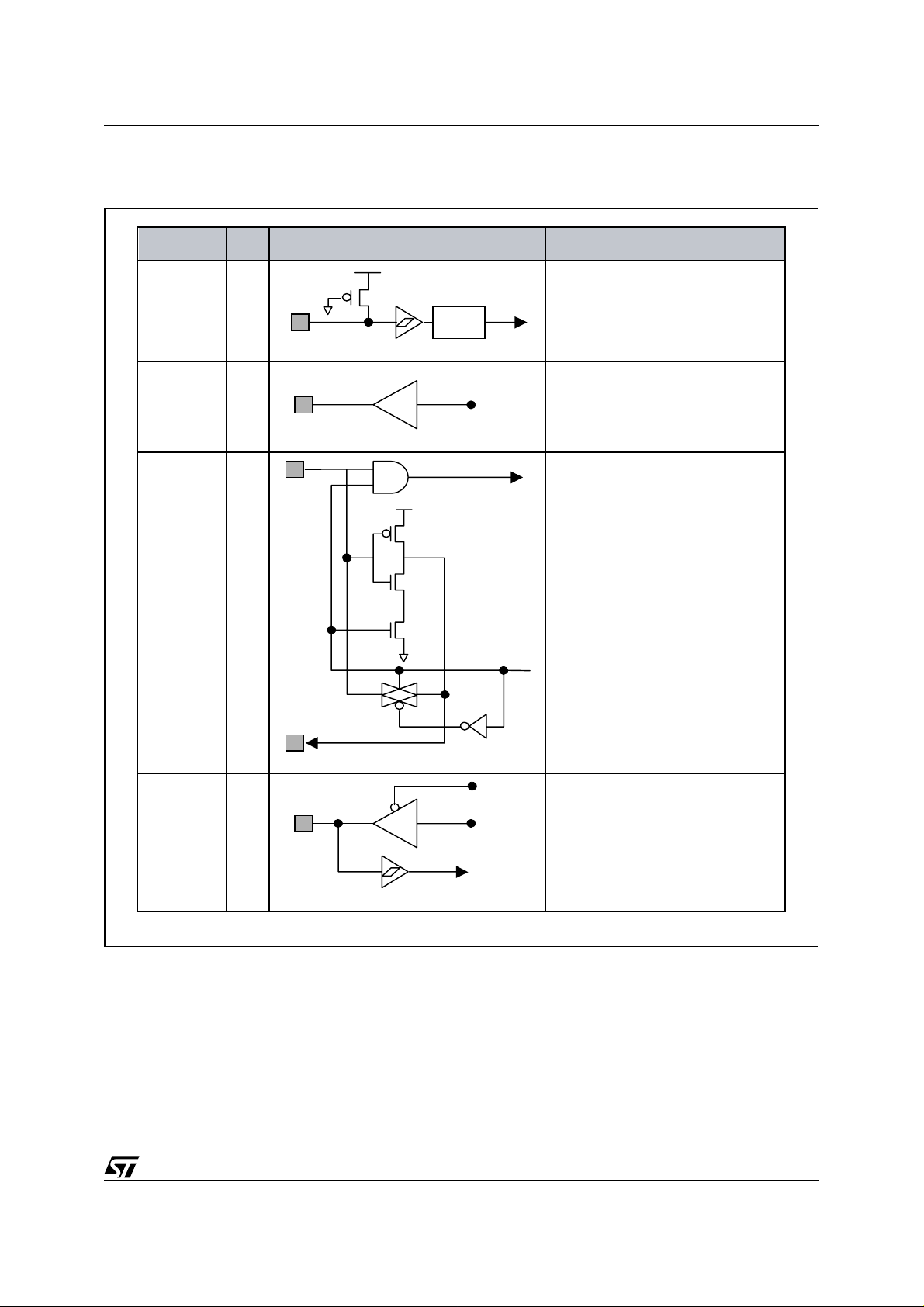
uPSD3234A, uPSD3234BV, uPSD3233B, uPSD3233BV
PORT Type and Descripti on
Figure 17. PORT Type and Description (Part 1)
Symbol Circuit Description
RESET I
WR, RD,ALE,
PSEN
XTAL1,
XTAL2
In /
Out
O
I
NFC
xon
• Schmitt input with internal pull-up
CMOS compatible interface
NFC : 400ns
Output only
On-chip oscillator
On-chip feedback resistor
Stop in the power down mode
External clock input available
CMOS compatible interface
O
PORT0 I/O
Bidirectional I/O port
Schmitt input
Address Output ( Push-Pull )
CMOS compatible interface
AI06653
43/170
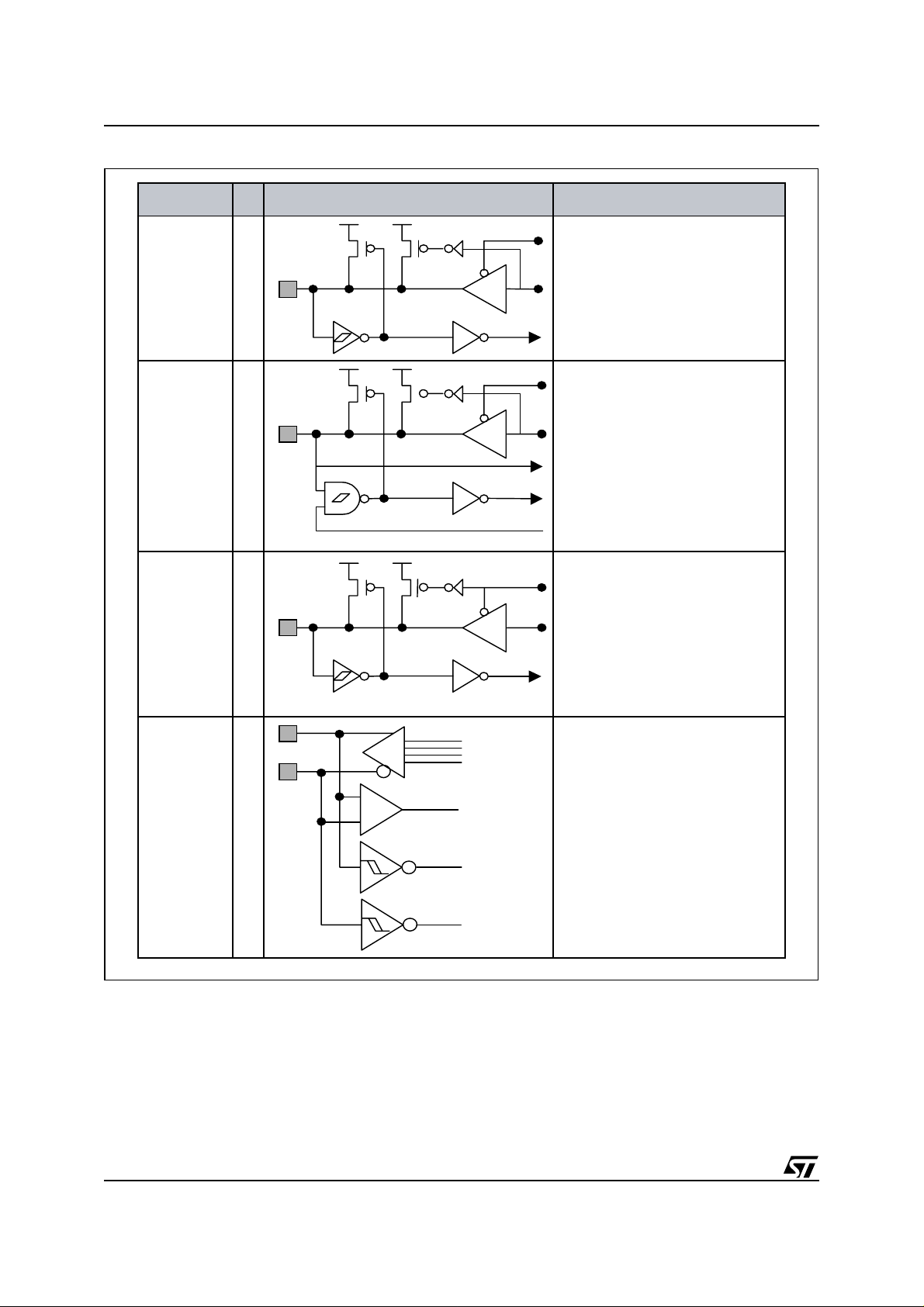
uPSD3234A, uPSD3234BV, uPSD3233B, uPSD3233BV
Figure 18. PORT Type and Description (Part 2)
Symbol Circuit Function
PORT1 <3:0>,
PORT3,
PORT4<7:3,1:0>
PORT2
PORT1 < 7:4 > I/O
PORT4.2
In/
Out
I/O
I/O
an_enb
Bidirectional I/O port with internal
pull-ups
Schmitt input
CMOS compatible interface
Bidirectional I/O port with internal
pull-ups
Schmitt input
CMOS compatible interface
Analog input option
Bidirectional I/O port with internal
pull-ups
Schmitt input.
TTL compatible interface
Pull-up when reset
Address Latch Enable
Program Strobe Enable
44/170
USB - ,
USB +
I/O
Bidirectional I/O port
Schmitt input
TTL compatible interface
+
–
AI06654

uPSD3234A, uPSD3234BV, uPSD3233B, uPSD3233BV
OSCILLATOR
The oscillator circuit of the uPS D323X D evices is
a single stage inverting amplifier in a Pierce oscillator configuration. The circuitry between XTAL1
and XTAL2 is basically an inverter biased t o the
transfer point. Either a crystal or ceramic resonator
can be used as the feedback element to complete
Figure 19. Oscillator
the oscillator circuit. Both are operated in parallel
resonance.
XTAL1 is the high gain amplifier input, and XTAL2
is the output. To drive the uPSD323X Devices externally, XTAL1 is driven from an external source
and XTAL2 left open-circuit.
XTAL1 XTAL2
8 to 40 MHz
SUPERVISORY
There are four ways to invoke a reset and initialize
the uPSD323X Devices.
■ Via the external RESET pin
■ Via the inter n al LVR Block .
■ Via USB bus reset signaling.
■ Via Watch Dog timer
Figure 20. RESET
Reset
Configuration
Noise
Cancel
WDT
XTAL1 XTAL2
External Clock
AI06620
The RESET
Each RESET
mechanism is illustrated in Figure 20.
source will cause a n internal reset
signal active. The CPU responds by executing an
internal reset and puts the internal registers in a
defined state. This internal reset is also routed as
an active low reset input to the PSD Module.
CPU
Clock
Sync
CPU
&
PERI.
LVR
RSTE
USB Reset
10ms
Timer
S
Q
R
10ms at 40Mhz
50ms at 8Mhz
PSD_RST
“Active Low
AI06621
45/170

uPSD3234A, uPSD3234BV, uPSD3233B, uPSD3233BV
External Reset
The RESET
for noise reduction. A RESET
holding the RESET
pin is connected to a Sc hmitt trigger
is accomplished by
pin LOW for at least 1ms at
power up while the oscillator is running. Refer to
AC spec on other RESET
Low V
Voltage Reset
DD
timing requirements.
An internal reset is generated by the LVR circuit
when the V
ter V
DD
the RESET
drops below the reset t hreshold. Af -
DD
reaching back up to the re set threshold,
signal will remain asserted for 10 ms
before it is released. On initial power-up the LVR
is enabled (default). After power-up the LVR can
be disabled via the LVREN Bit in the PCON Register.
Note: The LVR logic is still functio nal in both the
Idle and Power-down Modes.
The reset threshold:
■ 5V operation: 4V +/- 0.25V
■ 3.3V operation: 2.5V +/-0.2V
This logic supports approximately 0.1V of hysteresis and 1µs noise-cancelling delay.
Watchdog Timer Overflow
The Watchdog timer gene rates an internal reset
when its 22-bit counter overflows. See Watchdog
Timer section for details.
USB Reset
The USB reset is generated by a detection on t he
USB bus RESET
signal. A single-end zero on its
upstream port for 4 to 8 times will set RSTF Bit in
UISTA register. If Bit 6 (RSTE) of the UIEN Register is set, the detection will also generate the
RESET
signal to reset the CPU and other periph-
erals in the MCU.
46/170

uPSD3234A, uPSD3234BV, uPSD3233B, uPSD3233BV
WATCHDOG TIMER
The hardware watchdog timer (WDT) resets the
uPSD323X Devices when it overflows. The WDT
is intended as a recovery method in situations
where the CPU may be subject ed to a software
upset. To pr event a syste m reset the ti mer must be
reloaded in time by the application software. If the
processor suffers a hardware/software malfunction, the s oft wa re wi ll f ail to r elo ad th e t im er . T his
failure will result in a reset upon overflow thus preventing the processor running out of control.
In the Idle Mode the watchdog timer and reset circuitry remain active. The WDT consists of a 22-bit
counter, the Watchdog Timer RESET
SFR and Watchdog Key Register (WDKEY).
Since the WDT is automatically enab led whi le the
processor is running. the user only needs to be
concerned with servicing it.
The 22-bit counter overflows when it reaches
4194304 (3FFFFFH). The WDT increments once
every machine cycle.
This means the user must reset the WDT at least
every 4194304 machine cycles (1.258 seconds at
(WDRST)
40MHz). To reset the WDT the user must write a
value between 00-7EH to the WDRST register.
The value that is written to the WDRST is loaded
to the 7MSB of the 22 -bit count er. This al lows the
user to pre-loaded the counter to an initial value to
generate a flexible Watchdog time out period.
Writing a “00” to WDRST clears the counter.
The watchdog timer is controlled by the watchdog
key register, WDKEY. Only pattern 01010101
(=55H), disables the watchdog tim er. The rest of
pattern combinations will keep the watchdog timer
enabled. This security key will p reve nt the wa tchdog timer from being terminated abnormally when
the function of the watchdog timer is needed.
In Idle Mode, the oscillator continues to run. To
prevent the WDT from resetting the processor
while in Idle, the user should always set up a timer
that will periodically exit Idle, service the WDT, and
re-enter Idle Mode.
Watchdog reset pulse width depends on the clock
frequency. The reset period is Tf
The RESET
pulse width is Tf
OSC
x 12 x 222.
OSC
x 12 x 215.
Table 32. Watchdog Timer Key Register (WDKEY: 0AEH)
76543210
WDKEY7 WDKEY6 WDKEY5 WDKEY4 WDKEY3 WDKEY2 WDKEY1 WDKEY0
Table 33. Description of the WDKEY Bits
Bit Symbol Function
7 to 0
WDKEY7 to
WDKEY0
Enable or disable watchdog timer.
01010101 (=55h): disable watchdog timer. Others: enable watchdog timer
47/170
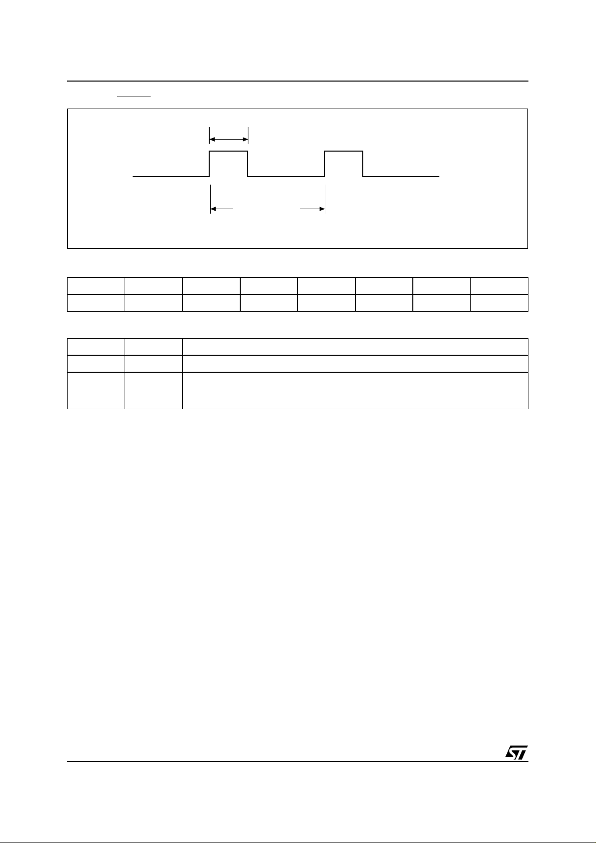
uPSD3234A, uPSD3234BV, uPSD3233B, uPSD3233BV
Figure 21. RESET Pulse Width
Reset pulse width (about 10ms at 40Mhz, about 50ms at 8Mhz)
Reset period
(1.258 second at 40Mhz)
(about 6.291 seconds at 8Mhz)
AI06823
Table 34. Watchdog Timer Clear Register (WDRST: 0A6H)
76543210
Reserved WDRST6 WDRST5 WDRST4 WDRST3 WDRST2 WDRST1 WDRST0
Table 35. Description of the WDRST Bits
Bit Symbol Function
7—Reserved
6 to 0
Note: The Watchdog Timer (WDT) is enabl ed at power-up or reset and m ust be served or disable d.
WDRST6 to
WDRST0
To reset watchdog timer, write any value beteen 00h and 7Eh to this register.
This value is loaded to the 7 most significant bits of the 22-bit counter.
For example: MOV WDRST,#1EH
48/170

uPSD3234A, uPSD3234BV, uPSD3233B, uPSD3233BV
TIMER/ COUNTERS (TIMER 0, TIMER 1 AND TIMER 2)
The uPSD323X Devices has three 16-bit Timer/
Counter registers: Timer 0, Timer 1 and Timer 2.
All of them can be confi gured to operate either as
timers or event counters and are compa tible with
standard 8032 architecture.
In the “Timer” function, the register is incremented
every machine cycle. Thus, one can think of it as
counting machine cycles. Since a machine cycle
consists of 6 CPU clock periods, the count rate is
1/6 of the CPU clock frequency or 1/12 o f the oscillator frequency (f
OSC
).
In the “Counter” function, the register is incremented in response to a 1-to-0 transition at its corresponding external input pin, T0 or T1. In this
function, the external input is sampled during
S5P2 of every machine cycle . When the sam ples
show a high in one cycle and a low in the next cycle, the count is incremented. The new count value
appears in the register during S3P1 of the cycle
Table 36. Control Register (TCON)
76543210
TF1 TR1 TF0 TR0 IE1 IT1 IE0 IT0
following the one in which the transition was detected. Since it takes 2 machine cycles (24 f
clock periods) to recognize a 1-to-0 transition, the
maximum count rate is 1/24 of the f
. There are
OSC
no restrictions on the duty cycl e of the extern a l input signal, but to ensure that a given level is sampled at least once before it changes , it should be
held for at least one full cycle. In addition to the
“Timer” or “Counter” selection, Timer 0 and Timer
1 have four operating modes from which to select.
Timer 0 and Tim er 1
The “Timer” or “Counter” function is selected by
control bits C/ T in the Special Function Register
TMOD. These Timer/Counters have four ope rating modes, which are selected by bit-pairs (M1,
M0) in TMOD. Modes 0, 1, and 2 are the same for
Timers/ Counters. Mode 3 is different. The four operating modes are de-scribed in the following text.
OSC
Table 37. Description of the TCON Bits
Bit Symbol Function
7TF1
6 TR1 Timer 1 Run Control Bit. Set/cleared by software to turn Timer/Counter on or off
5TF0
4 TR0 Timer 0 Run Control Bit. Set/cleared by software to turn Timer/Counter on or off
3IE1
2IT1
1IE0
0IT0
Timer 1 Overflow Flag. Set by hardware on Timer/Counter overflow. Cleared by
hardware when processor vectors to interrupt routine
Timer 0 Overflow Flag. Set by hardier on Timer/Counter overflow. Cleared by hardware
when processor vectors to interrupt routine
Interrupt 1 Edge Flag. Set by hardware when external interrupt edge detected. Cleared
when interrupt processed
Interrupt 1 Type Control Bit. Set/cleared by software to specify falling-edge/low-level
triggered external interrupt
Interrupt 0 Edge Flag. Set by hardware when external interrupt edge detected. Cleared
when interrupt processed
Interrupt 0 Type Control Bit. Set/cleared by software to specify falling-edge/low-level
triggered external interrupt
49/170

uPSD3234A, uPSD3234BV, uPSD3233B, uPSD3233BV
Mode 0. Putting either Timer into Mode 0 makes
it look like an 8048 Timer, which is an 8-bit Counter
with a divide-by-32 prescaler. Figure 22., page 51
shows the Mode 0 operation as it applies to
Timer1.
In this mode, the Timer register is configured as a
13-bit register. As the count rolls o ver from al l '1s'
to all '0s,' it sets the Timer Interrupt Flag TF1. The
counted input is enabled to the Timer when TR1 =
1 and either GATE = 0 or /INT1 = 1. (Setting GATE
= 1 allows the Timer to be controlled by external input /INT1, to facilitate pulse width measurements).
The 13-bit register consists of all 8 bits of TH1 and
the lower 5 bits of TL1. The upper 3 bits of TL1 are
indeterminate and shou ld be ignored. Set ting the
run flag does not clear the registers.
Mode 0 operation is the same for the Timer0 as for
Timer1. Substitute TR0, TF0, and /INT0 for the
corresponding Timer1 signals in Figure
22., page 51. There are two different GATE Bits,
one for Timer1 and one for Timer0.
Mode 1. Mode 1 is the same as Mode 0, except
that the Timer register is being run with all 16 bits.
TR1 is a control bit in the Special Function Register TCON (TCON Control Register). GATE is in
TMOD.
Table 38. TMOD Register (TMOD)
76543210
Gate C/T
M1 M0 Gate C/T M1 M0
Table 39. Description of the TMOD Bits
Bit Symbol Timer Function
7Gate
Gating control when set. Timer/Counter 1 is enabled only while INT1 pin is High and
TR1 control pin is set. When cleared, Timer 1 is enabled whenever TR1 control bit is set
6C/T
5 M1 (M1,M0)=(0,0): 13-bit Timer/Counter, TH1, with TL1 as 5-bit prescaler
4M0
3Gate
2C/T
1 M1 (M1,M0)=(0,0): 13-bit Timer/Counter, TH0, with TL0 as 5-bit prescaler
0M0
Timer 1
Timer 0
Timer or Counter selector, cleared for timer operation (input from internal system clock);
set for counter operation (input from T1 input pin)
(M1,M0)=(0,1): 16-bit Timer/Counter. TH1 and TL1 are cascaded. There is no prescaler.
(M1,M0)=(1,0): 8-bit auto-reload Timer/Counter. TH1 holds a value which is to be
reloaded into TL1 each time it overflows
(M1,M0)=(1,1): Timer/Counter 1 stopped
Gating control when set. Timer/Counter 0 is enabled only while INT0 pin is High and
TR0 control pin is set. When cleared, Timer 0 is enabled whenever TR0 control bit is set
Timer or Counter selector, cleared for timer operation (input from internal system clock);
set for counter operation (input from T0 input pin)
(M1,M0)=(0,1): 16-bit Timer/Counter. TH0 and TL0 are cascaded. There is no prescaler.
(M1,M0)=(1,0): 8-bit auto-reload Timer/Counter. TH0 holds a value which is to be
reloaded into TL0 each time it overflows
(M1,M0)=(1,1): TL0 is an 8-bit Timer/Counter controlled by the standard TImer 0 control
bits. TH0 is an 8-bit timer only controlled by Timer 1 control bits
50/170

uPSD3234A, uPSD3234BV, uPSD3233B, uPSD3233BV
Figure 22. Ti m er/Counter Mode 0: 13 -bit Co unter
Gate
INT1 pin
f
OSC
T1 pin
TR1
÷ 12
C/T = 0
C/T = 1
Control
Figure 23. Timer/Counter Mode 2: 8-bit Auto-reload
f
OSC
T1 pin
TR1
÷ 12
C/T = 0
C/T = 1
Control
TL1
(5 bits)
TL1
(8 bits)
TH1
(8 bits)
TF1 Interrupt
AI06622
TF1 Interrupt
Gate
INT1 pin
TH1
(8 bits)
AI06623
51/170

uPSD3234A, uPSD3234BV, uPSD3233B, uPSD3233BV
Figure 24. Timer/Counter Mode 3: Two 8-bit Counters
Gate
INT0 pin
f
OSC
T0 pin
f
OSC
TR0
÷ 12
÷ 12
C/T = 0
C/T = 1
TR1
Control
Control
TL0
(8 bits)
TH1
(8 bits)
TF0 Interrupt
TF1 Interrupt
AI06624
52/170

uPSD3234A, uPSD3234BV, uPSD3233B, uPSD3233BV
Mode 2. Mode 2 configures the T im er register as
an 8-bit Counter (TL1) with a utomatic reload, as
shown in Figure 23., page 51. Overflow from TL1
not only sets TF1, but also reloads T L1 with the
contents of TH1, which is preset by software. The
reload leaves TH1 unchanged. Mode 2 operation
is the same for Timer/Counter 0.
Mode 3. Timer 1 in Mode 3 simply holds its count.
The effect is the same as setting TR1 = 0.
Timer 0 in Mode 3 establishes TL0 and TH0 as two
separate counters. The logic for Mode 3 on Timer
0 is shown in Figure 24 ., p age 52. TL0 uses the
Timer 0 c ontrol B its: C/T , GATE, TR0, IN T0, an d
TF0. TH0 is locked into a timer funct ion (co unting
machine cycles) and takes over the use of TR1
and TF1 from Timer 1. Thus, TH0 now controls the
“Timer 1“ Interrupt.
Mode 3 is provided for app lications requiring an
extra 8-bit timer on the counter. With Timer 0 in
Mode 3, an uPSD323X Devices can look like it has
three Timer/Counters. When Timer 0 is in Mode 3,
Timer 1 can be turned on and off by switching it out
of and into its own Mode 3, or can still be used by
the serial port as a baud rate generator, or in fact,
in any application not requiring an interrupt.
Timer 2
Like Timers 0 and 1, Timer 2 can operate as either
an event timer or as an event counter. This is selected by Bit C/T2 in the special function register
T2CON. It has three operating modes: capture,
autoload, and baud rate generator, which are se-
lected by bits in the T2CON as shown in Table
41., page 54. In the Capture M ode there are two
options which are selected by Bit EXEN2 in
T2CON. if EXEN2 = 0, then Timer 2 is a 16-bit timer or counter which upon overflowing sets Bit TF2,
the Timer 2 Overf low Bit, which can b e used to
generate an interrupt. If EXEN 2 = 1, then Timer 2
still does the above, but with the added feature
that a 1-to-0 transition at external input T2EX
causes the current value in the Timer 2 registers,
TL2 and TH2, to be captured into registers
RCAP2L and RCAP2H, respectively. In addition,
the transition at T2EX causes Bit EXF2 in T2CON
to be set, and EXF2 like TF2 c an generate an interrupt. The Cap ture Mode is illu strated in Figure
25., page 55.
In the Auto-reload Mode, there are again two options, wh ich are s e lected by bi t EXEN2 in T2CON.
If EXEN2 = 0, then when Timer 2 rolls over it not
only sets TF2 but a lso causes th e Timer 2 registers to be reloaded with the 16-bit value in registers RCAP2L and RCAP2H, which are preset by
software. If EXEN2 = 1, then Timer 2 still does the
above, but with the added feature that a 1-to-0
transition at external input T2EX will also trigger
the 16-bit reload and set EXF2. The Auto-reload
Mode is illustrated in Standard Serial Interface
(UART) Figure 26., page 55. The Baud Rate Generation Mode is selected by (RCLK, RCLK1)=1
and/or (TCLK, TCLK1)=1. It will be described in
conjunction with the serial port.
Table 40. Timer/Counter 2 Control Register (T2CON)
76543210
TF2 EXF2 RCLK TCLK EXEN2 TR2 C/T
2CP/RL2
53/170

uPSD3234A, uPSD3234BV, uPSD3233B, uPSD3233BV
Table 41. Description of the T2CON Bits
Bit Symbol Function
7TF2
Timer 2 overflow flag. Set by a Timer 2 overflow, and must be cleared by software. TF2
will not be set when either (RCLK, RCLK1)=1 or (TCLK, TCLK)=1
Timer 2 external flag set when either a capture or reload is caused by a negative
6EXF2
transition on T2EX and EXEN2=1. When Timer 2 Interrupt is enabled, EXF2=1 will
cause the CPU to vector to the Timer 2 Interrupt routine. EXF2 must be cleared by
software
Receive clock flag (UART 1). When set, causes the serial port to use Timer 2 overflow
(1)
5
RCLK
pulses for its receive clock in Modes 1 and 3. TCLK=0 causes Timer 1 overflow to be
used for the receive clock
Transmit clock flag (UART 1). When set, causes the serial port to use Timer 2 overflow
(1)
4
TCLK
pulses for its transmit clock in Modes 1 and 3. TCLK=0 causes Timer 1 overflow to be
used for the transmit clock
Timer 2 external enable flag. When set, allows a capture or reload to occur as a result of
3 EXEN2
a negative transition on T2EX if Timer 2 is not being used to clock the serial port.
EXEN2=0 causes Time 2 to ignore events at T2EX
2 TR2 Start/stop control for Timer 2. A logic 1 starts the timer
Timer or Counter select for Timer 2. Cleared for timer operation (input from internal
1C/T
2
system clock, t
); set for external event counter operation (negative edge triggered)
CPU
Capture/reload flag. When set, capture will occur on negative transition of T2EX if
EXEN2=1. When cleared, auto-reload will occur either with TImer 2 overflows, or
0CP/RL
2
negative transitions of T2EX when EXEN2=1. When either (RCLK, RCLK1)=1 or (TCLK,
TCLK)=1, this bit is ignored, and timer is forced to auto-reload on Timer 2 overflow
Note: 1. The RCLK1 a nd TCLK1 Bits i n the PCON Regi ster control UART 2, and have the same f unction as RC LK and TCLK.
Table 42. Timer/Counter2 Op erating Mod es
T2CON
Mode
RxCLK
or
TxCLK
CP/
RL
T2MOD
TR2 Internal
2
DECN
T2CON
EXEN
P1.1
T2EX
Remarks
0 0 1 0 0 x reload upon overflow
16-bit
0010 1↓ reload trigger (falling edge)
Auto-
reload
0 0 1 1 x 0 Down counting
0 0 1 1 x 1 Up counting
16-bit
011x 0x
Capture
011x 1↓
1x1x 0x
Baud Rate
Generator
1x1x 1↓
16-bit Timer/Counter
(only up counting)
Capture (TH1,TL2) →
(RCAP2H,RCAP2L)
No overflow interrupt
request (TF2)
Extra External Interrupt
(Timer 2)
Off x x 0 x x x Timer 2 stops — —
Note: ↓ = falling edge
Input Clock
/12
f
OSC
/12
f
OSC
/12
f
OSC
External
(P1.0/T2)
MAX
/24
f
OSC
MAX
/24
f
OSC
MAX
/24
f
OSC
54/170

Figure 25. Tim er 2 in Cap t ure Mode
uPSD3234A, uPSD3234BV, uPSD3233B, uPSD3233BV
f
OSC
T2 pin
T2EX pin
÷ 12
Transition
Detector
C/T2 = 0
C/T2 = 1
TR2
EXEN2
Control
Capture
Control
Figure 26. Tim er 2 in Aut o- Re l oad Mode
TL2
(8 bits)
RCAP2L
TH2
(8 bits)
RCAP2H
TF2
Timer 2
Interrupt
EXP2
AI06625
f
OSC
T2 pin
T2EX pin
÷ 12
Transition
Detector
C/T2 = 0
C/T2 = 1
TR2
EXEN2
Control
Reload
Control
TL2
(8 bits)
RCAP2L
TH2
(8 bits)
RCAP2H
TF2
Timer 2
Interrupt
EXP2
AI06626
55/170

uPSD3234A, uPSD3234BV, uPSD3233B, uPSD3233BV
STANDARD SERIAL INTERFACE (UART)
The uPSD323X Devices provides two standard
8032 UART serial ports. The first port is connected
to pin P3.0 (RX) and P3.1 (TX). The second port is
connected to pin P1.2 (RX) and P1.3(TX). The operation of the two serial ports are the same and are
controlled by the SCON and SCON2 registers.
The serial port is full duplex, meaning it can transmit and receive simultaneously. It is also receivebuffered, meaning it can commence reception of a
second byte before a previously received byte has
been read from the register. (However, if the first
byte still has not been read by the time reception
of the second byte is complete, one of the bytes
will be lost.) The serial port receive and transmit
registers are both accessed at Special Function
Register SBUF (or SBUF2 for the second serial
port). Writing to SBUF load s the t rans mit registe r,
and reading SBUF accesses a physically separate
receive register.
The serial port can operate in 4 modes:
Mode 0. Serial data enters and exits through
RxD. TxD outputs the shift clock. 8 bits are transmitted/received (LSB first). The b aud rate is fixed
at 1/12 the f
OSC
.
Mode 1. 10 bits are transmitte d (through TxD) or
received (through RxD): a start Bit (0), 8 data bits
(LSB first), and a Stop Bit (1). On receive, the Stop
Bit goes into RB8 in Special Function Register
SCON. The baud rate is variable.
Mode 2. 11 bits are transmitte d (through TxD) or
received (through RxD): start Bit (0), 8 data bits
(LSB first), a programmable 9th data bit, and a
Stop Bit (1). On Transmit, the 9th data bit (TB8 in
SCON) can be assigned the value of '0' or '1. ' O r,
for example, the Parity Bit (P, in the PSW) could
be moved into TB8. O n receive, the 9th data bit
goes into RB8 in Special Function Register SCON,
while the Stop Bit is ignored. The baud rate is programmable to either 1/32 or 1/64 the oscillator frequency.
Mode 3. 11 bits are transmitte d (through TxD) or
received (through RxD): a start Bit (0), 8 data bits
(LSB first), a programmable 9th data bit, and a
Stop Bit (1). In fact, Mode 3 is the same as Mode
2 in all respects except baud rate. Th e baud rate
in Mode 3 i s variable.
In all four modes, transmission is initiated by any
instruction that uses SBUF as a d estin ation register. Reception is initiated in Mode 0 by the co ndition RI = 0 and REN = 1. Reception is initiated in
the other modes by the incoming start bit if REN =
1.
Multiprocessor Communications
Modes 2 and 3 have a special provision for m ultiprocessor communications. In these modes, 9
data bits are received. The 9th one goes into RB8.
Then comes a Stop Bit. The port can be programmed such that when the Stop Bit is received,
the serial port interrupt will be activated only if RB8
= 1. This feature is enabled by setting Bit SM2 in
SCON. A way to use this feature in mul ti-processor systems is as follows:
When the master processor wants to transmit a
block of data to one of several slaves, it first sends
out an address byte which identifies the target
slave. An address byte differs from a data by te in
that the 9th bit is '1' in an ad dres s by te and 0 in a
data byte. With SM2 = 1, no slave will be interrupted by a data byte. An ad-dress byte, however, will
interrupt all slaves, so that e ach slave can e xamine the received byte and see if it is being addressed. The addressed slave will clear its SM2
Bit and prepare to receive the d ata bytes that wi ll
be coming. The slaves that weren’t being addressed leave their SM2s set and go on about
their business, ignoring the coming data bytes.
SM2 has no ef fect in Mode 0, and in Mode 1 can
be used to check the validity of the Stop B it. In a
Mode 1 reception, if SM2 = 1, the receive interrupt
will not be activ ated un less a valid S top Bit is received.
Serial Port Control Register
The serial port control and status register is the
Special Function Register SCON (SCON2 for the
second port), shown in Figure 27. , page 61. This
register contains not only the mode s el ection bit s,
but also the 9th data bit for transmit and receive
(TB8 and RB8), and the Serial Port Interrupt Bits
(TI and RI).
Table 43. Serial Port Control Register (SCON)
76543210
SM0 SM1 SM2 REN TB8 RB8 TI RI
56/170

uPSD3234A, uPSD3234BV, uPSD3233B, uPSD3233BV
Table 44. Description of the SCON Bits
Bit Symbol Function
7 SM0 (SM1,SM0)=(0,0): Shift Register. Baud rate = f
(SM1,SM0)=(1,0): 8-bit UART. Baud rate = variable
6SM1
5SM2
4REN
3TB8
2RB8
1TI
0RI
(SM1,SM0)=(0,1): 8-bit UART. Baud rate = f
(SM1,SM0)=(1,1): 8-bit UART. Baud rate = variable
Enables the multiprocessor communication features in Mode 2 and 3. In Mode 2 or 3, if
SM2 is set to '1,' RI will not be activated if its received 8th data bit (RB8) is '0.' In Mode 1,
if SM2=1, RI will not be activated if a valid Stop Bit was not received. In Mode 0, SM2
should be '0'
Enables serial reception. Set by software to enable reception. Clear by software to
disable reception
The 8th data bit that will be transmitted in Modes 2 and 3. Set or clear by software as
desired
In Modes 2 and 3, this bit contains the 8th data bit that was received. In Mode 1, if
SM2=0, RB8 is the Snap Bit that was received. In Mode 0, RB8 is not used
Transmit Interrupt Flag. Set by hardware at the end of the 8th bit time in Mode 0, or at
the beginning of the Stop Bit in the other modes, in any serial transmission. Must be
cleared by software
Receive Interrupt Flag. Set by hardware at the end of the 8th bit time in Mode 0, or
halfway through the Stop Bit in the other modes, in any serial reception (except for
SM2). Must be cleared by software
Baud Rates. T he baud rate in Mode 0 is fixed:
Mode 0 Baud Rate = f
OSC
/ 12
The baud rate in Mode 2 depends on the value of
Bit SMOD = 0 (whi ch is the value on reset), t he
baud rate is 1/64 the oscillator frequency. If SMOD
= 1, the baud rate is 1/32 the oscillator frequency.
SMOD
Mode 2 Baud Rate = (2
/ 64) x f
OSC
In the uPSD323X Devices, the baud rates in
Modes 1 and 3 are determined by the Timer 1
overflow rate.
Using Timer 1 to Generate Baud Ra tes . When
Timer 1 is used as the baud rate generator, the
baud rates in Modes 1 and 3 a re determined by
the Timer 1 overflow rate and the value of SMOD
as follows (see:
Mode 1,3 Baud Rate =
SMOD
(2
/ 32) x (Timer 1 overflow rate)
The Timer 1 Interrupt should be di sabled in this
application. The Timer itself can be conf igured for
either “timer” or “counter” operation, and in any of
its 3 running modes. In the m ost typical applications, it is configured for “timer” operation, in the
Auto-reload Mode (high nibble of TMOD = 0010B).
In that case the baud rate is given by the formula:
Mode 1,3 Baud Rate =
SMOD
(2
/ 32) x (f
/ (12 x [256 – (TH1)]))
OSC
/12
OSC
OSC
/64 or f
OSC
/32
One can achieve very low baud rates with Timer 1
by leaving the Timer 1 Interrupt enabled, and configuring the Timer to run as a 16-bit timer (hi gh nibble of TMOD = 0001B), and using the Timer 1
Interrupt to do a 16-bit software reload. Figure
22., page 51 lists various commonly used baud
rates and how they can be obtained from Timer 1.
Using Timer/Counter 2 to Generate Baud
Rates. In the uPSD323X Devices, Timer 2 select-
ed as the baud rate generator by setting TCLK
and/or RCLK (see Figure 22., page 51 Timer/
Counter 2 Control Register (T2CON)).
Note: The baud rate for transmit and receive can
be simultaneously different. Setting RCLK and/or
TCLK puts Timer into its Baud Rate Generator
Mode.
The RCLK and TCLK Bits in the T2CON register
configure UART 1. The RCLK1 and TCLK1 Bits in
the PCON register configure UART 2.
The Baud Rate Generator Mode is similar to the
Auto-reload Mode, in that a roll over in TH2 causes
the Timer 2 registers to be reloaded with the 16-bit
value in registers RCAP2H and RCAP2L, which
are preset by software.
Now, the baud rates in Modes 1 and 3 are determined at Timer 2’s overflow rate as follows:
Mode 1,3 Baud Rate = Timer 2 Overflow Rate / 16
57/170

uPSD3234A, uPSD3234BV, uPSD3233B, uPSD3233BV
Table 45. Timer 1-Generated Commonly Used Baud Rates
Baud Rate
Mode 0 Max: 1MHz 12MHz X X X X
Mode 2 Max: 375K 12MHz 1 X X X
Modes 1, 3: 62.5K 12MHz 1 0 2 FFh
19.2K 11.059MHz 1 0 2 FDh
9.6K 11.059MHz 0 0 2 FDh
4.8K 11.059MHz 0 0 2 FAh
2.4K 11.059MHz 0 0 2 F4h
1.2K 11.059MHz 0 0 2 E8h
137.5 11.059MHz 0 0 2 1Dh
110 6MHz 0 0 2 72h
110 12MHz 0 0 1 FEEBh
f
OSC
SMOD Timer 1
C/T Mode Reload Value
The timer can be configured for either “timer” or
“counter” operation. In the most typical applications, it is configured for “timer” operation (C/ T2 =
0). “Timer” operation is a little different for Timer 2
when it’s being used as a baud rate generator.
Normally, as a timer it would increment every machine cycle (thus at the 1/6 the CPU clock frequency). In the case, the baud rate is given by the
formula:
Mode 1,3 Baud Rate =
/ (32 x [65536 – (RCAP2H, RCAP2L)]
f
OSC
where (RCAP2H, RCAP2L) is the content of
RC2H and RC2L taken as a 16-bit unsigned integer.
Timer 2 also be used as the Baud Rate Generating
Mode. This mode is valid only if RCLK + TCLK = 1
in T2CON or in PCON.
Note: A roll-over in TH2 does not set TF2, and will
not generate an interrupt. Therefore, the Timer Interrupt does not have to be disabled when Timer 2
is in the Baud Rate Generator Mode.
Note: If EXEN2 is set, a 1-to-0 transition in T2EX
will set EXF2 but will not cause a reload from
(RCAP2H, RCAP2L) to (TH2, TL2). Thus when
Timer 2 is in use as a baud rate gene rator, T2EX
can be used as an extra external interrupt, if desired.
It should be noted that when Timer 2 is running
(TR2 = 1) in “timer” function in the Baud Rate Generator Mode, one should not try to READ or
WRITE TH2 or TL2. Un der these conditions the
timer is being incremented every state time, and
the results of a READ or WRITE may not be accurate. The RC registers may be read, but should not
be written to, because a WRITE might overlap a
reload and cause WRITE and/or reload errors.
Turn the timer off (clear TR2) before accessing the
Timer 2 or RC registers, in this case.
More Abo ut Mode 0. Serial data enters and exits
through RxD. TxD outputs the shift clock. 8 bits are
transmitted/received: 8 data bits (LS B first). The
baud rate is fixed at 1/12 the f
OSC
.
Figure 27., page 61 shows a simplified functional
diagram of the serial port in Mode 0, and associated timing.
Transmission is initiated by any instruction that
uses SBUF as a destination register. The “WRITE
to SBUF” signal at S6P2 also loads a '1' into the
9th position of the trans mit shift register and tells
the TX Control block to commence a transmission.
The internal timing is such that one f ull machine
cycle will e lapse be tween “WR ITE to SBUF ” and
activation of SEND.
SEND enables the output of the shift register to the
alternate out-put function line of RxD and also enable SHIFT CLOCK to the alternate output function line o f TxD. SH IFT CLOC K is lo w during S3,
S4, and S5 of every mac hine cycle , and hig h during S6, S1, and S2. At S6P2 of every machine cycle in which SEND is active, the contents of t he
transmit shift are shifted to the right one position.
58/170

uPSD3234A, uPSD3234BV, uPSD3233B, uPSD3233BV
As data bits shift out to the right, zeros come in
from the left. When the MS B o f the da ta b yte is at
the output position of the shift register, then the '1'
that was initially loaded into the 9th position, is just
to the left of the MSB, and all positions to the left
of that contain zeros. This condition flags the TX
Control block to do one last shift and then dea ctivate SEND and set T1. Both of these actions occur
at S1P1. Both of these actions occur at S1P1 of
the 10th machine cycle after “WRITE to SBUF.”
Reception is initiated by the condition REN = 1 and
R1 = 0. At S6P2 of the next machi ne cycl e, the RX
Control unit writes the bits 11111110 to the receive
shift register, and in the next clock phase activates
RECEIVE.
RECEIVE enables SHIFT CLOCK to the alternate
output function line of TxD. SHIFT CLOCK makes
transitions at S3P1 and S6P1 of every machine
cycle in which RECEIVE is ac tive, the conten ts of
the receive shift register are shifted to the left one
position. The value that com es in from the right is
the value that was sampled at the RxD pin at S5P2
of the same machine cycle.
As data bits come in from the right, '1s' shift out to
the left. When the '0' that was initially loaded into
the right-most position arrives at the left-most position in the shift register, it flags the RX Control
block to do one last shift and load SBUF. At S1P1
of the 10th machine cycle after the WRITE to
SCON that cleared RI, RECEIVE is cleared as RI
is set.
More Abo ut Mode 1. Ten bits are transmitted
(through TxD), or received (through RxD): a start
Bit (0), 8 data bits (LSB first). and a Stop Bit (1). On
receive, the Stop Bit goes into RB8 in SCON. In
the uPSD323X Devices the baud rate is determined by the Timer 1 or Timer 2 over-flow rate.
Figure 29., page 62 shows a simplified functional
diagram of the serial port in Mode 1, and associated timings for transmit receive.
Transmission is initiated by any instruction that
uses SBUF as a destination register. The “WRITE
to SBUF” signal also loads a '1' into the 9th bit position of the transmit shift register and flags the TX
Control unit that a transmission is requested.
Transmission actually commenc es at S1P1 of the
machine cycle following the next rollover in the divide-by-16 counter. (Thus, the bit times are synchronized to the divide-by-16 counter, not to the
“WRITE to SBUF” signal.)
The transmission beg ins with activation of SE ND
which puts the start bit at TxD. One bit time l ater,
DATA is activated, which enables the output bit of
the transmit shift register to TxD. The first shift
pulse occurs one bit time after that.
As data bits shift out to the right, zeros are clocked
in from the left. When the M SB o f the data byte is
at the output position of the shift register, then the
'1' that was initially loaded into the 9th pos ition is
just to the left of the MSB, and all positions to the
left of that contain zeros. This condition flags the
TX Control unit to do one last shift and then deactivate SEND and set TI. This occurs at t he 10th divide-by-16 rollover after “WRITE to SBUF.”
Reception is initiated by a detected 1-to-0 transition at RxD. For this purpose RxD is sampled at a
rate of 16 times what ever baud rate has bee n es tablished. When a transition is detected, the divide-by-16 counter is immediately reset, and 1FFH
is written into the input shift register. Resetting the
divide-by-16 counter aligns its roll-overs with the
boundaries of the incoming bit times.
The 16 states of the counter divide each bit time
into 16ths. At the 7 th, 8th, an d 9th counter sta tes
of each bit time, the bit detector samples the value
of RxD. The value accepted is the value that was
seen in at least 2 of the 3 samples. This is done for
noise rejection. If the value accepted during the
first bit time is not '0,' the receive circuits are reset
and the unit goes back to looking for an-other 1-to0 transition. This is to provide rejection of false
start bits. If the start bit proves valid, it is shifted
into the input shift register, and reception of the reset of the rest of the frame will proceed.
As data bits come in from the right, '1s' shift out to
the left. When the start bit arrives at the left-most
position in the shift register (which in Mode 1 is a
9-bit register), it flags the RX Control block to do
one last shift, load SBUF and RB8, and set RI. The
signal to load SBUF and RB8, and to set RI, will be
generated if, and only if, the following conditions
are met at the time the final shift pulse is generated:
1. R1 = 0, and
2. E ither S M2 = 0, or the received Stop Bit = 1.
If either of these two conditions is not m et, the re-
ceived frame is irretrievably lost. If both conditions
are met, the Stop Bit goes into RB8, the 8 data bits
go into SBUF, and RI is activated. At this time,
whether the above condi tions are met or not, the
unit goes back to looking for a 1-to-0 tr ansition in
RxD.
59/170

uPSD3234A, uPSD3234BV, uPSD3233B, uPSD3233BV
More About Modes 2 and 3. Eleven bits are
transmitted (through TxD), or received (through
RxD): a Start Bit (0), 8 data bits (LS B first), a programmable 9th data bit, and a Stop Bit (1). On
transmit, the 9th data b it (TB8) can be assigned
the value of '0' or '1.' On receive, the data bit goes
into RB8 in SCON. The baud rate is programmable to either 1/16 or 1/32 the CPU clock frequency
in Mode 2. Mode 3 may have a variable baud rate
generated from Timer 1.
Figure 31., page 63 and Figure 33., page 64 show
a functional diagram of the seria l port in Mo des 2
and 3. The receive portion is exactly the same as
in Mode 1. The transmit portion differs from M ode
1 only in the 9th bit of the transmit shift register.
Transmission is initiated by any instruction that
uses SBUF as a destination register. The “WRITE
to SBUF” signal also loads TB8 into the 9th bit position of the transmit shift register and flags the TX
Control unit that a transmission is requested.
Transmission commences at S1P1 of the machine
cycle following the next roll-over i n the divide-by16 counter. (Thus, the bit t imes are synchronized
to the divide-by-16 counter, not to the “WRITE to
SBUF” signal.)
The transmission begins with activation of S END,
which puts the start bit at TxD. One bit time l ater,
DATA is activated, which enables the output bit of
the transmit shift register to TxD. The first shift
pulse occurs one bit time after that. The first shift
clocks a '1' (the Stop Bit) into the 9th bit position of
the shift register. There-after, only zeros are
clocked in. Thus, as data bits shift out to the right,
zeros are clocked in from the l eft. When TB8 is at
the out-put position of the shift register, then the
Stop Bit is just to the left of TB8, and all positions
to the left of that contain zeros. This condition flags
the TX Control unit to do one last shift and then de-
activate SEND and set TI. This occurs at the 11th
divide-by 16 rollover after “WRITE to SUBF.”
Reception is initiated by a detected 1-to-0 transition at RxD. For this purpose RxD is sampled at a
rate of 16 times what ever baud rate has bee n es tablished. When a transition is detected, the divide-by-16 counter is immediately reset, and 1FFH
is written to the input shift register.
At the 7th, 8th, and 9th counter sta tes of each bit
time, the bit detector sam ples the value of R -D.
The value accepted is the value that was seen in
at least 2 of the 3 samples. If the value accepted
during the first bit time is not '0,' the receive circuits
are reset and the unit goes back to looking for another 1-to- 0 transition. I f th e S tart Bi t proves val id,
it is shifted into the input s hi ft register, and rec eption of the rest of the frame will proceed.
As data bits come in from the right, '1s' shift out to
the left. When the Start Bit arrives at the l eft-m ost
position in the shift register (which in Modes 2 and
3 is a 9-bit register), it flags the RX Control block
to do one last shift, load SBUF and RB8, and set
RI.
The signal to load SBUF a nd RB8, a nd to set RI,
will be generated if, and only if, the following conditions are met at th e time the final shift pul se is
generated:
1. RI = 0, and
2. Either SM2 = 0, or the received 9th data bit = 1
If either of these conditions is not met, the received
frame is irretrievably lost, and RI is not set. If both
conditions are met, the recei ve d 9th dat a bit goes
into RB8, and the first 8 data bits go into SBUF.
One bit time later, whether the above conditions
were met or not, the unit goes bac k to looking for
a 1-to-0 transition at the RxD input.
60/170

uPSD3234A, uPSD3234BV, uPSD3233B, uPSD3233BV
Figure 27. Serial Port Mode 0, Block Diagram
Internal Bus
Write
to
SBUF
DS
CL
Q
Zero Detector
SBUF
RxD
P3.0 Alt
Output
Function
Start
S6
REN
R1
Serial
Port
Interrupt
Tx Clock
Rx Clock
Start
Load
SBUF
Read
SBUF
Figure 28. Serial Port Mode 0, Waveforms
Write to SBUF
Send
Shift
RxD (Data Out)
TxD (Shift Clock)
S6P2
D0 D1 D2 D3 D4 D5 D6 D7
T
S3P1 S6P1
Tx Control
T
R
Rx Control
7 6 5 4 3 2 1 0
Input Shift Register
SBUF
Internal Bus
Send
Receive
Shift
Shift
Shift
Shift
Clock
RxD
P3.0 Alt
Input
Function
Transmit
TxD
P3.1 Alt
Output
Function
AI06824
Write to SCON
Receive
Shift
RxD (Data In)
TxD (Shift Clock)
RI
Clear RI
Receive
D0 D1 D2 D3 D4 D5 D6 D7
AI06825
61/170

uPSD3234A, uPSD3234BV, uPSD3233B, uPSD3233BV
Figure 29. Serial Port Mode 1, Block Diagram
Overflow
SMOD
TCLK
RCLK
Timer1
÷2
01
Overflow
01
0
1
Timer2
Write
to
SBUF
RxD
Sample
1-to-0
Transition
Detector
÷16
Serial
Port
Interrupt
Rx Detector
TB8
DS
CL
Q
Start
Tx Clock
÷16
Rx Clock
Start
Load
SBUF
Internal Bus
SBUF
Zero Detector
Tx Control
TI
RI
Rx Control
1FFh
Input Shift Register
Shift
Send
Load SBUF
TxD
Data
Shift
Shift
Figure 30. Serial Port Mode 1, Waveforms
Tx Clock
Write to SBUF
Send
Data
Shift
TxD
T1
Rx Clock
RxD
Bit Detector
Sample Times
Shift
RI
S1P1
Start Bit
÷16 Reset
Start Bit
D0 D1 D2 D3 D4 D5 D6 D7
D0 D1 D2 D3 D4 D5 D6 D7
Read
SBUF
SBUF
Internal Bus
Stop Bit
Stop Bit
AI06826
Transmit
Receive
AI06843
62/170
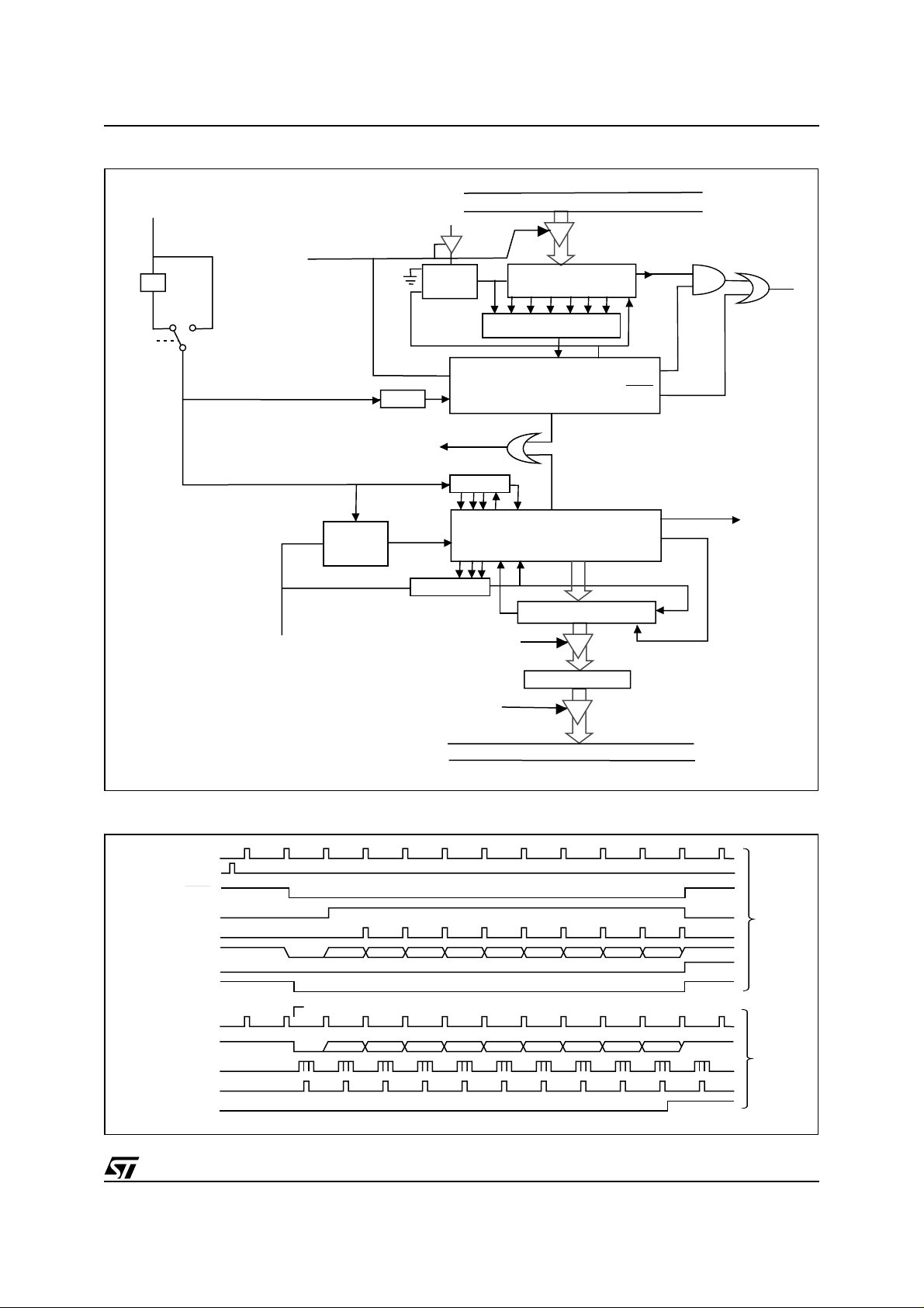
uPSD3234A, uPSD3234BV, uPSD3233B, uPSD3233BV
Figure 31. Serial Port Mode 2, Block Diagram
Phase2 Clock
1/2*f
OSC
÷2
SMOD
01
Write
to
SBUF
RxD
Sample
1-to-0
Transition
Detector
÷16
Serial
Port
Interrupt
Rx Detector
TB8
DS
CL
Q
Start
Tx Clock
÷16
Rx Clock
Start
Load
SBUF
Internal Bus
SBUF
Zero Detector
Tx Control
TI
RI
Rx Control
1FFh
Input Shift Register
Shift
Send
Load SBUF
TxD
Data
Shift
Shift
Figure 32. Serial Port Mode 2, Waveforms
Tx Clock
Write to SBUF
Send
Data
Shift
TxD
Stop Bit
Generator
Rx Clock
RxD
Bit Detector
Sample Times
Shift
TI
RI
S1P1
Start Bit
÷16 Reset
Start Bit
D0 D1 D2 D3 D4 D5 D6 D7
D0 D1 D2 D3 D4 D5 D6 D7
Read
SBUF
SBUF
Internal Bus
TB8
RB8
Stop Bit
Stop Bit
AI06844
Transmit
Receive
AI06845
63/170

uPSD3234A, uPSD3234BV, uPSD3233B, uPSD3233BV
Figure 33. Serial Port Mode 3, Block Diagram
Overflow
SMOD
TCLK
RCLK
Timer1
÷2
01
Overflow
01
0
1
Timer2
Write
to
SBUF
RxD
Sample
1-to-0
Transition
Detector
÷16
Serial
Port
Interrupt
Rx Detector
TB8
DS
CL
Q
Start
Tx Clock
÷16
Rx Clock
Start
Load
SBUF
Internal Bus
SBUF
Zero Detector
Tx Control
TI
RI
Rx Control
1FFh
Input Shift Register
Shift
Send
Load SBUF
TxD
Data
Shift
Shift
Figure 34. Serial Port Mode 3, Waveforms
Tx Clock
Write to SBUF
Send
Data
Shift
TxD
Stop Bit
Generator
Rx Clock
RxD
Bit Detector
Sample Times
Shift
TI
RI
S1P1
Start Bit
÷16 Reset
Start Bit
D0 D1 D2 D3 D4 D5 D6 D7
D0 D1 D2 D3 D4 D5 D6 D7
Read
SBUF
SBUF
Internal Bus
TB8
RB8
Stop Bit
Stop Bit
AI06846
Transmit
Receive
AI06847
64/170

uPSD3234A, uPSD3234BV, uPSD3233B, uPSD3233BV
ecode
ANALO G-TO-D IGITAL CONVER TOR (ADC)
The analog to digital (A/D) c onverter allows conversion of an analog input to a corresponding 8-bit
digital value. The A/D module has four analog inputs, which are multiplexed into one sample and
hold. The output of the sample and hold is the input into the converter, which generates the result
via successive approximation. The analog supply
voltage is connected to AV
of ladder resistance
REF
of A/D module.
The A/D module has two regi sters which are the
control register ACON and A/D result register
ADAT. The register ACON, shown in Table
47., page 66, controls the operation of the A/D
converter module. To use analog inputs, I/O is selected by P1SFS register. Also an 8-bit prescaler
ASCL divides the main system clock input down to
approximately 6MHz clock that is required f or the
ADC logic. Appropriate values need to be loaded
into the prescaler based upon the main MCU clock
frequency prior to use.
The processing of conversion starts when the
Start Bit ADST is set to '1.' After one cycle, it is
cleared by hardware. The register AD AT cont ains
the results of the A/D conversion. When conversion is completed, the result is loaded into the
ADAT the A/D Conversion Status Bit ADSF is set
to '1.'
The block diagram of the A/D module is shown in
Figure 35. The A/D Status Bit ADSF is set automatically when A/D conversion is completed,
cleared when A/D conversion is in process.
The ASCL should be loaded with a value that results in a clock rate of approximately 6MHz for the
ADC using the following formula:
ADC clock input = (f
value +1)
Where f
The conversion time f or the ADC can be c alculat-
ed as follows:
ADC Conversion Time = 8 clock * 8bits * (ADC
Clock) ~= 10.67usec (at 6MHz)
ADC Interrupt
The ADSF Bit in the ACON register is set to '1'
when the A/D conversion is complete. The status
bit can be driven by the MCU, or it can be configured to generate a falling e dge i nterrupt wh en the
conversion is complete.
The ADSF Interrupt is enabled by setting the ADSFINT Bit in the PCON register. Once the bit is set,
the external INT1 Interrupt is disabled and the
ADSF Interrupt takes over as INT1. INT1 must be
configured as if it is an edge interrupt input. The
INP1 pin (p3.3) is available for genera l I/O functions, or Timer1 gate control.
/ 2) / (Prescaler register
OSC
is the MCU clock input frequency
OSC
Figure 35. A/D Block Diagram
AVREF
ACH0
ACH1
ACH2
ACH3
ACON
Input
MUX
S/H
Ladder
Resistor
D
INTERNAL BUS
Successive
Approximation
Circuit
Conversion
Complete
Interrupt
ADAT
AI06627
65/170

uPSD3234A, uPSD3234BV, uPSD3233B, uPSD3233BV
Table 46. ADC SFR Memory Map
SFR
Addr
Reg
Name
95 ASCL 00
76543210
Bit Register Name
Reset
Value
Comments
8-bit
Prescaler for
ADC clock
96 ADAT ADAT7 ADAT6 ADAT5 ADAT4 ADAT3 ADAT 2 ADAT1 ADAT0 00
97 ACON ADEN ADS1 ADS0 ADST ADSF 00
Table 47. Description of the ACON Bits
Bit Symbol Function
7 to 6 — Reserved
5
4—Reserved
3 to 2
1
0
ADEN ADC Enable Bit: 0 : ADC shut off and consumes no operating current
1 : enable ADC
ADS1, ADS0 Analog channel select
0, 0
0, 1
1, 0
1, 1
ADST ADC Start Bit: 0 : force to zero
ADSF ADC Status Bit: 0 : A/D conversion is in process
Channel0 (ACH0)
Channel1 (ACH1)
Channel2 (ACH2)
Channel3 (ACH3)
1 : start an ADC; after one cycle, bit is cleared to '0'
1 : A/D conversion is completed, not in process
Table 48. ADC Clock Input
MCU Clock Frequency Prescaler Register Value ADC Clock
ADC Data
Register
ADC Control
Register
66/170
40MHz 2 6.7MHz
36MHz 2 6MHz
24MHz 1 6MHz
12MHz 0 6MHz

uPSD3234A, uPSD3234BV, uPSD3233B, uPSD3233BV
PULSE WIDTH MODULATION (PWM)
The PWM block has the following features:
■ Four-channel, 8-bit PWM unit with 16-bit
prescaler
■ One-channel, 8-bit unit with programmable
frequency and pulse width
■ PWM Output with programmable polarity
4-channel PWM Unit (PWM 0-3)
The 8-bit counter of a PWM counts modul e 256
(i.e., from 0 to 255, inclusive). The value held in
the 8-bit counter is compared to the contents of the
Special Function Register (PWM 0-3) of the corresponding PWM. T he pola rity of t he P WM o utputs
is programmable and selected by the PWML Bit in
PWMCON register. Provided the contents of a
PWM 0-3 register is greater than the counter value, the corresponding PWM output is set HIGH
(with PWML = 0). When the contents of this register is less than or equal to the counter value, the
corresponding PWM output is set LOW (with
PWML = 0). The pulse-width-ratio is therefore de-
Figure 36. Four-Channel 8-bit PWM Block Diagram
DATA BUS
fined by the contents of the corresponding Special
Function Register (PWM 0-3) o f a PWM . By loading the corresponding Spec ial Function Register
(PWM 0-3) with either 00H or FFH, the P WM output can be retained at a constant HIGH or LOW
level respectively (with PWML = 0).
For each PWM unit, there is a 16-bit Prescaler that
are used to divide the main system clock to form
the input clock for the corres ponding PWM unit.
This prescaler is used to define the desired repetition rate for the PWM unit. SFR registers B1h B2h are used to hold the 16-bit divisor values.
The repetition frequency of the PWM output is given by:
fPWM
8
= (f
/ prescaler0) / (2 x 256)
OSC
And the input clock frequency to the PWM
counters is = f
/ 2 / (prescaler data value + 1)
OSC
See I/O PORTS (MCU MODULE), page 42 for
more information on how to configure the Port 4
pin as PWM output.
f
OSC
CPU rd/wr
/2
8
CPU rd/wr
8
16-bit Prescaler
Register
(B2h,B1h)
16
16-bit Prescaler
Counter
8-bit PWM0-PWM3
8-bit PWM0-PWM3
Comparators Registers
8-bit PWM0-PWM3
clock
8
Data Registers
8
8
Comparators
8
8-bit Counter
Overflow
x 4
x 4
x 4
load
4
PWMCON bit7 (PWML)
Port4.3
Port4.4
Port4.5
Port4.6
load
PWMCON bit5 (PWME)
AI06647
67/170

uPSD3234A, uPSD3234BV, uPSD3233B, uPSD3233BV
Table 49. PWM SFR Memory Map
SFR
Reg Name
Addr
A1 PWMCON PWML PWMP PWME CFG4 CFG3 CFG2 CFG1 CFG0 00
76543210
Bit Register Name
Reset
Value
Comment
s
PWM
Control
Polarity
A2 PWM0 00
A3 PWM1 00
A4 PWM2 00
A5 PWM3 00
AA PWM4P 00
AB PWM4W 00
B1 PSCL0L 00
B2 PSCL0H 00
B3 PSCL1L 00
B4 PSCL1H 00
PWMCON Register Bit Definition:
– PWML = PWM 0-3 polarity control
– PWMP = PWM 4 polarity control
– PWME = PW M enable (0 = disabled, 1=
enabled)
– CFG3..CFG0 = PWM 0-3 Output (0 = Open
Drain; 1 = Push-Pull)
– CFG4 = PWM 4 Output (0 = Open Drain; 1 =
Push-Pull)
PWM0
Output
Duty Cycle
PWM1
Output
Duty Cycle
PWM2
Output
Duty Cycle
PWM3
Output
Duty Cycle
PWM 4
Period
PWM 4
Pulse
Width
Prescaler 0
Low (8-bit)
Prescaler 0
High (8-bit)
Prescaler 1
Low (8-bit)
Prescaler 1
High (8-bit)
68/170

uPSD3234A, uPSD3234BV, uPSD3233B, uPSD3233BV
Programm able Period 8-bi t PWM
The PWM 4 chan nel can be program med to provide a PWM output with variable pulse width and
period. The PWM 4 has a 16-bi t Prescaler, an 8bit Counter, a Pulse Width Register, a nd a Period
Register. The Pulse Width Register defines the
Figure 37. Programmable PWM 4 Channel Block Diagram
DATA BUS
8
PWM pulse width time, while the Period Regi ster
defines the period of the P WM . The input clock t o
the Prescaler is f
signed to Port 4.7.
8
/2. The PWM 4 channel is as-
OSC
8
f
OSC
CPU RD/WR
/ 2
PWMCON
Bit 5 (PWME)
8
16-bit Prescaler
Register
(B4h, B3h)
16
16-bit Prescaler
Counter
Load
CPU RD/WR
8-bit PWM4P
Register
(Period)
8
8-bit PWM4
Comparator
Register
8
8-bit PWM4
Comparator
88
PWM4
Control
Match
8-bit Counter
Clock
8-bit PWM4W
8-bit PWM4
Comparator
8-bit PWM4
Comparator
Reset
Register
(Width)
8
Load
Register
8
PWMCON
Bit 6 (PWMP)
Port 4.7
AI07091
69/170

uPSD3234A, uPSD3234BV, uPSD3233B, uPSD3233BV
PWM 4 Channel Operation
The 16-bit Prescaler1 divides the input clock
/2) to the desired frequency, the resulting
(f
OSC
clock runs the 8-bit Counter of the PWM 4 channel. The input clock frequency to the PWM 4
Counter is:
f PWM 4 = (f
/2)/(Prescaler1 data value +1)
OSC
When the Prescaler1 Register (B4h, B3h) is set to
data value '0,' the maximum input clock frequency
to the PWM 4 Counter is f
/2 and can be as high
OSC
as 20MHz.
The PWM 4 Counter is a free-running, 8-bit
counter. The output of the counter is compared t o
the Compare Registers, which are loaded with
data from the Pulse Width Register (PWM4W,
ABh) and the Period Register (PWM4P, AAh). The
Pulse Width Register defines the pulse duration or
the Pulse Width, while the Period Register defines
the period of the PWM. When the PWM 4 channel
is enabled, the register values are l oaded into the
Comparator Registers and are compared to the
Figure 38. PW M 4 Wit h P rogrammab le P ul se Wi dt h and Frequen cy
Counter output. When the content of the counter is
equal to or greater than the value in the Pulse
Width Register, it sets the PWM 4 output to low
(with PWMP Bit = 0). When the Period Register
equals to the PWM4 Counter, the Counter is
cleared, and the PWM 4 channel output is set to
logic 'high' level (beginning of the next PWM
pulse).
The Period Register cannot have a value of “00”
and its content should always be greater than the
Pulse Width Register.
The Prescaler1 Register, Pulse Width Register,
and Period Register can be modified while the
PWM 4 channel is active. The values of these registers are automatically loaded into the Prescaler
Counter and Comparator Registers when the current PWM 4 period ends.
The PWMCON Register (Bits 5 and 6) controls the
enable/disable and polarity of the PWM 4 channel.
PWM4
Defined by Pulse
Width Register
Defined by Period Register
Switch Level
RESET
Counter
AI07090
70/170

uPSD3234A, uPSD3234BV, uPSD3233B, uPSD3233BV
I2C INTERFAC E
There are two serial I2C ports impleme nted in t he
uPSD323X Devices.
The serial port supports the twin line I
sists of a data line (SDAx) and a clock line (SCLx).
Depending on the configuration, the SDA and SCL
lines may require pull-up resistors.
■ SDA1, SCL1: the serial port line for DDC
Protocol
■ SDA2, SCL2: the serial port line for general
2
C bus connection
I
2
In both I
C interfaces, these lines also function as
I/O port lines as follows.
■ SDA1 / P4.0, SCL 1 / P4.1 , SDA2 / P3. 6, SCL2
/ P3.7
The system is unique because data transport,
clock generation, address recognition and bus
control arbitration are all controlled by hardware.
Figure 39. Bl ock D i agram of the I
SDAx
2
C-bus, con-
2
C Bus Serial I/O
70
70
2
C serial I/O has complete autonomy in byte
The I
handling and operates in 4 modes.
■ Master transmitter
■ Master receiver
■ Slave transmitter
■ Slave receiver
These functions are controlled by the SFRs.
■ SxCON: the control of byte handling and the
operation of 4 mode.
■ SxSTA: the contents of its register may also
be used as a vector to various service
routines.
■ SxDAT: data shift register.
■ SxADR: slave address register. Slave address
recognition is performed by On-Chip H/W.
Slave Address
Shift Register
Internal Bus
AI06649
SCLx
Arbitration and Sync. Logic
Bus Clock Generator
70
Control Register
70
Status Register
Table 50. Serial Control Register (SxCON: S1CON, S2CON)
76543210
CR2 ENII STA STO ADDR AA CR1 CR0
71/170

uPSD3234A, uPSD3234BV, uPSD3233B, uPSD3233BV
Table 51. Description of the SxCON Bits
Bit Symbol Function
7CR2
6ENII
5STA
This bit along with Bits CR1and CR0 determines the serial clock frequency when SIO is
in the Master Mode.
Enable IIC. When ENI1 = 0, the IIC is disabled. SDA and SCL outputs are in the high
impedance state.
2
START flag. When this bit is set, the SIO H/W checks the status of the I
C-bus and
generates a START condition if the bus free. If the bus is busy, the SIO will generate a
repeated START condition when this bit is set.
STOP flag. With this bit set while in Master Mode a STOP condition is generated.
2
4STO
flag.
When a STOP condition is detected on the I
C-bus, the I2C hardware clears the STO
Note: This bit have to be set before 1 cycle interrupt period of STOP. That is, if this bit is
set, STOP condition in Master Mode is generated after 1 cycle interrupt period.
3 ADDR This bit is set when address byte was received. Must be cleared by software.
Acknowledge enable signal. If this bit is set, an acknowledge (low level to SDA) is
returned during the acknowledge clock pulse on the SCL line when:
• Own slave address is received
2AA
• A data byte is received while the device is programmed to be a Master Receiver
• A data byte is received while the device is a selected Slave Receiver. When this bit is
reset, no acknowledge is returned.
SIO release SDA line as high during the acknowledge clock pulse.
1CR1
0CR0
These two bits along with the CR2 Bit determine the serial clock frequency when SIO is
in the Master Mode.
Table 52. Selection of the Serial Clock Frequency SCL in Master Mode
Divisor
CR2 CR1 CR0
f
OSC
12MHz 24MHz 36MHz 40MHz
0 0 0 16 375 750 X X
0 0 1 24 250 500 750 833
0 1 0 30 200 400 600 666
0 1 1 60 100 200 300 333
1 0 0 120 50 100 150 166
1 0 1 240 25 50 75 83
1 1 0 480 12.5 25 37.5 41
1 1 1 960 6.25 12.5 18.75 20
Bit Rate (kHz) at f
OSC
72/170

uPSD3234A, uPSD3234BV, uPSD3233B, uPSD3233BV
Serial Status Register ( SxSTA : S1 STA, S2STA )
SxSTA is a “Read-only” register. The contents of
this register may be used as a vector to a service
routine. This optimized the response time o f the
software and consequently that of the I
The status codes for all possible modes of the I
2
C-bus.
2
C-
bus interface are given Table 54.
This flag is set, and an interrupt is generated, after
any of the following events occur.
1. Own slave address has been received during
AA = 1: ack_int
2. T he general call address has been received
while GC(SxADR.0) = 1 and AA = 1:
Table 53. Serial Status Register (SxSTA)
76543210
GC STOP INTR TX_MODE BBUSY BLOST /ACK_REP SLV
Table 54. Description of the SxSTA Bits
Bit Symbol Function
7 GC General Call Flag
3. A data byte has been received or transmi tted
in Master Mode (even if arbitration is lost):
ack_int
4. A data byte has been received or transmi tted
as selected slave: ack_int
5. A stop condition is received as selected slave
receiver or transmitter: stop_int
Data Shift Register (SxDAT: S1DAT, S2DAT)
SxDAT contains the serial data to be transmitted
or data which has just been received. The MSB
(Bit 7) is transmitted or received first; that is, data
shifted from right to left.
6 STOP Stop Flag. This bit is set when a STOP condition is received
5
4TX_MODE
3 BBUSY
2BLOST
1/ACK_REP
0SLV
Note: 1. Interrupt Flag Bit (INTR, SxSTA Bit 5) is clea red by Hardware as reading SxSTA register.
2
C Interrupt Flag (INTR) can occur in below case. (except DDC2B Mode at SWENB=0)
2. I
INTR
(1,2)
Interrupt Flag. This bit is set when an I²C Interrupt condition is requested
Transmi ssion Mode Flag.
This bit is set when the I²C is a transmitter; otherwise this bit is reset
Bus Busy Flag.
This bit is set when the bus is being used by another master; otherwise, this bit is reset
Bus Lost Flag.
This bit is set when the master loses the bus contention; otherwise this bit is reset
Acknowledge Response Flag.
This bit is set when the receiver transmits the not acknowledge signal
This bit is reset when the receiver transmits the acknowledge signal
Slave Mode Flag.
This bit is set when the I²C plays role in the Slave Mode; otherwise this bit is reset
Table 55. Data Shift Register (SxDAT: S1DAT, S2DAT)
76543210
SxDAT7 SxDAT6 SxDAT5 SxDAT4 SxDAT3 SxDAT2 SxDAT1 SxDAT0
73/170

uPSD3234A, uPSD3234BV, uPSD3233B, uPSD3233BV
Address Register (SxADR: S1ADR, S2ADR)
2
This 8-bit register may be loaded with the 7-bit
slave address to which the controller will respond
when programmed as a slave receive/transmitter.
The Start/Stop Hold Time Detection and Sy stem
C unit to specify the start/stop detection time
the I
to work with the large range of MCU frequency values supported. For example, with a system clock
of 40MHz.
Clock registers (Tables 57 and 58) are included in
Table 56. Address Register (SxADR)
76543210
SLA6 SLA5 SLA4 SLA3 SLA2 SLA1 SLA0 —
Note: 1. SLA6 to SLA0 : Ow n slave addres s.
Table 57. Start /Stop Hold Time Detection Register (S1SETUP, S2SETUP)
Address Reg ister Name Res et Value Note
D1h S1SETUP 00h
SFR
D2h S2SETUP 00h
To control the start/stop hold time detection for the DDC module
in Slave Mode
To control the start/stop hold time detection for the multi-master
I²C module in Slave Mode
Table 58. System Cock of 40MHz
S1SETUP,
S2SETUP Register
Value
00h 1EA 50ns
80h 1EA 50ns
81h 2EA 100ns
82h 3EA 150ns
Number of Sample
Clock (f
OSC
50ns)
/2 ->
Required Start/
Stop Hold Time
Note
When Bit 7 (enable bit) = 0, the number of
sample clock is 1EA (ignore Bit 6 to Bit 0)
... ... ...
8Bh 12EA 600ns Fast Mode I²C Start/Stop hold time specification
... ... ...
FFh 128EA 6000ns
Table 59. System Clock Se tup E xampl es
S1SETUP,
74/170
System Clock
40MHz (f
30MHz (f
20MHz (f
8MHz (f
/2 -> 50ns)
OSC
/2 -> 66.6ns)
OSC
/2 -> 100ns)
OSC
/2 -> 250ns)
OSC
S2SETUP Register
Value
8Bh 12 EA 600ns
89h 9 EA 600 ns
86h 6 EA 600 ns
83h 3 EA 750 ns
Number of Sample
Clock
Required Start/Stop Hold Time

uPSD3234A, uPSD3234BV, uPSD3233B, uPSD3233BV
7
DDC INTERFACE
The basic DDC unit consists of an I2C interface
and 256 bytes of SRAM for DDC data storage. The
8032 core is responsible of loading the contents of
the SRAM with the DDC data. The DDC unit has
the following features:
– Supports both DDC1 and DDC2b Modes.
– Features 256 bytes of DDC data - ini tialized by
the 8032
Figure 40. DDC Interface Block Diagram
– Supports fully automatic operation of DDC1
and DDC2b Modes
– DDC operates in Slave Mode only.
– SW Interrupt Mode available (existing design)
The interface signals for the DDC can be mapped
to pins in Port 4. The interface consists of the standard V
(P4.2), SDA (P4.0) and SCL (P4.1)
SYNC
DDC signals. The conceptual block diagram is illustrated in Fi gure 43.
SDA1
SCL1
VSYNC
DDC2B/DDC2AB
DDC2B+Interface
Arbitration Logic
DDC1/DDC2
Detection
EN
EX_
XX
DATSWENB
DDCCON
DDC1
INT
Monitor Address
S1ADR0
Monitor Address
S1ADR1
S1DAT
Bus Clock Generator
SICON
SISTA
DDC1 Hold Register
DDCDAT
DDC1 Transmitter
Initialization Synchronization
DDC1ENSWH
INT
M0
10
Shift Register
RAMBUF
Internal Bus
RAM
Buffer
Address Pointer
DDCADR
INTR (from SISTA)
INT
AI06628
75/170

uPSD3234A, uPSD3234BV, uPSD3233B, uPSD3233BV
Special Function Register for the DDC Interface
There are eight SFR in the DDC interface:
RAMBUF, DDCCON, DDCADR, DDCDAT are
DDC registers.
2
S1CON, S1STA, S1DAT, S1ADR are I
face registers, same as the ones described in the
standalone I
2
C bus.
C Inter-
DDCDAT Register. DDC1 DATA register for
transmission (DDCDAT: 0D5H)
■ 8-bit READ and WRITE register.
■ Indicates DATA BYTE to be transmitted in
DDC1 protocol.
Table 60. DDC SFR Memory Map
SFR
Addr
Reg
Name
76543210
Bit Register Name
DDCADR Register. Address pointer for DDC in-
terface (DDCADR: 0D6H)
■ 8-bit READ and WRITE register.
■ Address pointer with the capability of the post
increment. After each access to RAMBUF
register (either by software or by hardware
DDC1 interface), the content of this register
will be increased by one. It’s available both in
DDC1, DDC2 (DDC2B, DDC2B+, and
DDC2AB) and system operation.
Reset
Value
Comments
D4 RAMBUF XX
D5 DDCDAT 00
D6 DDCADR 00
D7 DDCCON — EX_DAT SWENB DDC_AX DDCINT DDC1EN SWHINT M0 00
DDC Ram
Buffer
DDC Data
xmit register
Addr pointer
register
DDC Control
Register
76/170

uPSD3234A, uPSD3234BV, uPSD3233B, uPSD3233BV
Table 61. Description of the DDCON Register Bits
Bit Symbol Function
7—Reserved
6 EX_DAT
5SWENB
4 DDC_AX
3 DDC1_Int
2 DDC1EN
0 = The SRAM has 128 bytes (Default)
1 = The SRAM has 256 bytes
Note: This bit is valid for DDC1 & DDC2b Modes
0 = Data is automatically read from SRAM at the current location of DDCADR and sent
out via current DDC protocol. (Default)
1 = MCU is interrupted during the current data byte transmission period to load the next
byte of data to send out.
Note: This bit is valid for DDC1 & DDC2b Modes
0 = Data is automatically read from SRAM at the current location of DDCADR and sent
out via current DDC protocol. (Default)
1 = MCU is interrupted during the current data byte transmission period to load the next
byte of data to send out.
This bit only affects DDC2b Mode Operation:
0 = DDC2b I2C Address is A0/A1 (default)
1 = DDC2b I2C Address is AX. Least 3 significant address bits are ignored.
For DDC1 Mode Operation Only:
0 = No DDC1 Interrupt
1 = DDC1 Interrupt request. Set by HW and should be cleared by SW interrupt service
routine.
Note1: This bit is set in the 9th V
0 = DDC1 Mode is disabled – V
The DDC unit will still respond to DDC2b requests. –provided I2C enabled.(Default)
1 = DDC1 Mode is enabled.
CLK
SYNC
at DDC1 Enable Mode. (SWENB=1)
is ignored.
Set by hardware when the DDC unit switches from DDC1 to DDC2b Modes.
0 = No interrupt request.
1SWHINT
0Mode
1 = Switch to DDC2b Mode (Interrupt pending)
Set by HW and should be cleared by SW interrupt service routine.
Note1: This bit has no connection with SWENB.
Current Mode Indication Bit:
0 = Unit is in DDC1 Mode
1 = Unit is in DDC2b Mode
Note: When the DDC unit transitions to DDC2b Mode, the DDC unit will stay in DDC2b
Mode until the DDC unit is disabled, or the system is reset.
77/170

uPSD3234A, uPSD3234BV, uPSD3233B, uPSD3233BV
Table 62. SWNEB Bit Function
DDC1 or DDC2b Mode Disabled DDC1 or DDC2b Mode Enabled
SWENB
0
1
DDCCON.bit2 = 0 (DDC1 Mode Disable) or
S1CON.bit6 = 0 (I
In this state, the DDC unit is disabled. The DDC
SRAM cannot be accessed by the MCU. No MCU
interrupt and no DDC activity will occur.
MCU cannot access internal DDC SRAM: DDC
SRAM address space is re-assigned to external
data space.
In this state, the DDC unit is disabled, BUT with
SWENB=1, the MCU can access the SRAM. This
state is used to load the DDC SRAM with the
correct data for automatic modes. No MCU
interrupt and no DDC activity will occur.
MCU can access DDC SRAM: data space FF00hFFFFh is dedicated to DDC SRAM.
2
C Mode Disable)
DDCCON.bit2 = 1 (DDC1 Mode Enable) or
In this state, the DDC is enabled and the unit is in
automatic mode. The DDC SRAM cannot be
accessed by the MCU – only the DDC unit has
access.
MCU cannot access internal DDC SRAM: data
space FF00h-FFFFh is dedicated to DDC SRAM.
In this state, the DDC SRAM can be accessed by
the MCU. The DDC unit does not use the DDC
SRAM when SWENB=1. Since the DDC unit is in
manual mode, the DDC unit generates an MCU
interrupt for each byte transferred. The byte
transferred is held in the I
MCU can access DDC SRAM.
S1CON.bit6 = 1 (I2C Mode Enable)
2
C S1DAT SFR register.
78/170

uPSD3234A, uPSD3234BV, uPSD3233B, uPSD3233BV
Host Type Detection
The detection procedure conforms to the sequences proposed by VESA Monitor Display Da ta
Channel (DDC) specification. The monitor needs
to determine the type of host system:
Figure 41. Host Type Detect i on
■ DDC1 or OLD type host.
■ DDC2B host (Host is master, monit or is
alwa ys slave)
■ DDC2B+/DDC2AB(ACCESS.bus) host.
Power on
Communication
isidle
Is VSYNC present?
EDID sent continously using
VSYNC as clock
Is DDC2 clock
present?
Stop sending of EDID
switch to DDC2
communication mode
Is it DDC2B
command?
DDC2 communication
is idle.
Has a command
been received?
Is 2B+/A.B
command detected?
DDC2B+/DDC2AB?
Is
Respond to
DDC2B command
Respond to DDC2B+/
DDC2AB command
AI06644
79/170

uPSD3234A, uPSD3234BV, uPSD3233B, uPSD3233BV
DDC1 Protocol
DDC1 is primitive and a point to po int interface.
The monitor is always put at “Transmit only” mode.
In the initialization phase, 9 clock cycles on V
CLK
pin will be given for the internal synchronization.
During this period, the SDA pin will be kept at high
impedance state.
If DDC1 hardware mode is used, the following pro-
cedure is recommended to proceed DDC1 operation.
1. Reset DDC1 enable (by default, DDC1 enable
is cleared as LOW after Power-on Reset).
2. Set SWENB as high (the default value is zero.)
3. Depending on the data size of EDID data, set
EX_DAT as LOW (128 bytes) or HIGH (256
bytes).
4. By using bulky moving commands (DDCADR,
RAM BUF inv o l v e d) to m o v e the en tir e EDID
data to RAM buffer.
5. Reset SWENB to LOW.
6. R eset DDCADR to 00h.
7. Set DDC1 enable as HIGH.
In case SWENB is set as high, interrupt service
routine is finished within 133 machine cycle in
40MHz System clock.
The maximu m V
(40µs). And the 9th clock of V
rupt period.
So the machine cycle be ne eded is calcul ated as
below. For example,
When 40MHz system clock, 40µs = 133 x (25ns x
12); 133 machine cycle.
12MHz system clock, 40µs = 40 x (83.3ns x 12);
40 machine cycle.
8MHz system clock, 40µs = 26 x (125ns x 12); 26
machine cycle.
Note: If EX_DAT equals to LOW, it is mean t the
lower part is occupied by DDC1 operation and the
upper part is still free to the system. Nevertheless,
the effect of the pos t incr em ent just applies to the
part related to DDC1 operation. In other words, the
system program is still able to address th e locations from 128 to 255 in the RAM buffer through
MOVX command but without the facility of the post
increment. For example, the case of accessing
200 of the RAM Buffer:
MOV R0, #200, and
MOVX A, @R0
SYNC
(V
) frequency is 25Khz
CLK
SYNC
(V
CLK
) is inter-
Figure 42. Transmission Protocol in the DDC1 Interface
Max=40us
SC
VCLK
DDC1INT
DDC1EN
SD
1234567891234567891
Hi-Z
t
SU(DDC1)
t
H(VCLK)
t
L(VCLK)
t
DOV
BBBBBBBBHiZ
B
AI06652
80/170

uPSD3234A, uPSD3234BV, uPSD3233B, uPSD3233BV
DDC2B Protocol
2
DDC2B is constructed based on the Philips I
terface. However, in the level of DDC2B, PC host
is fixed as the master and the monitor is always regarded as the slave. Both master and slave can be
operated as a transmitter or receiver, but the master device determines which mode is activated. In
this protocol, address pointer is also used.
According to DDC2B specification, A0 (for WRITE
C in-
The reception of the incoming data in WRITE
Mode or the updating of the outgoing data in
READ Mode should be finished within the specified time limit. If software in the slave’s side cannot
react to the master in time, based on I
SCL pin can be stretched low to inhibit the further
action from the master. The transaction can be
proceeded in either byte or burst format.
Mode) and A1 (for READ Mode) are assigned as
the default address of monitors.
Figure 43. Conceptual Structure of the DDC Interface
DDC Interrupt
vector address
( 0023H )
Check Mode flag in DDCCON
Mode = 1 Mode = 1 Mode = 0
DDC2B/DDC2AB
command received
SWENB = 1
DDC2B/DDC2AB
Utilities
DDC2B
Utilities
DDC2B
SWENB =1
SWENB =0
DDC1.DDC2B
Utilities
2
C protocol,
I2C
Service Routines
I2C interface
(H/W)
DDC Transmitter
(H/W)
AI06645
81/170

uPSD3234A, uPSD3234BV, uPSD3233B, uPSD3233BV
USB HARD WARE
The characteristics of USB h ardware are as follows:
■ Comp lie s w ith the U niv e r s al S e r ial Bus
specification Rev. 1.1
■ Integrated SIE (Serial Interface Engine), FIFO
memory and transceiver
■ Low speed (1.5Mbit/s) device capability
■ Supports control endpoint0 and interrupt
endpoint1 and 2
■ USB clock input must be 6MHz (requires MCU
clock frequency to be 12, 24, or 36MHz).
The analog front-end is an on-chip generic USB
transceiver. It is designed to allow voltage levels
equal to V
from the standard logic to interface
DD
with the physical layer of the Universal Serial Bus.
It is capable of receiving and transmitting serial
data at low speed (1.5Mb/s).
The SIE is the digital-front-end of the USB bl ock.
This module recovers the 1.5MHz clock, detects
the USB sync word and handles all low-level USB
protocols and error checking. The bit-clock recovery circuit recovers the clock from the incoming
USB data stream and is able to track jitter and frequency drift according to the USB specification.
The SIE also translates the electrical USB signals
into bytes or signals. Depending upo n the device
USB address and the USB endpoint.
Address, the USB data is directed to the c orrect
endpoint on SIE interface. The data transfer of this
H/W could be of type control or interrupt.
The device’s USB address and the enabling of the
endpoints are programmable in the SIE configuration header.
USB related registers
The USB block is controlled via seven registers in
the memory: (UADR, UCON0, UCON1, UCON2,
UISTA, UIEN, a n d UST A).
Three memory locations on chip w hich communicate the USB block are:
■ USB endpoint0 data transmit register (UDT0)
■ USB endpoint0 data receive register (UDR0)
■ USB endpoint1 data transmit register (UDT1)
Table 63. USB Address Register (UADR: 0EEh)
76543210
USBEN UADD6 UADD5 UADD4 UADD3 UADD2 UADD1 UADD0
Table 64. Description of the UADR Bits
Bit Symbol R/W Function
USB Function Enable Bit.
7 USBEN R/W
6 to 0
UADD6 to
UADD0
R/W
When USBEN is clear, the USB module will not respond to any tokens
from host.
clears this bit.
RESET
Specify the USB address of the device.
clears these bits.
RESET
Table 65. USB Interrupt Enable Register (UIEN: 0E9h)
76543210
SUSPNDI RSTE RSTFIE TXD0IE RXD0IE TXD1IE EOPIE RESUMI
82/170

uPSD3234A, uPSD3234BV, uPSD3233B, uPSD3233BV
Table 66. Description of the UIEN Bits
Bit Symbol R/W Function
7 SUSPNDI R/W Enable SUSPND Interrupt
6RSTER/W
5 RSTFIE R/W Enable RSTF (USB Bus Reset Flag) Interrupt
4 TXD0IE R/W Enable TXD0 Interrupt
3 RXD0IE R/W Enable RXD0 Interrupt
2 TXD1IE R/W Enable TXD1 Interrupt
1 EOPIE R/W Enable EOP Interrupt
0 RESUMI R/W Enable USB Resume Interrupt when it is the Suspend Mode
Table 67. USB Interrupt Status Register (UISTA: 0E8h)
76543210
SUSPND — RSTF TXD0F RXD0F TXD1F EOPF RESUMF
Enable USB Reset; also resets the CPU and PSD Modules when bit is
set to '1.'
83/170

uPSD3234A, uPSD3234BV, uPSD3233B, uPSD3233BV
Table 68. Description of the UISTA Bits
Bit Symbol R/W Function
USB Suspend Mode Flag.
To save power, this bit should be set if a 3ms constant idle state is
7SUSPNDR/W
6 — — Reserved
detected on USB bus. Setting this bit stops the clock to the USB and
causes the USB module to enter Suspend Mode. Software must clear
this bit after the Resume flag (RESUMF) is set while this Resume
Interrupt Flag is serviced
USB Reset Flag.
This bit is set when a valid RESET
5RSTFR
4TXD0FR/W
3RXD0FR/W
2TXD1FR/W
1EOPFR/W
0RESUMFR/W
D- lines. When the RSTE bit in the UIEN Register is set, this reset
detection will also generate an internal reset signal to reset the CPU and
other peripherals including the USB module.
Endpoint0 Data Transmit Flag.
This bit is set after the data stored in Endpoint 0 transmit buffers has
been sent and an ACK handshake packet from the host is received.
Once the next set of data is ready in the transmit buffers, software must
clear this flag. To enable the next data packet transmission, TX0E must
also be set. If TXD0F Bit is not cleared, a NAK handshake will be
returned in the next IN transactions. RESET
Endpoint0 Data Receive Flag.
This bit is set after the USB module has received a data packet and
responded with ACK handshake packet. Software must clear this flag
after all of the received data has been read. Software must also set
RX0E Bit to one to enable the next data packet reception. If RXD0F Bit is
not cleared, a NAK handshake will be returned in the next OUT
transaction. RESET
Endpoint1 / Endpoint2 Data Transmit Flag.
This bit is shared by Endpoints 1 and Endpoints 2. It is set after the data
stored in the shared Endpoint 1/ Endpoint 2 transmit buffer has been sent
and an ACK handshake packet from the host is received. Once the next
set of data is ready in the transmit buffers, software must clear this flag.
To enable the next data packet transmission, TX1E must also be set. If
TXD1F Bit is not cleared, a NAK handshake will be returned in the next
IN transaction. RESE T
End of Packet Flag.
This bit is set when a valid End of Packet sequence is detected on the D+
and D-line. Software must clear this flag. RESET
Resume Flag.
This bit is set when USB bus activity is detected while the SUSPND Bit is
set.
Software must clear this flag. RESET
signal state is detected on the D+ and
clears this bit.
clears this bit.
clears this bit.
clears this bit.
clears this bit.
Tabl e 69. USB En dpoint0 Tran sm it Control R egister (UCON 0: 0EAh )
76543210
TSEQ0 STALL0 TX0E RX0E TP0SIZ3 TP0SIZ2 TP0SIZ1 TP0SIZ0
84/170

uPSD3234A, uPSD3234BV, uPSD3233B, uPSD3233BV
Table 70. Description of the UCON0 Bits
Bit Symbol R/W Function
Endpoint0 Data Sequence Bit. (0=DATA0, 1=DATA1)
7TSEQ0R/W
6STALL0R/W
5TX0ER/W
4RX0ER/W
3 to 0
TP0SIZ3 to
TP0SIZ0
R/W The number of transmit data bytes. These bits are cleared by RESET
This bit determines which type of data packet (DATA0 or DATA1) will be
sent during the next IN transaction. Toggling of this bit must be controlled
by software. RESET
Endpoint0 Force Stall Bit.
This bit causes Endpoint 0 to return a STALL handshake when polled by
either an IN or OUT token by the USB Host Controller. The USB
hardware clears this bit when a SETUP token is received. RESET
this bit.
Endpoint0 Transmit Enable.
This bit enables a transmit to occur when the USB Host Controller sends
an IN token to Endpoint 0. Software should set this bit when data is ready
to be transmitted. It must be cleared by software when no more Endpoint
0 data needs to be transmitted. If this bit is '0' or the TXD0F is set, the
USB will respond with a NAK handshake to any Endpoint 0 IN tokens.
clears this bit.
RESET
Endpoint0 receive enable.
This bit enables a receive to occur when the USB Host Controller sends
an OUT token to Endpoint 0. Software should set this bit when data is
ready to be received. It must be cleared by software when data cannot be
received. If this bit is '0' or the RXD0F is set, the USB will respond with a
NAK handshake to any Endpoint 0 OUT tokens. RESET
clears this bit
clears
clears this bit.
.
Table 71. USB Endpoint1 (and 2) Transmit Control Register (UCON1: 0EBh)
76543210
TSEQ1 EP12SEL TX1E FRESUM TP1SIZ3 TP1SIZ2 TP1SIZ1 TP1SIZ0
85/170

uPSD3234A, uPSD3234BV, uPSD3233B, uPSD3233BV
Table 72. Description of the UCON1 Bits
Bit Symbol R/W Function
Endpoint 1/ Endpoint 2 Transmit Data Packet PID. (0=DATA0, 1=DATA1)
7TSEQ1R/W
6 EP12SEL R/W
5TX1ER/W
4FRESUMR/W
3 to 0
TP1SIZ3 to
TP1SIZ0
R/W The number of transmit data bytes. These bits are cleared by RESET
This bit determines which type of data packet (DATA0 or DATA1) will be
sent during the next IN transaction directed to Endpoint 1 or Endpoint 2.
Toggling of this bit must be controlled by software. RESET
Endpoint 1/ Endpoint 2 Transmit Selection. (0=Endpoint 1, 1=Endpoint 2)
This bit specifies whether the data inside the registers UDT1 are used for
Endpoint 1 or Endpoint 2. If all the conditions for a successful Endpoint 2
USB response to a hosts IN token are satisfied (TXD1F=0, TX1E=1,
STALL2=0, and EP2E=1) except that the EP12SEL Bit is configured for
Endpoint 1, the USB responds with a NAK handshake packet. RESET
clears this bit.
Endpoint1 / Endpoint2 Transmit Enable.
This bit enables a transmit to occur when the USB Host Controller send
an IN token to Endpoint 1 or Endpoint 2. The appropriate endpoint
enable bit, EP1E or EP2E Bit in the UCON2 register, should also be set.
Software should set the TX1E Bit when data is ready to be transmitted. It
must be cleared by software when no more data needs to be transmitted.
If this bit is '0' or TXD1F is set, the USB will respond with a NAK
handshake to any Endpoint 1 or Endpoint 2 directed IN token.
clears this bit.
RESET
Force Resume.
This bit forces a resume state (“K” on non-idle state) on the USB data
lines to initiate a remote wake-up. Software should control the timing of
the forced resume to be between 10ms and 15ms. Setting this bit will not
cause the RESUMF Bit to set.
clears this bit.
.
Table 73. USB Control Register (UCON2: 0ECh)
76543210
— — — SOUT EP2E EP1E STALL2 STALL1
Table 74. Description of the UCON2 Bits
Bit Symbol R/W Function
7 to 5 — — Reserved
4SOUTR/W
3 EP2E R/W Endpoint2 enable. RESET
2 EP1E R/W Endpoint1 enable. RESET
1 STALL2 R/W Endpoint2 Force Stall Bit. RESET
0 STALL1 R/W Endpoint1 Force Stall Bit. RESET
Status out is used to automatically respond to the OUT of a control
READ transfer
clears this bit
clears this bit
clears this bit
clears this bit
Table 75. USB Endpoint0 Status Register (USTA: 0EDh)
76543210
RSEQ SETUP IN OUT RP0SIZ3 RP0SIZ2 RP0SIZ1 RP0SIZ0
86/170

uPSD3234A, uPSD3234BV, uPSD3233B, uPSD3233BV
Table 76. Description of the USTA Bits
Bit Symbol R/W Function
7RSEQR/W
6 SETUP R
5INR
4OUTR
3 to 0
RP0SIZ3 to
RP0SIZ0
R The number of data bytes received in a DATA packet
Endpoint0 receive data packet PID. (0=DATA0, 1=DATA1)
This bit will be compared with the type of data packet last received for
Endpoint0
SETUP Token Detect Bit. This bit is set when the received token packet
is a SEPUP token, PID = b1101.
IN Token Detect Bit.
This bit is set when the received token packet is an IN token.
OUT Token Detect Bit.
This bit is set when the received token packet is an OUT token.
Table 77. USB Endpoint0 Data Receive Register (UDR0: 0EFh)
76543210
UDR0.7 UDR0.6 UDR0.5 UDR0.4 UDR0.3 UDR0.2 UDR0.1 UDR0.0
Table 78. USB Endpoint0 Data Transmit Register (UDT0: 0E7h)
76543210
UDT0.7 UDT0.6 UDT0.5 UDT0.4 UDT0.3 UDT0.2 UDT0.1 UDT0.0
Table 79. USB Endpoint1 Data Transmit Register (UDT1: 0E6h)
76543210
UDT1.7 UDT1.6 UDT1.5 UDT1.4 UDT1.3 UDT1.2 UDT1.1 UDT1.0
87/170

uPSD3234A, uPSD3234BV, uPSD3233B, uPSD3233BV
The USCL 8-bit Prescaler Register for USB is at
E1h. The USCL should be loaded with a value that
results in a clock rate of 6MHz for the USB using
Note: USB works ONLY with the MCU Clock frequencies of 12, 24, or 36MHz. The Prescaler values for these frequencies are 0, 1, and 2.
the following formula:
USB clock input =
(f
/ 2) / (Prescaler register value +1)
OSC
Where f
is the MCU clock input frequency.
OSC
Table 80. USB SFR Memory Map
SFR
Addr
Reg
Name
E1 USCL 00
E6 UDT1 UDT1.7 UDT1.6 UDT1.5 UDT1.4 UDT1.3 UDT1.2 UDT1.1 UDT1.0 00
E7 UDT0 UDT0.7 UDT0.6 UDT0.5 UDT0.4 UDT0.3 UDT0.2 UDT0.1 UDT0.0 00
E8 UISTA SUSPND — RSTF TXD0F RXD0F RXD1F EOPF RESUMF 00
E9 UIEN SUSPNDIE RSTE RSTFIE TXD0IE RXD0IE TXD1IE EOPIE RESUMIE 00
EA UCON0 TSEQ0 STALL0 TX0E RX0E TP0SIZ3 TP0SIZ2 TP0SIZ1 TP0SIZ0 00
EB UCON1 TSEQ1 EP12SEL — FRESUM TP1SIZ3 TP1SIZ2 TP1SIZ1 TP1SIZ0 00
EC UCON2 — — — SOUT EP2E EP1E STALL2 STALL1 00
7 6543210
Bit Register Name
Reset
Value
Comments
8-bit
Prescaler for
USB logic
USB Endpt1
Data Xmit
USB Endpt0
Data Xmit
USB
Interrupt
Status
USB
Interrupt
Enable
USB Endpt0
Xmit Control
USB Endpt1
Xmit Control
USB Control
Register
ED USTA RSEQ SETUP IN OUT RP0SIZ3 RP0SIZ2 RP0SIZ1 RP0SIZ0 00
EE UADR USBEN UADD6 UADD5 UADD4 UADD3 UADD2 UADD1 UADD0 00
EF UDR0 UDR0.7 UDR0.6 UDR0.5 UDR0.4 UDR0.3 UDR0.2 UDR0.1 UDR0.0 00
88/170
USB Endpt0
Status
USB
Address
Register
USB Endpt0
Data Recv

uPSD3234A, uPSD3234BV, uPSD3233B, uPSD3233BV
Transceiver
USB Physical Layer Characteristics. The fol-
lowing section describes the uPSD323X Devices
compliance to the Chapter 7 Electrical sect ion of
the USB Specification, Revision 1.1. T he section
contains all signaling, and physical layer specifications necessary to describe a low speed USB
function.
Low Speed Driver Characteristics. The
uPSD323X Devices use a differential output driver
to drive the Low Speed USB data signal onto the
USB cable. The output swings between the differential high and low state are well balanced to minimize signal skew. The slew rate control on the
driver minimizes the radiated noise and cro ss talk
on the USB cable. The driver’s outputs support
three-state operation to achieve bi-directional half
duplex operation. The uPSD323X Devices driver
Figure 44. Low Speed Driver Signal Waveforms
One Bit
Time
1.5 Mb/s
tolerates a voltage on the signal pins of -0.5V to
3.6V with respect to local ground reference without
damage. The driver tolerates this voltage for
10.0µs while the driver is active and driving, and
tolerates this condition indefinitely when the driver
is in its high impedance state.
A low speed USB connection is made through an
unshielded, untwisted wire cable a maximum o f 3
meters in length. The rise and fall time of t he signals on this cable are well controlled to reduce RFI
emissions while limiting delays, signaling skews
and distortions. The uPSD323X Devices driver
reaches the specified static signal levels with
smooth rise and fall times, resulting in segments
between low speed devices and the ports to which
they are connected.
V
(max)
SE
Signal Pins
VSE(min)
V
Driver
SS
Signal pins
pass output
spec levels
with minimal
reflections and
ringing
AI06629
89/170
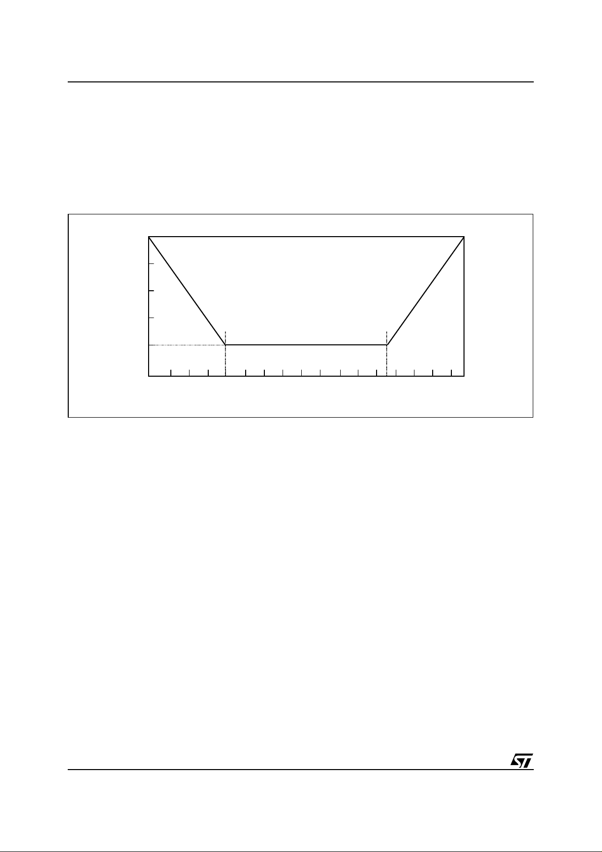
uPSD3234A, uPSD3234BV, uPSD3233B, uPSD3233BV
Receiver Characteristics
The uPSD323X Devices has a differential input receiver which is able to accept the USB data signal.
The receiver features an input sensitivity of at least
200mV when both differential data inputs are in
the range of at least 0.8V to 2 .5V with respect to
its local ground reference. This is the common
mode range, as shown in Figure 45. The receiver
Figure 45. Differential Input Sensitivity Over Entire Common Mode Range
1.0
0.8
0.6
0.4
0.2
Minimum Differential Sensitivity (volts)
0.0
0.0
0.2 0.4 0.6 0.8 1.0 1.2 1.4 1.6 1.8 2.0 2.2 2.4 2.6 2.8 3.0 3.2
Common Mode Input Voltage (volts)
tolerates static input voltages between -0.5V to
3.8V with respect to its local ground reference
without damage. In addition to the differential receiver, there is a single-ended receiver for each of
the two data lines. The single-ended receivers
have a switching threshold between 0.8V and 2.0V
(TTL inputs).
AI06630
90/170

uPSD3234A, uPSD3234BV, uPSD3233B, uPSD3233BV
External USB Pull-Up Resistor
The USB system specifies a pull-up resistor on the
D- pin for low-speed peripherals. The USB
Spec 1.1 describes a 1.5kΩ p ull-up resistor to a
3.3V supply. An approved alternative method is a
7.5kΩ pull-up to the USB V
supply. This alterna-
CC
Figure 46. USB Data Signal Timing and Voltage Levels
tive is defined for low-speed devices with an integrated cable. The chip is specified for the 7.5kΩ
pull-up. This eliminates the need for an external
3.3V regulator, or for a pin dedicated to provid ing
a 3.3V output from the chip.
t
V
OH
VCR
V
OL
D+
10%
D-
R
Figure 47. Receiver Jitter Tolerance
T
PERIOD
Differential
Data Lines
T
JR
Consecutive
Transitions
N*T
PERIOD+TJR1
90%
Paired
Transitions
N*T
PERIOD+TJR2
90%
t
F
10%
AI06631
T
JR1
T
JR2
AI06632
91/170

uPSD3234A, uPSD3234BV, uPSD3233B, uPSD3233BV
Figure 48. Differential to EOP Transition Skew and EOP Width
T
PERIOD
Differential
Data Lines
Crossover
Point
Crossover
Point Extended
Diff. Data to
SE0 Skew
N*T
PERIOD+TDEOP
Figure 49. Differential Data Jitter
T
PERIOD
Differential
Data Lines
Crossover
Points
Consecutive
Transitions
N*T
PERIOD+TxJR1
Paired
Transitions
N*T
PERIOD+TxJR2
Source EOP Width: T
Receiver EOP Width
T
, T
EOPR1
EOPR2
EOPT
AI06633
AI06634
92/170

uPSD3234A, uPSD3234BV, uPSD3233B, uPSD3233BV
Table 81. Transceiver DC Characteristics
Symb Parameter
V
OH
Static Output High
Test Conditions
15kΩ ± 5% to GND
(1)
(2,3)
Min Max Unit
2.8 3.6 V
V
OL
V
V
CM
V
SE
C
I
IO
R
PU
R
PD
Note: 1. VCC = 5V ± 10%; VSS = 0V; TA = 0 to 70°C.
2. Level guara nteed for ran ge of V
3. With RPU, external idle resistor, 7.5κ±2%, D- to V
Static Output Low Notes 2, 3 — 0.3 V
Differential Input Sensitivity
DI
|(D+) - (D-)|, Figure
47.,page91
0.2 — V
Differential Input Common Mode Figure 47., page 91 0.8 2.5 V
Single Ended Receiver Threshold — 0.8 2.0 V
Transceiver Capacitance — — 20 pF
IN
Data Line (D+, D-) Leakage 0V < (D+,D-) < 3.3 –10 10 µA
External Bus Pull-up Resistance, D-
7.5kΩ ± 2% to V
CC
7.35 7.65 kΩ
External Bus Pull-down Resistance 15kΩ ± 5% 14.25 15.75 kΩ
= 4.5V to 5.5V.
CC
CC
.
Table 82. Transceiver AC Characteristics
(5,6)
(5)
(5)
(1)
Min Max Unit
–75 75 ns
–45 45 ns
–40 100 ns
165 — ns
675 — ns
–95 95 ns
–150 150 ns
Symb Parameter
Test Conditions
tDRATE Low Speed Data Rate Ave. bit rate (1.5Mb/s ± 1.5%) 1.4775 1.5225 Mbit/s
tDJR1 Receiver Data Jitter Tolerance
tDJR2 Differential Input Sensitivity
tDEOP Differential to EOP Transition Skew
tEOPR1 EOP Width at Receiver
tEOPR2 EOP Width at Receiver
To next transition, Figure
47., page 91
(5)
For paired transition, Figure
47., page 91
(5)
Figure 48., page 92
Rejects as EOP
Accepts as EOP
tEOPT Source EOP Width — –1.25 1.50 µs
tUDJ1 Differential Driver Jitter
tUDJ2 Differential Driver Jitter
To next transition, Figure
49., page 92
To paired transition, Figure
49., page 92
tR USB Data Transition Rise Time Notes 2, 3, 4 75 300 ns
tF USB Data Transition Fall Time Notes 2, 3, 4 75 300 ns
tRFM Rise/Fall Time Matching
t
R
F
80 120 %
/ t
VCRS Output Signal Crossover Volt age — 1.3 2.0 V
Note: 1. VCC = 5V ± 10%; VSS = 0V; TA = 0 to 70°C.
2. Level guara nteed for ran ge of V
3. With RPU, external idle resistor, 7.5κ±2%, D- to V
4. C
of 50pF(75ns) to 350pF (300ns).
L
5. Measured at crossover point of differential da ta si gnals.
6. USB specifi c ation indicates 330ns.
= 4.5V to 5.5V.
CC
CC
.
93/170

uPSD3234A, uPSD3234BV, uPSD3233B, uPSD3233BV
PSD MODU LE
■ The PSD Module provides configurable
Program and Data memories to the 8032 CPU
core (MCU). In addition, it has its own set of I/
O ports and a PLD with 16 macrocells for
general logic implementation.
■ Ports A,B,C, and D are general purpose
programmable I/O ports that have a port
architecture which is different from the I/O
ports in the MCU Module.
■ The PSD Module communicates with the MCU
Module through the internal address, data bus
(A0-A15, D0-D7) and control signals (RD
, ALE, RESET). The user defines the
PSEN
, WR,
Decoding PLD in the PSDsoft Development
Tool and can map the resources in the PSD
Module to any program or data address
space. Figure 50., page 95 shows the
functional blocks in the PSD Module.
Functional Overview
– 1 or 2 Mbit Flash memory. This is the main
Flash memory. It is divided into eight equalsized blocks that can be accessed with userspecified addresses.
– Secondary 256 Kbit Flash boot memory. It is
divided into four equal-sized blocks that can
be accessed with user-specified addresses.
This secondary memory brings the ability to
execute code and update the main Flash
concurrently.
– 64 Kbit SRAM. The SRAM’s contents can be
protected from a power failure by connecting
an external batter y.
– CPLD with 16 Output Micro Cells (OMCs} and
20 Input Micro Cells (IMCs). The CPLD may
be used to efficiently implement a variety of
logic functions for internal and external
control. Examples include state machines,
loadable shift registers, and loadable
counters.
– Decode PLD (DPLD) that decodes address for
selection of memory blocks in the PSD
Module.
– Configurable I/O ports (Port A,B,C and D) that
can be used for the following functions:
MCU I/Os
PLD I/Os
Latched MCU address output
Special function I/Os.
I/O ports may be configured as open-drain
outputs.
– Built-in JTAG compliant serial port allows full-
chip In-S ystem P ro grammabi lity ( ISP) . W ith i t ,
you can program a blank device or reprogram
a device in the factory or the field.
– Internal page register that can be used to
expand the 8032 MCU Module address space
by a factor of 256.
– Internal programmable Power Managem ent
Unit (PMU) that supports a low-power mode
called Power-down Mode. The PMU can
automatically detect a lack of the 8032 CPU
core activity and put the PSD Module into
Power-down Mode.
– Erase/WRITE cycles:
Flash memory - 100,000 minimum
PLD - 1,000 minimum
Data Retention: 15 year minimum (for Main
Flash memory, Boot, PLD and Configuration
bits)
94/170

Figure 50. PSD Module Block Diagram
)
PC2
(
VSTDBY
uPSD3234A, uPSD3234BV, uPSD3233B, uPSD3233BV
PA0 – PA7
PB0 – PB7
PC0 – PC7
PD1 – PD2
ADDRESS/DATA/CONTROL BUS
UNIT
POWER
MANGMT
8 SECTORS
FLASH MEMORY
1 OR 2 MBIT PRIMARY
EMBEDDED
PAGE
REGISTER
256 KBIT SECONDARY
SECTOR
ALGORITHM
8
PORT
PROG.
4 SECTORS
(BOOT OR DATA)
NON-VOLATILE MEMORY
SELECTS
)
DPLD
(
PLD
FLASH DECODE
SECTOR
SELECTS
73
BACKUP SRAM
64 KBIT BATTERY
SRAM SELECT
A
PORT
RUNTIME CONTROL
AND I/O REGISTERS
PERIP I/O MODE SELECTS
CSIOP
PORT
PROG.
2 EXT CS TO PORT D
16 OUTPUT MACROCELLS
(CPLD)
FLASH ISP CPLD
73
B
PORT
PORT A ,B & C
PORT A ,B & C
20 INPUT MACROCELLS
CLKIN
C
PORT
PORT
PROG.
MACROCELL FEEDBACK OR PORT INPUT
CLKIN
PORT
PORT
PROG.
JTAG
SERIAL
& FLASH MEMORY
PLD, CONFIGURATION
D
CHANNEL
LOADER
8032 Bus
PLD
BUS
INPUT
WR_, RD_,
PSEN_, ALE,
RESET_,
BUS
Interface
A0-A15
BUS
Interface
D0 – D7
GLOBAL
SECURITY
CONFIG. &
CLKIN
(PD1)
AI05797
95/170

uPSD3234A, uPSD3234BV, uPSD3233B, uPSD3233BV
In-Syst em Prog r a mming ( ISP)
Using the JTAG signals on Port C, the entire PSD
Module device can be programmed or erased
without the use of the MCU. The primary Flash
memory can also be programmed in-system by
the MCU executing the programming algorithms
out of the secondary memory, or SRAM. The secondary memory can be programmed the same
Tabl e 83. Methods of Progra m m i ng Different Functional B l ocks of t he PSD Module
Functional Block JTAG Programming Device Programmer IAP
Primary Flash Memory Yes Yes Yes
Secondary Flash Memory Yes Yes Yes
PLD Array (DPLD and CPLD) Yes Yes No
PSD Module Configuration Yes Yes No
way by executing out of the pri mary F lash m em ory. The PLD or other PSD Module Configuration
blocks can be pr ogrammed thro ugh the JTAG port
or a device programmer. Table 83 in d i ca te s which
programming methods can program different functional blocks of the PSD Module .
96/170

uPSD3234A, uPSD3234BV, uPSD3233B, uPSD3233BV
DEVELOP MEN T SYSTEM
The uPSD3200 is supported by PSDsof t, a Windows-based software development tool (Windows-95, Windows-98, Windows-NT). A PSD
Module design is quickly and easily produced in a
point and click environment. The designer does
not need to enter Hardware Description Language
(HDL) equations, unless desired, to define PSD
Module pin functions and mem ory map information. The general design flow is shown in Figure
51. PSDsoft is available from our web site (the ad-
Figure 51. PSDsoft Express Development Tool
Choose µPSD
Define µPSD Pin and
Node Functions
Point and click definition of
PSD pin functions, internal nodes,
and MCU system memory map
dress is given on the back page of this data sheet)
or other distribution channels.
PSDsoft directly supports a low cost device programmer from ST: FlashLINK (JTAG). The programmer may be purchased through your local
distributor/representative. The uPS D3200 is also
supported by third party device programmers. See
our web site for the current list.
Define General Purpose
Logic in CPLD
Point and click definition of combinatorial and registered logic in CPLD.
Access HDL is available if needed
Merge MCU Firmware with
PSD Module Configuration
A composite object file is created
containing MCU firmware and
PSD configuration
*.OBJ FILE
PSD Programmer
FlashLINK (JTAG)
MCU FIRMWARE
HEX OR S-RECORD
FORMAT
*.OBJ FILE
AVAILABLE
FOR 3rd PARTY
PROGRAMMERS
C Code Generation
GENERATE C CODE
SPECIFIC TO PSD
FUNCTIONS
USER'S CHOICE OF
8032
COMPILER/LINKER
AI05798
97/170

uPSD3234A, uPSD3234BV, uPSD3233B, uPSD3233BV
PSD MODU LE REGISTER DESCRIPTION AND ADDRESS OFFSET
Table 84 shows the offset addresses to the PSD
Module registers relative to the CSIOP base address. The CSIOP space is the 256 bytes of address that is allocated by the user to the inte rnal
Table 84. Register Address Offset
Register Name Port A Port B Port C Port D
Data In 00 01 10 11 Reads Port pin as input, MCU I/O Input Mode
Control 02 03 Selects mode between MCU I/O or Address Out
PSD Module registers. Table 84 provides brief descriptions of the registers in CSIOP space. The following section gives a more detailed description.
Other
(1)
Description
Data Out 04 05 12 13
Direction 06 07 14 15 Configures Port pin as input or output
Drive Select 08 09 16 17
Input Macrocell 0A 0B 18 Reads Input Macrocells
Enable Out 0C 0D 1A 1B
Output Macrocells
AB
Output Macrocells
BC
Mask Macrocells AB 22 22 Blocks writing to the Output Macrocells AB
Mask Macrocells BC 23 23 Blocks writing to the Output Macrocells BC
Primary Flash
Protection
Secondary Flash
memory Protection
PMMR0 B0 Power Management Register 0
PMMR2 B4 Power Management Register 2
Page E0 Page Register
VM E2
Note: 1. Other registers that are not part of th e I/O ports.
20 20
21 21
C0 Read-only – Primary Flash Sector Protection
C2
Stores data for output to Port pins, MCU I/O
Output Mode
Configures Port pins as either CMOS or Open
Drain on some pins, while selecting high slew rate
on other pins.
Reads the status of the output enable to the I/O
Port driver
READ – reads output of macrocells AB
WRITE – loads macrocell flip-flops
READ – reads output of macrocells BC
WRITE – loads macrocell flip-flops
Read-only – PSD Module Security and Secondary
Flash memory Sector Protection
Places PSD Module memory areas in Program
and/or Data space on an individual basis.
98/170

uPSD3234A, uPSD3234BV, uPSD3233B, uPSD3233BV
PSD MODU LE DETAILED OPER ATION
As shown in Figure 15., page 27, the PSD Module
consists of five major types of functional blocks:
■ Memory Block
■ PLD Blocks
■ I/O Ports
■ Power Management Unit (PMU)
■ JTAG Interface
The functions of ea ch block are described in t he
following sections. Many of the blocks perform
multiple functions, and are user configurable.
MEMORY BLOCKS
The PSD Module has the following memory
blocks:
■ Primary Flash memory
■ Secondary Flash memory
■ SRAM
The Memory Select signals for these blocks originate from the Decode PLD (DPLD) an d are userdefined in PSDsoft Express.
Primary Flash Memory and Secon dary F lash memory Description
The primary Flash memory is divided evenly into
eight equal sectors. The secondary Flash memory
is divided into four e qual sectors. Each sector of
either memory block can be sepa rately protected
from Program and Erase cycles.
Flash memory may be erased on a sector-by-sector basis. Flash sector erasure may be suspended
while data is read from other sectors of the block
and then resumed after reading.
During a Program or Erase cycle in Flash memory,
the status can be output on Ready/Busy
This pin is set up using PSDsoft Express Configuration.
(PC3).
Memory Block Select Signals
The DPLD generates the Select signals for all the
internal memory blocks (see PLDs, page 112).
Each of the eight sectors of the primary Flash
memory has a Select signal (FS0-FS7) which can
contain up to three product terms. Each of the four
sectors of the secondary Flash memory has a Select signal (CSBOOT0-CSBOOT3) which can contain up to three product terms. Having three
product terms for each Select signal allows a given
sector to be mapped in Program or Data space.
Ready/Busy
output the Ready/Busy
ry. The output on Ready/Busy
when Flash memory is being written to,
(PC3 ). This signal can be used to
status of the Flash memo-
(PC3) is a '0' (Busy)
or
when
Flash memory is being erased. The output is a '1'
(Ready) when no WRITE or Erase cycle is in
progress.
Memory Operation. The primary Flash memory
and secondary Flash memory are addressed
through the MCU Bus. The MCU can access these
memories in one of two ways:
– The MCU can execute a typical bus WRITE or
READ
operation
.
– The MCU can execute a specific Flash
memory in s truction that consists of several
WRITE and READ operations. This involves
writing specific data patterns to special
addresses within the Flash memory to invoke
an embedded algorithm. These instructions
are summarized in T able 85., page 101.
Typically, the MCU can read Flash memory using
READ operations, just as it would read a ROM device. However, Flash memory can only be altered
using specific Erase and Program instructions. For
example, the MCU cannot write a single byte directly to Flash memory as it would write a byte to
RAM. To program a byte into F lash memory, the
MCU must execute a Program instruction, then
test the status of the Program cycle. This status
test is achieved by a RE AD operation or polling
Ready/Busy
(PC3).
99/170

uPSD3234A, uPSD3234BV, uPSD3233B, uPSD3233BV
Instructions
An instruction consists of a sequence o f specific
operations. Each received byte is sequentially decoded by the PSD Module and not executed as a
standard WRITE operation. The instruction is executed when the correct number of bytes are properly received and the time between two
consecutive bytes is shorter t han the t ime-out period. Some instructions are structured to in clude
READ operations after the initial WRITE operations.
The instruction must be followed exactly. Any invalid combination of instruction bytes or time-out
between two consecutive byte s while addressing
Flash memory resets the device logic into READ
Mode (Flash memory is read like a ROM device).
The Flash memory supports the instructions summarized in Table 85:
Flash memory:
– Erase memory by chip or sector
– Suspend or resume sector erase
– Program a Byte
– RESET to READ Mode
– Read Sector Protection Status
– Bypass
These instructions are detailed in Table 85. For ef-
ficient decoding of the instructions, the first two
bytes of an instruction are the coded c ycles and
are followed by an instruction byte or confirmation
byte. The coded cycles consist of writing the data
AAh to address X555h during the first cycle and
data 55h to address XAAAh duri ng the second cycle. Address signals A15-A12 are Don’t Care during the instruction WRITE cycles. However, the
appropriate Sector Select (FS0-FS7 or
CSBOOT0-CSBOOT3) must be selected.
The primary and secondary Flash memories have
the same instruction set (except for Read Primary
Flash Identifier). The Sector Select signals determine which Flash memory is to receive and execute the instruction. The primary Flash memory is
selected if any one of Sector Select (FS0-FS7) is
High, and the secondary Flash memory is selected
if any one of Sector Select (CSBOOT0CSBOOT3) is High.
100/170
 Loading...