


Flash Program mable System Devices
with 8032 Microcontroller Core and 64 Kbit SRAM
FEAT URES SUM MARY
■ FAST 8-BIT 8032 MCU
– 40MHz at 5.0V, 24MHz at 3.3V
– Core, 12-clocks per instruction
■ DUAL FLASH MEMORIES WITH MEMORY
MANAGEMENT
– Place either memory into 8032 program
address space or data address space
– READ-while-WRITE operation for In-
Application Programming and EEPR OM
emulation
– Single voltage program and erase
– 100K minimum erase cycl e s, 1 5 -ye a r
retention
■ CLOCK, RESET, AND SUPPLY
MANAGEMENT
– SRAM is Battery Backup capable
– Normal, Idle, and Power Down Modes
– Power-on and Low Voltage reset
supervisor
– Programmable Watchdog Timer
■ PROGRAMMABLE LOGIC, GENERAL
PURPOSE
– 16 macrocells
– Implements state machines, glue-logic,
and so forth
■ COMMUNICATION INTERFACES
– USB v1.1, low-speed 1.5Mbps, 3
endpoints
2
C Master/Slave bus controller
–I
– Two UARTs with independent baud rate
– Six I/O ports with up to 46 I/O pins
– 8032 Address/Data bus available on
TQFP80 packa ge
– 5 PWM outputs, 8-bit resolution
■ JTAG IN-SYSTEM PROG RAMMING
– Program the entire device in as little as
10 seconds
uPSD3234A, uPSD3234BV
uPSD3233B, uPSD3233BV
Figure 1. Packages
TQFP52 (T)
52-lead, Thin,
Quad Flat
TQFP80 (U)
80-lead, Thin,
Qual Flat
■ A/D CONVERTER
– Four channels, 8-bit resolution, 10µs
■ TIMERS AND INTERRUPTS
– Three 8032 standard 16-bit timers
– 10 Interrupt sources with two external
interrupt pins
■ Single Supply Voltage
– 4.5 to 5.5V
– 3.0 to 3.6V
1/170November 2004

uPSD3234A, uPSD3234BV, uPSD3233B, uPSD3233BV
Table 1. Device Summary
Max
Part Number
uPSD3233B-40T6 40 128K 32K 8K 37 No No 4.5-5.5 TQFP52 –40°C to 85°C
uPSD3233BV-24T6 24 128K 32K 8K 37 No No 3.0-3.6 TQFP52 –40°C to 85°C
uPSD3233B-40U6 40 128K 32K 8K 46 No Yes 4.5-5.5 TQFP80 –40°C to 85°C
uPSD3233BV-24U6 24 128K 32K 8K 46 No Yes 3.0-3.6 TQFP80 –40°C to 85°C
uPSD3234A-40T6 40 256K 32K 8K 37 Yes No 4.5-5.5 TQFP52 –40°C to 85°C
uPSD3234A-40U6 40 256K 32K 8K 46 Yes Yes 4.5-5.5 TQFP80 –40°C to 85°C
uPSD3234BV-24U6 24 256K 32K 8K 46 No Yes 3.0-3.6 TQFP80 –40°C to 85°C
Clock
(MHz)
1st
Flash
(bytes)
2nd
Flash
(bytes)
SRAM
(bytes)
GPIO USB
8032
Bus
V
(V)
CC
Pkg. Temp.
2/170

uPSD3234A, uPSD3234BV, uPSD3233B, uPSD3233BV
TABLE OF CONTENTS
FEATURES SUMMARY . . . . . . . . . . . . . . . . . . . . . . . . . . . . . . . . . . . . . . . . . . . . . . . . . . . . . . . . . . . . . 1
SUMMARY DESCRIPTION. . . . . . . . . . . . . . . . . . . . . . . . . . . . . . . . . . . . . . . . . . . . . . . . . . . . . . . . . . . 7
52-PIN PACKAGE I/O PORT . . . . . . . . . . . . . . . . . . . . . . . . . . . . . . . . . . . . . . . . . . . . . . . . . . . . . . . . 12
ARCHITECTURE OVERVIEW . . . . . . . . . . . . . . . . . . . . . . . . . . . . . . . . . . . . . . . . . . . . . . . . . . . . . . . 13
Memory Organization . . . . . . . . . . . . . . . . . . . . . . . . . . . . . . . . . . . . . . . . . . . . . . . . . . . . . . . . . . 13
Registers . . . . . . . . . . . . . . . . . . . . . . . . . . . . . . . . . . . . . . . . . . . . . . . . . . . . . . . . . . . . . . . . . . . . 13
Program Memory. . . . . . . . . . . . . . . . . . . . . . . . . . . . . . . . . . . . . . . . . . . . . . . . . . . . . . . . . . . . . . 15
Data memory . . . . . . . . . . . . . . . . . . . . . . . . . . . . . . . . . . . . . . . . . . . . . . . . . . . . . . . . . . . . . . . . . 15
RAM . . . . . . . . . . . . . . . . . . . . . . . . . . . . . . . . . . . . . . . . . . . . . . . . . . . . . . . . . . . . . . . . . . . . . . . . 15
XRAM-DDC. . . . . . . . . . . . . . . . . . . . . . . . . . . . . . . . . . . . . . . . . . . . . . . . . . . . . . . . . . . . . . . . . . . 15
XRAM-PSD . . . . . . . . . . . . . . . . . . . . . . . . . . . . . . . . . . . . . . . . . . . . . . . . . . . . . . . . . . . . . . . . . . . 15
SFR . . . . . . . . . . . . . . . . . . . . . . . . . . . . . . . . . . . . . . . . . . . . . . . . . . . . . . . . . . . . . . . . . . . . . . . . . 16
Addressing Modes . . . . . . . . . . . . . . . . . . . . . . . . . . . . . . . . . . . . . . . . . . . . . . . . . . . . . . . . . . . . 16
Arithmetic Instructions. . . . . . . . . . . . . . . . . . . . . . . . . . . . . . . . . . . . . . . . . . . . . . . . . . . . . . . . . 17
Logical Instructions . . . . . . . . . . . . . . . . . . . . . . . . . . . . . . . . . . . . . . . . . . . . . . . . . . . . . . . . . . . 18
Data Transfers . . . . . . . . . . . . . . . . . . . . . . . . . . . . . . . . . . . . . . . . . . . . . . . . . . . . . . . . . . . . . . . . 20
Boolean Instructions. . . . . . . . . . . . . . . . . . . . . . . . . . . . . . . . . . . . . . . . . . . . . . . . . . . . . . . . . . . 23
Relative Offset . . . . . . . . . . . . . . . . . . . . . . . . . . . . . . . . . . . . . . . . . . . . . . . . . . . . . . . . . . . . . . . . 23
Jump Instructions . . . . . . . . . . . . . . . . . . . . . . . . . . . . . . . . . . . . . . . . . . . . . . . . . . . . . . . . . . . . . 24
Machine Cycles . . . . . . . . . . . . . . . . . . . . . . . . . . . . . . . . . . . . . . . . . . . . . . . . . . . . . . . . . . . . . . . 25
uPSD3200 HARDWARE DESCRIPTION . . . . . . . . . . . . . . . . . . . . . . . . . . . . . . . . . . . . . . . . . . . . . . . 27
MCU MODULE DISCRIPTION . . . . . . . . . . . . . . . . . . . . . . . . . . . . . . . . . . . . . . . . . . . . . . . . . . . . . . . 28
Special Function Registers . . . . . . . . . . . . . . . . . . . . . . . . . . . . . . . . . . . . . . . . . . . . . . . . . . . . . 28
INTERRUPT SYSTEM. . . . . . . . . . . . . . . . . . . . . . . . . . . . . . . . . . . . . . . . . . . . . . . . . . . . . . . . . . . . . . 35
External Int0. . . . . . . . . . . . . . . . . . . . . . . . . . . . . . . . . . . . . . . . . . . . . . . . . . . . . . . . . . . . . . . . . . 35
Timer 0 and 1 Interrupts . . . . . . . . . . . . . . . . . . . . . . . . . . . . . . . . . . . . . . . . . . . . . . . . . . . . . . . . 35
Timer 2 Interrupt . . . . . . . . . . . . . . . . . . . . . . . . . . . . . . . . . . . . . . . . . . . . . . . . . . . . . . . . . . . . . . 35
2
I
C Interrupt . . . . . . . . . . . . . . . . . . . . . . . . . . . . . . . . . . . . . . . . . . . . . . . . . . . . . . . . . . . . . . . . . . 35
External Int1. . . . . . . . . . . . . . . . . . . . . . . . . . . . . . . . . . . . . . . . . . . . . . . . . . . . . . . . . . . . . . . . . . 35
DDC Interrupt . . . . . . . . . . . . . . . . . . . . . . . . . . . . . . . . . . . . . . . . . . . . . . . . . . . . . . . . . . . . . . . . . 35
USB Interrupt. . . . . . . . . . . . . . . . . . . . . . . . . . . . . . . . . . . . . . . . . . . . . . . . . . . . . . . . . . . . . . . . . 35
USART Interrupt . . . . . . . . . . . . . . . . . . . . . . . . . . . . . . . . . . . . . . . . . . . . . . . . . . . . . . . . . . . . . . 36
Interrupt Priority Structure. . . . . . . . . . . . . . . . . . . . . . . . . . . . . . . . . . . . . . . . . . . . . . . . . . . . . . 3 7
Interrupts Enable Structure . . . . . . . . . . . . . . . . . . . . . . . . . . . . . . . . . . . . . . . . . . . . . . . . . . . . . 37
How Interrupts are Handled . . . . . . . . . . . . . . . . . . . . . . . . . . . . . . . . . . . . . . . . . . . . . . . . . . . . . 39
POWER-SAVING MODE. . . . . . . . . . . . . . . . . . . . . . . . . . . . . . . . . . . . . . . . . . . . . . . . . . . . . . . . . . . . 40
Idle Mode . . . . . . . . . . . . . . . . . . . . . . . . . . . . . . . . . . . . . . . . . . . . . . . . . . . . . . . . . . . . . . . . . . . . 40
3/170

uPSD3234A, uPSD3234BV, uPSD3233B, uPSD3233BV
Power-Down Mode . . . . . . . . . . . . . . . . . . . . . . . . . . . . . . . . . . . . . . . . . . . . . . . . . . . . . . . . . . . . 40
Power Control Register. . . . . . . . . . . . . . . . . . . . . . . . . . . . . . . . . . . . . . . . . . . . . . . . . . . . . . . . . 4 0
Idle Mode . . . . . . . . . . . . . . . . . . . . . . . . . . . . . . . . . . . . . . . . . . . . . . . . . . . . . . . . . . . . . . . . . . . . 41
Power-Down Mode . . . . . . . . . . . . . . . . . . . . . . . . . . . . . . . . . . . . . . . . . . . . . . . . . . . . . . . . . . . . 41
I/O PORTS (MCU MODULE). . . . . . . . . . . . . . . . . . . . . . . . . . . . . . . . . . . . . . . . . . . . . . . . . . . . . . . . . 42
PORT Type and Description . . . . . . . . . . . . . . . . . . . . . . . . . . . . . . . . . . . . . . . . . . . . . . . . . . . . . 43
OSCILLATOR . . . . . . . . . . . . . . . . . . . . . . . . . . . . . . . . . . . . . . . . . . . . . . . . . . . . . . . . . . . . . . . . . . . . 45
SUPERVISORY. . . . . . . . . . . . . . . . . . . . . . . . . . . . . . . . . . . . . . . . . . . . . . . . . . . . . . . . . . . . . . . . . . . 45
External Reset . . . . . . . . . . . . . . . . . . . . . . . . . . . . . . . . . . . . . . . . . . . . . . . . . . . . . . . . . . . . . . . . 46
Low VDD Voltage Reset . . . . . . . . . . . . . . . . . . . . . . . . . . . . . . . . . . . . . . . . . . . . . . . . . . . . . . . . 4 6
Watchdog Timer Overflow . . . . . . . . . . . . . . . . . . . . . . . . . . . . . . . . . . . . . . . . . . . . . . . . . . . . . . 46
USB Reset . . . . . . . . . . . . . . . . . . . . . . . . . . . . . . . . . . . . . . . . . . . . . . . . . . . . . . . . . . . . . . . . . . . 46
WATCHDOG TIMER. . . . . . . . . . . . . . . . . . . . . . . . . . . . . . . . . . . . . . . . . . . . . . . . . . . . . . . . . . . . . . . 47
TIMER/COUNTERS (TIMER 0, TIMER 1 AND TIMER 2). . . . . . . . . . . . . . . . . . . . . . . . . . . . . . . . . . . 49
Timer 0 and Timer 1. . . . . . . . . . . . . . . . . . . . . . . . . . . . . . . . . . . . . . . . . . . . . . . . . . . . . . . . . . . . 49
Timer 2 . . . . . . . . . . . . . . . . . . . . . . . . . . . . . . . . . . . . . . . . . . . . . . . . . . . . . . . . . . . . . . . . . . . . . . 53
STANDARD SERIAL INTERFACE (UART) . . . . . . . . . . . . . . . . . . . . . . . . . . . . . . . . . . . . . . . . . . . . . 56
Multiprocessor Comm u ni cations. . . . . . . . . . . . . . . . . . . . . . . . . . . . . . . . . . . . . . . . . . . . . . . . . 56
Serial Port Control Register . . . . . . . . . . . . . . . . . . . . . . . . . . . . . . . . . . . . . . . . . . . . . . . . . . . . . 56
ANALOG-TO-DIGITAL CONVERTOR (ADC) . . . . . . . . . . . . . . . . . . . . . . . . . . . . . . . . . . . . . . . . . . . 65
ADC Interrupt . . . . . . . . . . . . . . . . . . . . . . . . . . . . . . . . . . . . . . . . . . . . . . . . . . . . . . . . . . . . . . . . . 65
PULSE WIDTH MODULATION (PWM). . . . . . . . . . . . . . . . . . . . . . . . . . . . . . . . . . . . . . . . . . . . . . . . . 67
4-channel PWM Unit (PWM 0-3) . . . . . . . . . . . . . . . . . . . . . . . . . . . . . . . . . . . . . . . . . . . . . . . . . .67
Programmable Period 8-bit PWM. . . . . . . . . . . . . . . . . . . . . . . . . . . . . . . . . . . . . . . . . . . . . . . . . 69
PWM 4 Channel Operation . . . . . . . . . . . . . . . . . . . . . . . . . . . . . . . . . . . . . . . . . . . . . . . . . . . . . . 7 0
2
I
C INTERFACE . . . . . . . . . . . . . . . . . . . . . . . . . . . . . . . . . . . . . . . . . . . . . . . . . . . . . . . . . . . . . . . . . . 71
Serial Status Register (SxSTA: S1STA, S2STA). . . . . . . . . . . . . . . . . . . . . . . . . . . . . . . . . . . . . 73
Data Shift Register (SxDAT: S1DAT, S2DAT) . . . . . . . . . . . . . . . . . . . . . . . . . . . . . . . . . . . . . . . 73
Address Register (SxADR: S1ADR, S2ADR). . . . . . . . . . . . . . . . . . . . . . . . . . . . . . . . . . . . . . . . 74
DDC INTERFACE . . . . . . . . . . . . . . . . . . . . . . . . . . . . . . . . . . . . . . . . . . . . . . . . . . . . . . . . . . . . . . . . . 75
Special Function Register for the DDC Interface . . . . . . . . . . . . . . . . . . . . . . . . . . . . . . . . . . . . 76
Host Type Detection . . . . . . . . . . . . . . . . . . . . . . . . . . . . . . . . . . . . . . . . . . . . . . . . . . . . . . . . . . . 79
DDC1 Protocol. . . . . . . . . . . . . . . . . . . . . . . . . . . . . . . . . . . . . . . . . . . . . . . . . . . . . . . . . . . . . . . . 80
DDC2B Protocol. . . . . . . . . . . . . . . . . . . . . . . . . . . . . . . . . . . . . . . . . . . . . . . . . . . . . . . . . . . . . . . 81
USB HARDWARE. . . . . . . . . . . . . . . . . . . . . . . . . . . . . . . . . . . . . . . . . . . . . . . . . . . . . . . . . . . . . . . . . 82
4/170

uPSD3234A, uPSD3234BV, uPSD3233B, uPSD3233BV
USB related registers . . . . . . . . . . . . . . . . . . . . . . . . . . . . . . . . . . . . . . . . . . . . . . . . . . . . . . . . . . 82
Transceiver . . . . . . . . . . . . . . . . . . . . . . . . . . . . . . . . . . . . . . . . . . . . . . . . . . . . . . . . . . . . . . . . . . 89
Receiver Characteristics. . . . . . . . . . . . . . . . . . . . . . . . . . . . . . . . . . . . . . . . . . . . . . . . . . . . . . . . 90
External USB Pull-Up Resistor. . . . . . . . . . . . . . . . . . . . . . . . . . . . . . . . . . . . . . . . . . . . . . . . . . . 91
PSD MODULE. . . . . . . . . . . . . . . . . . . . . . . . . . . . . . . . . . . . . . . . . . . . . . . . . . . . . . . . . . . . . . . . . . . . 94
Functional Overview . . . . . . . . . . . . . . . . . . . . . . . . . . . . . . . . . . . . . . . . . . . . . . . . . . . . . . . . . . . 94
In-System Programming (ISP) . . . . . . . . . . . . . . . . . . . . . . . . . . . . . . . . . . . . . . . . . . . . . . . . . . .96
DEVELOPMENT SYSTEM . . . . . . . . . . . . . . . . . . . . . . . . . . . . . . . . . . . . . . . . . . . . . . . . . . . . . . . . . . 97
PSD MODULE REGISTER DESCRIPTION AND ADDRESS OFFSET . . . . . . . . . . . . . . . . . . . . . . . . 98
PSD MODULE DETAILED OPERATION . . . . . . . . . . . . . . . . . . . . . . . . . . . . . . . . . . . . . . . . . . . . . . . 99
MEMORY BLOCKS. . . . . . . . . . . . . . . . . . . . . . . . . . . . . . . . . . . . . . . . . . . . . . . . . . . . . . . . . . . . . . . . 99
Primary Flash Memo ry and Seco nd ary Flash memo ry Description. . . . . . . . . . . . . . . . . . . . . 99
Memory Block Select Signals. . . . . . . . . . . . . . . . . . . . . . . . . . . . . . . . . . . . . . . . . . . . . . . . . . . . 99
Instructions . . . . . . . . . . . . . . . . . . . . . . . . . . . . . . . . . . . . . . . . . . . . . . . . . . . . . . . . . . . . . . . . . 100
Power-down Instruction and Power-up Mode . . . . . . . . . . . . . . . . . . . . . . . . . . . . . . . . . . . . . 102
READ . . . . . . . . . . . . . . . . . . . . . . . . . . . . . . . . . . . . . . . . . . . . . . . . . . . . . . . . . . . . . . . . . . . . . .102
Programming Flash Memory . . . . . . . . . . . . . . . . . . . . . . . . . . . . . . . . . . . . . . . . . . . . . . . . . . . 104
Erasing Flash Memory . . . . . . . . . . . . . . . . . . . . . . . . . . . . . . . . . . . . . . . . . . . . . . . . . . . . . . . . 106
Specific Features. . . . . . . . . . . . . . . . . . . . . . . . . . . . . . . . . . . . . . . . . . . . . . . . . . . . . . . . . . . . .107
SRAM . . . . . . . . . . . . . . . . . . . . . . . . . . . . . . . . . . . . . . . . . . . . . . . . . . . . . . . . . . . . . . . . . . . . . . 108
Sector Select and SRAM Select. . . . . . . . . . . . . . . . . . . . . . . . . . . . . . . . . . . . . . . . . . . . . . . . .108
Page Register. . . . . . . . . . . . . . . . . . . . . . . . . . . . . . . . . . . . . . . . . . . . . . . . . . . . . . . . . . . . . . . . 111
PLDs . . . . . . . . . . . . . . . . . . . . . . . . . . . . . . . . . . . . . . . . . . . . . . . . . . . . . . . . . . . . . . . . . . . . . . . . . . 112
The Turbo Bit in PSD Module. . . . . . . . . . . . . . . . . . . . . . . . . . . . . . . . . . . . . . . . . . . . . . . . . . . 112
Decode PLD (DPLD) . . . . . . . . . . . . . . . . . . . . . . . . . . . . . . . . . . . . . . . . . . . . . . . . . . . . . . . . . . 11 4
Complex PLD (CPLD) . . . . . . . . . . . . . . . . . . . . . . . . . . . . . . . . . . . . . . . . . . . . . . . . . . . . . . . . . 115
Output Macrocell (OMC) . . . . . . . . . . . . . . . . . . . . . . . . . . . . . . . . . . . . . . . . . . . . . . . . . . . . . . . 116
Product Term Allocator. . . . . . . . . . . . . . . . . . . . . . . . . . . . . . . . . . . . . . . . . . . . . . . . . . . . . . . . 117
Input Macrocells (IMC) . . . . . . . . . . . . . . . . . . . . . . . . . . . . . . . . . . . . . . . . . . . . . . . . . . . . . . . . 118
I/O PORTS (PSD MODULE) . . . . . . . . . . . . . . . . . . . . . . . . . . . . . . . . . . . . . . . . . . . . . . . . . . . . . . . . 119
General Port Architecture . . . . . . . . . . . . . . . . . . . . . . . . . . . . . . . . . . . . . . . . . . . . . . . . . . . . . . 119
Port Operating Modes. . . . . . . . . . . . . . . . . . . . . . . . . . . . . . . . . . . . . . . . . . . . . . . . . . . . . . . . . 120
MCU I/O Mode . . . . . . . . . . . . . . . . . . . . . . . . . . . . . . . . . . . . . . . . . . . . . . . . . . . . . . . . . . . . . . . 120
PLD I/O Mode. . . . . . . . . . . . . . . . . . . . . . . . . . . . . . . . . . . . . . . . . . . . . . . . . . . . . . . . . . . . . . . . 120
Address Out Mod e . . . . . . . . . . . . . . . . . . . . . . . . . . . . . . . . . . . . . . . . . . . . . . . . . . . . . . . . . . . . 120
Peripheral I/O Mode. . . . . . . . . . . . . . . . . . . . . . . . . . . . . . . . . . . . . . . . . . . . . . . . . . . . . . . . . . . 120
JTAG In-System Programming (ISP). . . . . . . . . . . . . . . . . . . . . . . . . . . . . . . . . . . . . . . . . . . . . 120
Port Configuration Registers (PCR) . . . . . . . . . . . . . . . . . . . . . . . . . . . . . . . . . . . . . . . . . . . . . 122
Port Data Registers. . . . . . . . . . . . . . . . . . . . . . . . . . . . . . . . . . . . . . . . . . . . . . . . . . . . . . . . . . . 123
5/170

uPSD3234A, uPSD3234BV, uPSD3233B, uPSD3233BV
Ports A and B – Functionality and Structure . . . . . . . . . . . . . . . . . . . . . . . . . . . . . . . . . . . . . . 124
Port C – Functionality and Structure. . . . . . . . . . . . . . . . . . . . . . . . . . . . . . . . . . . . . . . . . . . . . 125
Port D – Functionality and Structure. . . . . . . . . . . . . . . . . . . . . . . . . . . . . . . . . . . . . . . . . . . . . 126
External Chip Select . . . . . . . . . . . . . . . . . . . . . . . . . . . . . . . . . . . . . . . . . . . . . . . . . . . . . . . . . . 127
POWER MANAGEMENT . . . . . . . . . . . . . . . . . . . . . . . . . . . . . . . . . . . . . . . . . . . . . . . . . . . . . . . . . . 1 2 8
PLD Power Management. . . . . . . . . . . . . . . . . . . . . . . . . . . . . . . . . . . . . . . . . . . . . . . . . . . . . . . 130
PSD Chip Select Input (CSI, PD2) . . . . . . . . . . . . . . . . . . . . . . . . . . . . . . . . . . . . . . . . . . . . . . . 130
Input Clock . . . . . . . . . . . . . . . . . . . . . . . . . . . . . . . . . . . . . . . . . . . . . . . . . . . . . . . . . . . . . . . . . . 130
Input Control Signals . . . . . . . . . . . . . . . . . . . . . . . . . . . . . . . . . . . . . . . . . . . . . . . . . . . . . . . . . 130
RESET TIMING AND DEVICE STATUS AT RESET . . . . . . . . . . . . . . . . . . . . . . . . . . . . . . . . . . . . . 132
Warm RESET . . . . . . . . . . . . . . . . . . . . . . . . . . . . . . . . . . . . . . . . . . . . . . . . . . . . . . . . . . . . . . . . 132
I/O Pin, Register and PLD Status at RESET . . . . . . . . . . . . . . . . . . . . . . . . . . . . . . . . . . . . . . . 132
Reset of Flash Memory Erase and Program Cycle s . . . . . . . . . . . . . . . . . . . . . . . . . . . . . . . . . 132
PROGRAMMING IN-CIRCUIT USING THE JTAG SERIAL INTERFACE . . . . . . . . . . . . . . . . . . . . . 134
Standard JTAG Signals. . . . . . . . . . . . . . . . . . . . . . . . . . . . . . . . . . . . . . . . . . . . . . . . . . . . . . . . 1 3 4
JTAG Extensions. . . . . . . . . . . . . . . . . . . . . . . . . . . . . . . . . . . . . . . . . . . . . . . . . . . . . . . . . . . . . 134
Security and Flash memory Protection. . . . . . . . . . . . . . . . . . . . . . . . . . . . . . . . . . . . . . . . . . . 134
INITIAL DELIVERY STATE. . . . . . . . . . . . . . . . . . . . . . . . . . . . . . . . . . . . . . . . . . . . . . . . . . . . . . . . . 134
AC/DC PARAMETERS . . . . . . . . . . . . . . . . . . . . . . . . . . . . . . . . . . . . . . . . . . . . . . . . . . . . . . . . . . . . 135
MAXIMUM RATING. . . . . . . . . . . . . . . . . . . . . . . . . . . . . . . . . . . . . . . . . . . . . . . . . . . . . . . . . . . . . . . 137
EMC CHARACTERISTICS . . . . . . . . . . . . . . . . . . . . . . . . . . . . . . . . . . . . . . . . . . . . . . . . . . . . . . . . . 1 3 8
Functional EMS (Electromagnetic Susceptibility) . . . . . . . . . . . . . . . . . . . . . . . . . . . . . . . . . . 138
Designing Hardened Software To Avoid Noise Problems. . . . . . . . . . . . . . . . . . . . . . . . . . . . 138
Absolute Maximum Ratings (Electrical Sensitivity). . . . . . . . . . . . . . . . . . . . . . . . . . . . . . . . . 138
DC AND AC PARAMETERS. . . . . . . . . . . . . . . . . . . . . . . . . . . . . . . . . . . . . . . . . . . . . . . . . . . . . . . . 140
PACKAGE MECHANICAL INFORMATION . . . . . . . . . . . . . . . . . . . . . . . . . . . . . . . . . . . . . . . . . . . . 164
PART NUMBERING . . . . . . . . . . . . . . . . . . . . . . . . . . . . . . . . . . . . . . . . . . . . . . . . . . . . . . . . . . . . . . 168
REVISION HISTORY . . . . . . . . . . . . . . . . . . . . . . . . . . . . . . . . . . . . . . . . . . . . . . . . . . . . . . . . . . . . . . 169
6/170
uPSD3234A, uPSD3234BV, uPSD3233B, uPSD3233BV
SUMMARY DESCRIPTION
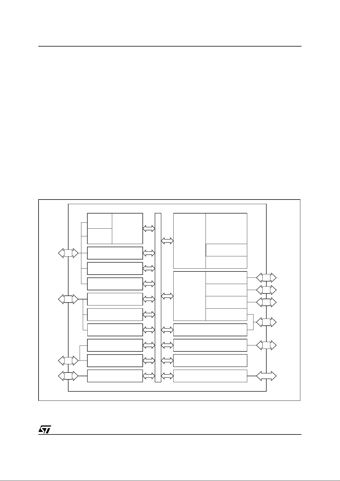
The uPSD323x Series combines a fast 8051based microcontroller with a flexible memory
structure, programmable logic, and a rich peripheral mix including USB, to form an ideal embedded
controller. At its core is an industry-standard 8032
MCU operating up to 40MHz.
A JTAG serial interface is used for In-System Programming (ISP) in as little as 10 seconds, perfect
for manufacturing and lab development.
The USB 1.1 low-speed interface has one Control
endpoint and two I nterrupt endpoints suitable f or
HID class drivers.
The 8032 core is coupled to Programmable System Device (PSD) architecture to optimize the
8032 memory structure, offering two independent
banks of Flash mem ory that can be pl aced at virtually any address within 8032 program or data address space, and easily paged beyond 64K bytes
using on-chip programmable decode logic.
Figure 2. Block Diagram
Dual Flash memory banks provide a robust solution for remote product updates in the field through
In-Application Programming (IAP). Dual Flash
banks also support EEPROM emulation, eliminating the need for exte r n al EEPROM chips.
General purpose programmable logic (PLD) is included to build an endless variety of glue-logic,
saving external logic devices. The PLD is conf igured using the software development tool, PSDsoft Express, available from the web at
www.st.com/psm, at no charge.
The uPSD323x also includes supervisor functions
such as a programmable watchdog timer and lowvoltage reset.
P3.0:7
P1.0:7
P4.0:7
USB+,
USB–
(3) 16-bit
Timer/
Counters
(2)
External
Interrupts
(8) GPIO, Port 3
(8) GPIO, Port 1
(4) 8-bit ADC
(5) 8-bit PWM
(8) GPIO, Port 4
I2C
UART0
UART1
USB v1.1
8032
MCU
Core
uPSD323x
Programmable
Programmable
SYSTEM BUS
1st Flash Memory:
128K or 256K Bytes
Decode and
Page Logic
General
Purpose
Logic,
16 Macrocells
8032 Address/Data/Control Bus
Watchdog and Low-Voltage Reset
VCC, VDD, GND, Reset, Crystal In
2nd Flash Memory:
32K Bytes
SRAM:
8K Bytes
(8) GPIO, Port A
(80-pin only)
(8) GPIO, Port B
(2) GPIO, Port D
(4) GPIO, Port C
JTAG ISP
(80-pin device only)
Supervisor:
PA0:7
PB0:7
PD1:2
PC0:7
MCU
Bus
Dedicated
Pins
AI10429
7/170
uPSD3234A, uPSD3234BV, uPSD3233B, uPSD3233BV
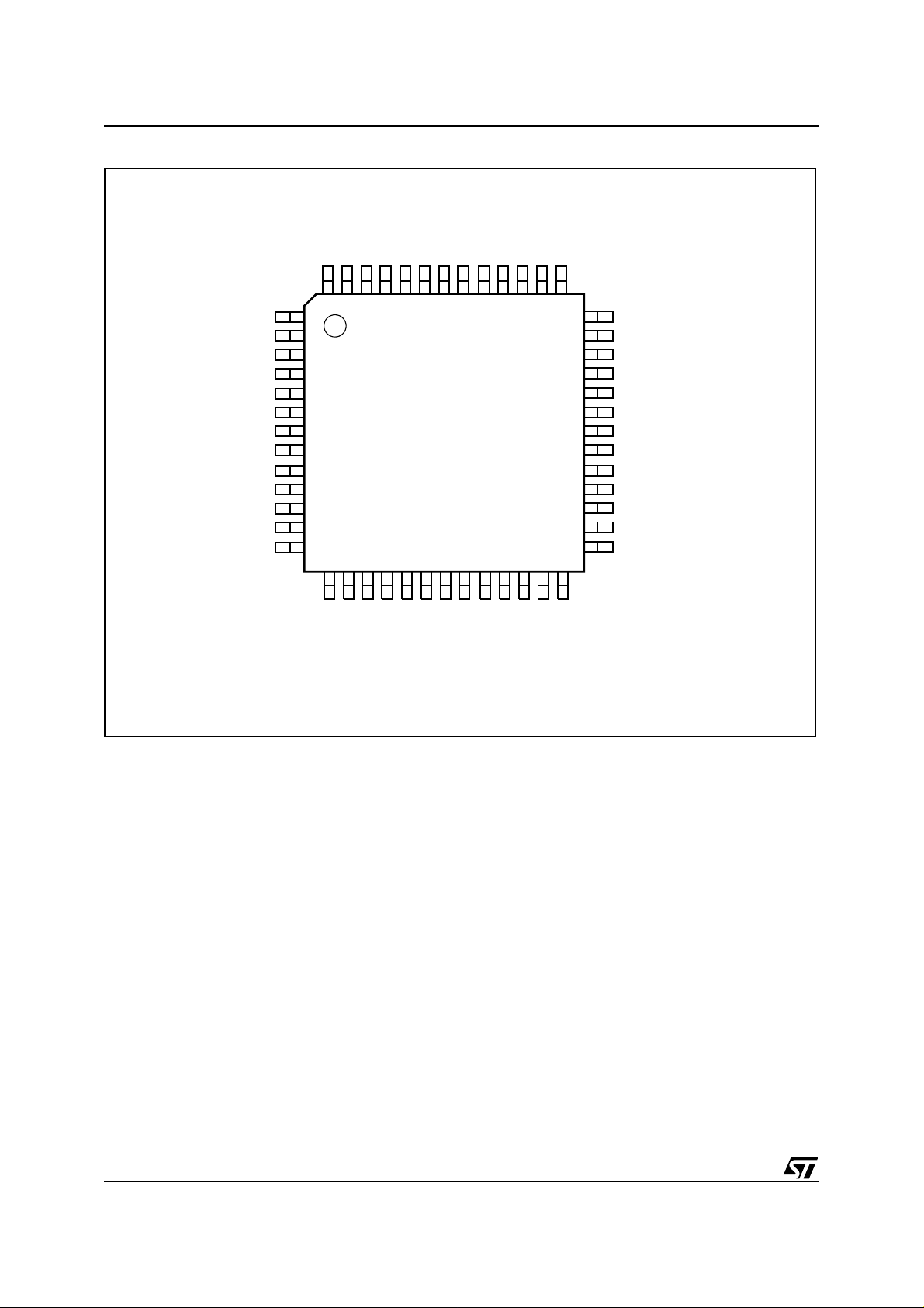
Figure 3. TQ FP 52 Connection s
PB0
PB1
PB2
PB3
PB4
PB5
VREF
GND
RESET_
PB6
PB7
52515049484746454443424140
P1.7/ADC3
P1.6/ADC2
PC7
(1)
USB+
V
CC
GND
STBY
1
2
3
4
5
6
7
8
9
10
11
12
13
14151617181920212223242526
P4.7/PWM4
P4.6/PWM3
P4.5/PWM2
P4.4/PWM1
GND
SYNC
P4.3/PWM0
P4.2/DDC V
P3.1/TXD
P3.0/RXD
P4.1/DDC SCL
P4.0/DDC SDA
P3.2/EXINT0
P3.3/EXINT1
39 P1.5/ADC1
38 P1.4/ADC0
37 P1.3/TXD1
36 P1.2/RXD1
35 P1.1/T2X
34 P1.0/T2
33 V
CC
32 XTAL2
31 XTAL1
30 P3.7/SCL1
29 P3.6/SDA1
28 P3.5/T1
27 P3.4/T0
AI07423b
PD1/CLKIN
JTAG TDO
JTAG TDI
USB–
PC4/TERR_
PC3/TSTAT
PC2/V
JTAG TCK
JTAG TMS
Note: 1. Pull-up re si stor re quired on pin 5 (2 k Ω for 3V devices, 7.5k Ω for 5V devices) for all 52-pi n devices, wi th or without USB function.
8/170
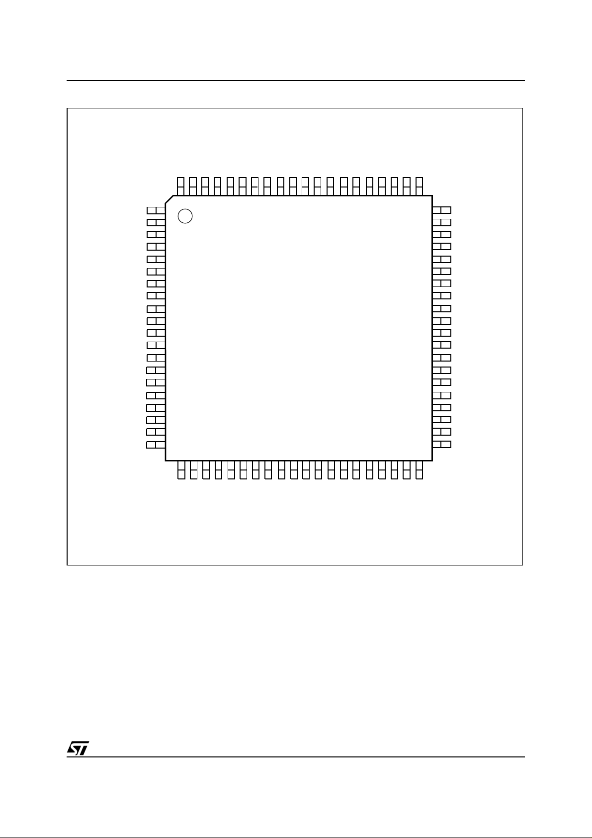
Figure 4. TQ FP 80 Connection s
PB0
P3.2/EXINT0
80797877767574737271706968676665646362
PD2
1
P3.3 /EXINT1
PD1/CLKIN
JTAG/TDO
JTAG/TDI
USB–
PC4/TERR_
PC3/TSTAT
PC2/V
JTAG TCK
P4.7/PWM4
P4.6/PWM3
JTAG TMS
ALE
PC7
(1)
USB+
(2)
NC
V
CC
GND
STBY
(2)
NC
2
3
4
5
6
7
8
9
10
11
12
13
14
15
16
17
18
19
20
PB1
P3.1/TXD0
uPSD3234A, uPSD3234BV, uPSD3233B, uPSD3233BV
(2)
PB2
P3.0/RXD0
PB3
PB4
PB5
NC
REF
V
GND
RESET_
PB6
PB7
RD_
P1.7/ADC3
PSEN_
WR_
P1.6/ADC2
61
60 P1.5/ADC1
59 P1.4/ADC0
58 P1.3/TXD1
57 A11
56 P1.2/RXD1
55 A10
54 P1.1/TX2
53 A9
52 P1.0/T2
51 A8
50 V
CC
49 XTAL2
48 XTAL1
47 AD7
46 P3.7/SCL1
45 AD6
44 P3.6/SDA1
43 AD5
42 P3.5/T1
41 AD4
21222324252627282930313233343536373839
PA7
PA6
PA5
PA4
P4.5/PWM2
P4.4/PWM1
P4.3/PWM0
Note: 1. Pull-up re si stor re quired on pin 8 (2 k Ω for 3V devices, 7.5k Ω for 5V devices) for all 82-pi n devices, wi th or without USB function.
2. NC = Not Connected
PA3
GND
SYNC
P4.2/DDC V
PA2
PA1
P4.1/DDC SCL
P4.0/DDC SDA
PA0
AD0
AD1
AD2
40
AD3
P3.4/T0
AI07424b
9/170

uPSD3234A, uPSD3234BV, uPSD3233B, uPSD3233BV
Table 2. 80-Pin Package Pin Description
Port Pin
Signal
Name
Pin No. In/Out
AD0 36 I/O
Basic Alternate
External Bus
Multiplexed Address/Data bus A1/D1
AD1 37 I/O Multiplexed Address/Data bus A0/D0
AD2 38 I/O Multiplexed Address/Data bus A2/D2
AD3 39 I/O Multiplexed Address/Data bus A3/D3
AD4 41 I/O Multiplexed Address/Data bus A4/D4
AD5 43 I/O Multiplexed Address/Data bus A5/D5
AD6 45 I/O Multiplexed Address/Data bus A6/D6
AD7 47 I/O Multiplexed Address/Data bus A7/D7
P1.0 T2 52 I/O General I/O port pin Timer 2 Count input
P1.1 TX2 54 I/O General I/O port pin Timer 2 Trigger input
P1.2 RxD1 56 I/O General I/O port pin 2nd UART Receive
P1.3 TxD1 58 I/O General I/O port pin 2nd UART Transmit
P1.4 ADC0 59 I/O General I/O port pin ADC Channel 0 input
P1.5 ADC1 60 I/O General I/O port pin ADC Channel 1 input
P1.6 ADC2 61 I/O General I/O port pin ADC Channel 2 input
P1.7 ADC3 64 I/O General I/O port pin ADC Channel 3 input
Function
A8 51 O External Bus, Address A8
A9 53 O External Bus, Address A9
A10 55 O External Bus, Address A10
A11 57 O External Bus, Address A11
P3.0 RxD0 75 I/O General I/O port pin UART Receive
P3.1 TxD0 77 I/O General I/O port pin UART Transmit
P3.2 EXINT0 79 I/O General I/O port pin
P3.3 EXINT1 2 I/O General I/O port pin
Interrupt 0 input / Timer 0 gate
control
Interrupt 1 input / Timer 1 gate
control
P3.4 T0 40 I/O General I/O port pin Counter 0 input
P3.5 T1 42 I/O General I/O port pin Counter 1 input
P3.6 SDA1 44 I/O General I/O port pin
P3.7 SCL1 46 I/O General I/O port pin
2
I
C Bus serial data I/O
2
I
C Bus clock I/O
P4.0 DDC SDA 33 I/O General I/O port pin
P4.1 DDC SCL 31 I/O General I/O port pin
P4.2
P4.3 PWM0 27 I/O General I/O port pin
DDC V
SYNC
30 I/O General I/O port pin
8-bit Pulse Width Modulation
output 0
10/170
uPSD3234A, uPSD3234BV, uPSD3233B, uPSD3233BV
Port Pin
P4.4 PWM1 25 I/O General I/O port pin
P4.5 PWM2 23 I/O General I/O port pin
P4.6 PWM3 19 I/O General I/O port pin
P4.7 PWM4 18 I/O General I/O port pin
Signal
Name
USB– 8 I/O
V
REF
RD_ 65 O READ signal, external bus
WR_ 62 O WRITE signal, external bus
PSEN_ 63 O PSEN
ALE 4 O Address Latch signal, external bus
RESET_ 68 I Active low RESET
XTAL1 48 I Oscillator input pin for system clock
XTAL2 49 O Oscillator output pin for system clock
Pin No. In/Out
Pull-up resistor required (2kΩ for 3V
devices, 7.5kΩ for 5V devices)
70 O Reference Voltage input for ADC
signal, external bus
Function
Basic Alternate
8-bit Pulse Width Modulation
output 1
8-bit Pulse Width Modulation
output 2
8-bit Pulse Width Modulation
output 3
Programmable 8-bit Pulse Width
modulation output 4
input
PA0 35 I/O General I/O port pin
PA1 34 I/O General I/O port pin
PA2 32 I/O General I/O port pin
PA3 28 I/O General I/O port pin
PA4 26 I/O General I/O port pin
PA5 24 I/O General I/O port pin
PA6 22 I/O General I/O port pin
PA7 21 I/O General I/O port pin
PB0 80 I/O General I/O port pin
PB1 78 I/O General I/O port pin
PB2 76 I/O General I/O port pin
PB3 74 I/O General I/O port pin
PB4 73 I/O General I/O port pin
PB5 72 I/O General I/O port pin
PB6 67 I/O General I/O port pin
PB7 66 I/O General I/O port pin
1. PLD Macro-cell outputs
2. PLD inputs
3. Latched Address Out (A0A7)
4. Peripheral I/O Mode
1. PLD Macro-cell outputs
2. PLD inputs
3. Latched Address Out (A0A7)
11/170

uPSD3234A, uPSD3234BV, uPSD3233B, uPSD3233BV
Port Pin
PC2
PC3 TSTAT 14 I/O General I/O port pin
PC4 TERR_ 9 I/O General I/O port pin
PC7 5 I/O General I/O port pin
PD1 CLKIN 3 I/O General I/O port pin
PD2 1 I/O General I/O port pin
Vcc 12
Vcc 50
GND 13
GND 29
GND 69
Signal
Name
JTAG TMS 20 I JTAG pin
JTAG TCK 16 I JTAG pin
V
STBY
JTAG TDI 7 I JTAG pin
JTAG TDO 6 O JTAG pin
USB+ 10
Pin No. In/Out
15 I/O General I/O port pin
Function
Basic Alternate
1. PLD Macro-cell outputs
2. PLD inputs
3. SRAM stand by voltage input (V
4. SRAM battery-on indicator
(PC4)
5. JTAG pins are dedicated
pins
1. PLD I/O
2. Clock input to PLD and APD
1. PLD I/O
2. Chip select to PSD Module
STBY
)
NC 11
NC 17
NC 71
52-PIN PACKAGE I/O PORT
The 52-pin package members of the uPSD323X
Devices have the sam e port pins as those of t he
80-pin package except:
■ Port 0 (P0.0-P0.7, external address/data bus
AD0-AD7)
■ Port 2 (P2.0-P2.3, external address bus A8-
A11)
■ Port A (PA0-PA7)
■ Port D (PD2)
■ Bus control signal (RD,WR,PSEN,ALE)
Pin 5 requires a pull-up resistor (2kΩ for 3V
devices, 7.5k Ω for 5V devices) for all devices,
with or without USB function.
12/170

uPSD3234A, uPSD3234BV, uPSD3233B, uPSD3233BV
ARCHITECTURE OVERVIEW
Memory Organization
The uPSD323X Devices’s standard 8032 Core
has separate 64KB address spac es for Program
memory and Data Memory. Program memory is
where the 8032 executes in structions from. Data
memory is used to hold data variables. Flash
memory can be mapped in either program or data
space. The Flash memory consists of two flash
memory blocks: the main Flash (1 or 2Mbit) and
the Secondary Flash (256Kbit). Except during
flash memory programming or update, Flash
memory can only be read, not written to. A Page
Register is used to access memory beyond the
64K bytes address space. Refer to the PSD Module for details on mapping of the Flash memory.
Figure 5. Memory Map and Address Space
MAIN
FLASH
The 8032 core h as t wo t ypes of data memory (internal and external) that can be read and written.
The internal SRAM consists o f 256 byte s, and includes the stack area.
The SFR (Special Function Registers) occupies
the upper 128 bytes of the internal SRAM, the registers can be accessed by Direct addressing only.
There are two separate blocks of external SRAM
inside the uPSD323X Devices: one 256 bytes
block is assigned for DDC data storage. Anot her
8K bytes resides in the PSD Modu le that can be
mapped to any address space defined by the user.
EXT. RAM
INT. RAM
SECONDARY
FLASH
32KB
Flash Memory Space
128KB
OR
256KB
FF
Indirect
Addressing
7F
Indirect
Direct
Addressing
0
Internal RAM Space
(256 Bytes)
or
Registers
The 8032 has several registers; these are the Program Counter (PC), Accumulator (A), B Register
(B), the Stack Pointer (SP), the Program Status
Word (PSW), General purpose registers (R0 to
R7), and DPTR (Data Pointer register).
EXT. RAM
FFFF
FF00
(DDC)
External RAM Space
(MOVX)
SFR
Direct
Addressing
Figure 6. 8032 MCU Registers
A
B
SP
PCH
DPTR(DPH)
PCL
PSW
R0-R7
DPTR(DPL)
8KB256B
AI06635
Accumulator
B Register
Stack Pointer
Program Counter
Program Status Word
General Purpose
Register (Bank0-3)
Data Pointer Register
AI06636
13/170
uPSD3234A, uPSD3234BV, uPSD3233B, uPSD3233BV
Accumulator. The Accumulator is the 8-bit gen-
eral purpose register, used for data operation such
as transfer, temporary saving, and conditional
tests. The Accumulator can be used as a 16-bit
register with B Register as shown below.
Figure 7. Configuration of BA 16-bit Registers
B
AB
A
Two 8-bit Registers can be used as a "BA" 16-bit Registers
AI06637
B Register. The B Register is the 8-bit general
purpose register, used for an arithmetic operation
such as multiply, division with Accumulator
Stack Pointer. The Stack Pointer Register is 8
bits wide. It is incremented before data is stored
during PUSH and CALL executions. While the
stack may reside anywhere in on-chip RAM, the
Stack Po inter is in itializ ed to 07 h a fter res et. T his
causes the stack to begin at location 08h.
Figure 8. Stack Pointer
Stack Area (30h-FFh)
Bit 15 Bit 0Bit 8 Bit 7
Hardware Fixed
SP (Stack Pointer) could be in 00h-FFh
SP00h
00h-FFh
AI06638
Program Counter. The Program Counter is a 16bit wide which consists of two 8-bit registers, PCH
and PCL. This counter indicates the address of the
next instruction to be executed. In RESET
state,
the program counter has reset routine address
(PCH:00h, PCL:00h).
Program Status Word. The Program Status
Word (PSW) contains several bits that reflect the
current state of the CPU and select Internal RAM
(00h to 1Fh: Bank0 to Bank3). The PSW is described in Figure 9., page 15. It contains the Carry
flag, the Auxiliary carry flag, the Half Carry (for
BCD operation), the general purpose flag, the
Register bank select flags, the Overflow flag, and
Parity flag .
[Carry Flag, CY]. This flag stores any carry or not
borrow from the ALU of CPU after an arithmetic
operation and is also changed by the Shift Instruction or Rotate Instruction.
[Auxiliary Carry Flag, AC]. After operation, this is
set when there is a carry from Bit 3 of ALU or there
is no borrow from Bit 4 of ALU.
[Register Bank Select Flags, RS0, RS1]. This flags
select one of four bank(00~07H:bank0,
08~0Fh:bank1, 10~17h: bank2, 17~1Fh:bank3) in
Internal RAM.
[Overflow Flag, OV]. This flag is set to '1' when an
overflow occurs as the result of an arithmetic operation involving signs. An overflow occurs when the
result of an addition or subtraction exceeds +127
(7Fh) or -128 (80h). The CLRV instruction clears
the overflow flag. There is no set instruction. When
the BIT instruction is executed, Bit 6 of memory is
copied to this flag.
[Parity Flag, P]. This flag reflect on number of Accumulator’s 1. If number of Accumulator’s 1 is odd,
P=0. otherwise P=1. Sum of adding Accumulator’s
1 to P is always even.
R0~R7. General purpose 8-bit registers that are
locked in the lower portion of internal data area.
Data Pointer Register. Data Pointer Register is
16-bit wide which consists of two-8bit registers,
DPH and DPL. This register is used as a data
pointer for the data transmission with external data
memory in the PSD Module.
14/170

uPSD3234A, uPSD3234BV, uPSD3233B, uPSD3233BV
Figure 9. PSW (Program Stat us W o rd) Re gi st er
MSB
CY
PSW
Carry Flag
Auxillary Carry Flag
General Purpose Flag
AC FO RS1RS0 OV P
Register Bank Select Flags
(to select Bank0-3)
Program Memory
The program memory consists of two Flash memory: 128 KByte (or 256 KByte) Main Flash and 32
KByte of Secondary Flash. The Flash memory can
be mapped to any address space as defined by
the user in the PSDsoft Tool. It can also be
mapped to Data memory space during Flash
memory update or programming.
After reset, the CPU begins execution from location 0000h. As shown in Figure 10, e ach interrupt
is assigned a fixed location in Program Memory.
The interrupt causes the CPU to jump to that location, where it commences execution of the service
routine. External Interrupt 0, for example, is assigned to location 0003h. If External Interrupt 0 is
going to be used, its service routine must begin at
location 0003h. If the interrupt is not going to be
used, its service location is available as gen eral
purpose Pro-gram Memory.
The interrupt service locations are spaced at 8byte intervals: 0003h for External Interrupt 0,
000Bh for Timer 0, 0013 h for E xternal I nterrupt 1,
001Bh for Timer 1 and so forth. If an interrupt service routine is short enough (as is often the cas e
in control applications), it can reside entirely within
that 8-byte interval. Longer service routines can
use a jump instruction to skip over subsequent interrupt locations, if other interrupts are in use.
Data memory
The internal data memory is divided into four physically separ ated blocks: 256 byt es of internal RAM,
128 bytes of Special Function Registers (SFRs)
areas, 256 bytes of external RAM (XRAM-DDC)
and 8K bytes (XRAM-PSD) in the PSD Module.
RAM
Four register banks, each 8 registers wide, occupy
locations 0 through 31 in the lower RAM area.
Only one of these banks may be enabled at a time.
The next 16 bytes, locations 32 through 47, contain 128 directly addressable bit locations. The
stack depth is only limited by the available internal
RAM space of 256 bytes.
LSB
Reset Value 00h
Parity Flag
Bit not assigned
Overflow Flag
AI06639
Figure 10. Int errupt Locatio n of Program Memory
008Bh
•
•
•
•
0013h
000Bh
0003h
0000hReset
8 Bytes
AI06640
Interrupt
Location
•
•
•
•
•
XRAM-DDC
The 256 bytes of XRAM-DDC used to support
DDC interface is also available for system usage
by indirect addressing through the address pointer
DDCADR and data I/O buffer RAMBUF. The address pointer (DDCADR) is equipped with the post
increment capability to facilitate the transfer of
data in bulk (for details refer to DDC Interface
part). However, it is also possible to address t he
RAM through MOVX comm and as normally used
in the internal RAM extension of 80C51 derivatives. XRAM-DDC FF00 to FFFF is directly addressable as external data memory locations
FF00 to FFFF via MOVX-DPTR inst ruction or via
MOVX-Ri instruction. When XRAM-DDC is disabled, the address space FF00 to FFFF can be assigned to other resources.
XRAM-PSD
The 8K bytes of XRAM-PS D resides in the PSD
Module and can be mapped to any address space
through the DPLD (Decoding PLD) as defined by
the user in PSDsoft Development tool. The XRAMPSD has a battery backup feature that allow the
data to be retained in t he event of a power lost.
The battery is connected t o the Port C PC2 pin.
This pin must be configured in PSDSoft to be battery back-up.
15/170

uPSD3234A, uPSD3234BV, uPSD3233B, uPSD3233BV
SFR
The SFRs can only be addressed directly in the
address range from 80h to FFh. Table
15., page 28 gives an overview of the Special
Function Registers. Sixteen address in the SFRs
space are both-byte and bit-addressable. Th e bi taddressable SFRs are those whose address ends
in 0h and 8h. The bit addresses in this area are
80h to FFh.
Addressing Modes
The addressing modes in uPSD323X Devices instruction set are as follows
■ Direct addressing
■ Indirect addressing
■ Register addressing
■ Register-specific addressing
■ Immediate constants addressing
■ Indexed addressing
Table 3. RAM Address
Byte Address
(in Hexadecimal)
↓↓
FFh 255
30h 48
msb Bit Address (Hex) lsb
Byte Address
(in Decimal)
(1) Direct addressing. In a direct addressing the
operand is specified by an 8-bit address field in the
instruction. Only internal Data RAM and SFRs
(80~FFH RAM) can be directly addressed.
Example:
mov A, 3EH ; A <----- RAM[3E]
Figure 11. Direct Addressing
2Fh 7F 7E 7D 7C 7B 7A 79 78 47
2Eh777675747372717046
2Dh 6F 6E 6D 6C 6B 6A 69 68 45
2Ch676665646362616044
Program Memory
3Eh
04
A
2Bh 5F 5E 5D 5C 5B 5A 59 58 43
2Ah575655545352515042
29h 4F 4E 4D 4C 4B 4A 49 48 41
28h 47 46 45 44 43 42 41 40 40
27h 3F 3E 3D 3C 3B 3A 39 38 39
26h 37 36 35 34 33 32 31 30 38
25h 2F 2E 2D 2C 2B 2A 29 28 37
24h 27 26 25 24 23 22 21 20 36
23h 1F 1E 1D 1C 1B 1A 19 18 35
22h 17 16 15 14 13 12 11 10 34
21h 0F 0E 0D 0C 0B 0A 09 08 33
20h 07 06 05 04 03 02 01 00 32
1Fh
Register Bank 3
18h 24
17h
Register Bank 2
10h 16
0Fh
Register Bank 1
08h 8
07h
Register Bank 0
00h 0
31
23
15
7
AI06641
(2) Indirect addressing. In indirect addressing
the instruction specifies a register which cont ains
the address of the operand. Both internal and external RAM can be indirectly addressed. The address register for 8-bit addresses can be R0 or R1
of the selected register bank, or the Stack Pointer.
The address register for 16-bit addresses can only
be the 16-bit “data pointer” register, DPTR.
Example:
mov @R1, #40 H ;[R1] <-----40H
Figure 12. Indi rect Address in g
Program Memory
55h
R1
40h
55
AI06642
16/170
uPSD3234A, uPSD3234BV, uPSD3233B, uPSD3233BV
(3) Register addressing. The register banks,
containing registers R0 through R7, can be accessed by certain instruction s which carry a 3-bit
register specification within the o pcode of the instruction. Instructions that access the registers
this way are code efficient, since this m ode eliminates an address byte. When the instruction is executed, one of four banks is selected at execution
time by the two bank select bits in the PSW.
Example:
mov PSW, #0001000B ; select Bank0
mov A, #30H
mov R1, A
(4) Register-specific addressing. Some instructions are specific to a certain register. For example, some instructions always operate on the
Accumulator, or Data Pointer, etc., so no addres s
byte is needed to point it. The opcode it self does
that.
(5) Immediate constants addressing. The value of a constant can follow the opcode in Program
memory.
Example:
mov A, #10H.
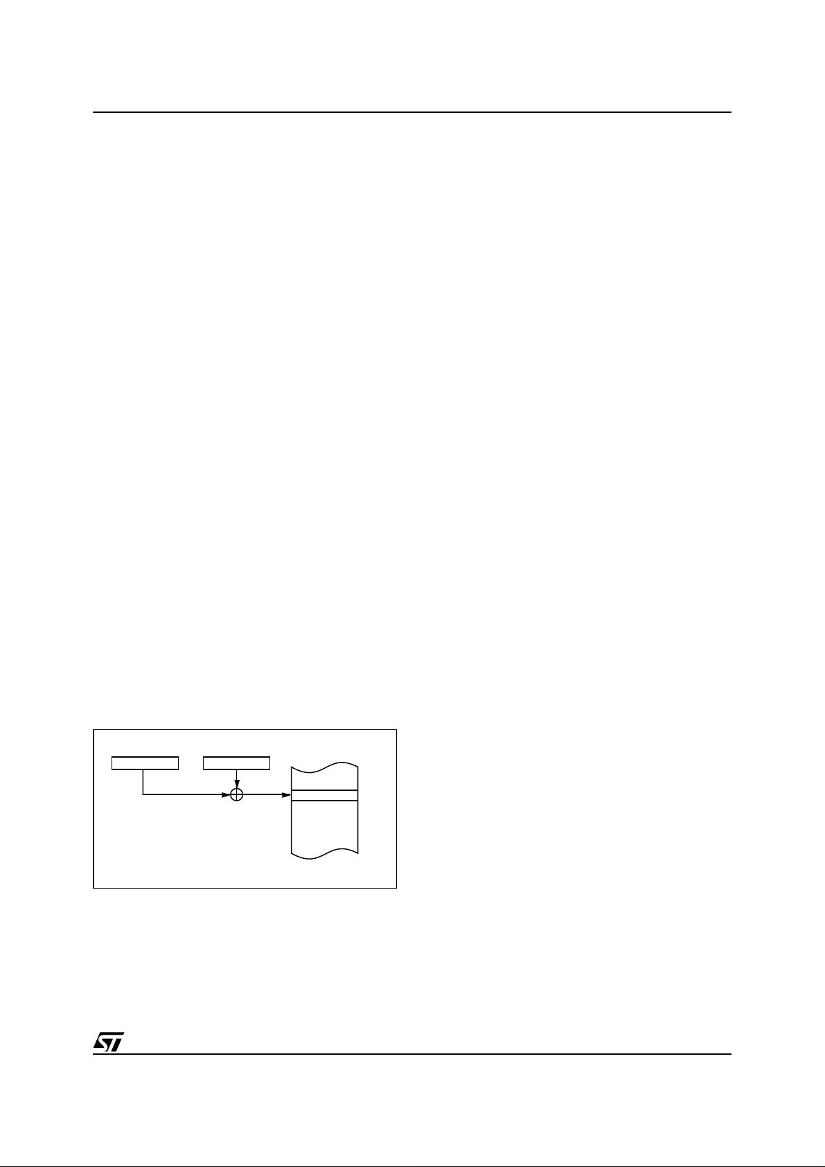
(6) Indexed addressing. Only Program me mory
can be accessed with indexed addressing, a nd it
can only be read. This addressing mode is intended for reading look-up tables in Program memory.
A 16-bit base register (either DPTR or PC) points
to the base of the table, and the Accumulator is set
up with the table entry number. The address of the
table entry in Program memory is formed by adding the Accumulator data to the base pointer.
Example:
movc A, @A+DPTR
Figure 13. Indexed Addre ssing
ACC DPTR
3Ah 1E73h
Program Memory
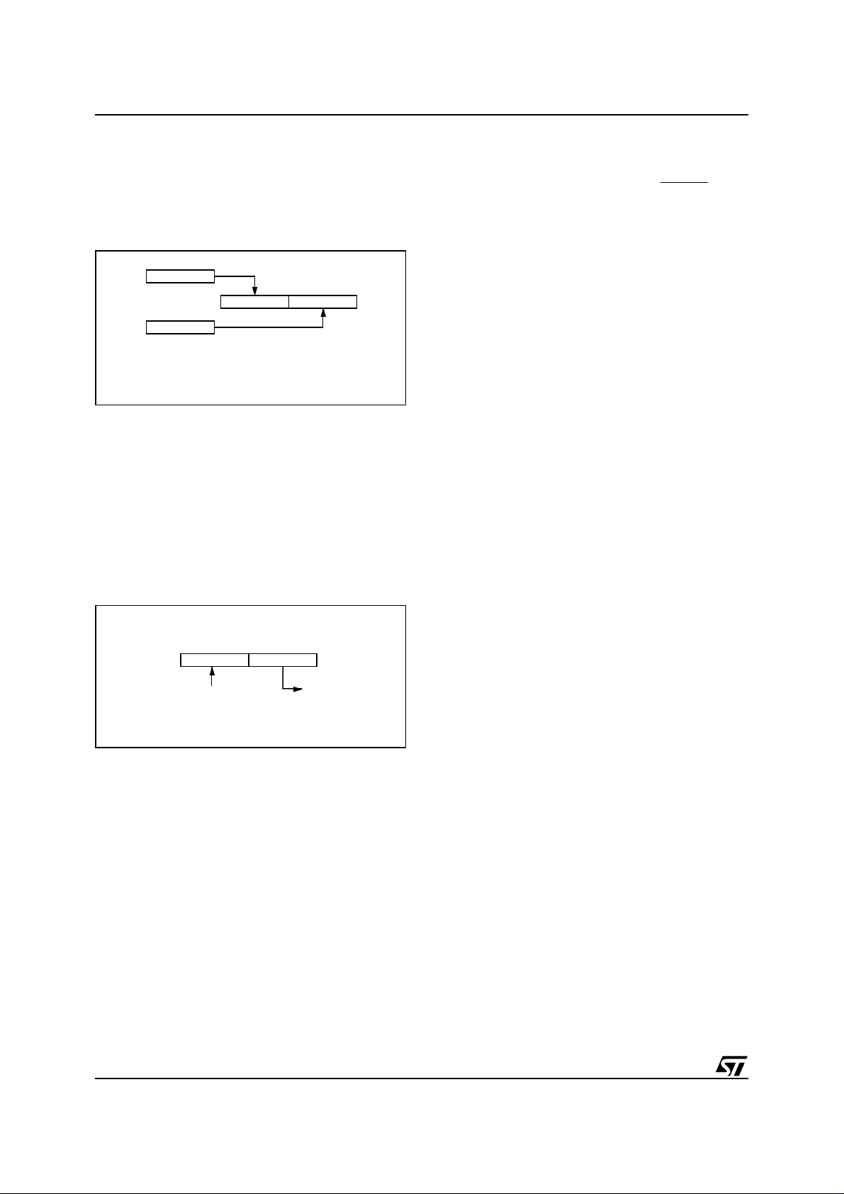
Arithmetic Instructions
The arithmetic instructions is listed in Table
4., page 18. The table indicates the addressing
modes that can be used with each i nstruction to
access the <byte> operand. For example, the
ADD A, <byte> instruction can be written as:
ADD a, 7FH (direct addressing)
ADD A, @R0 (indirect addressing)
ADD a, R7 (register addressing)
ADD A, #127 (immediate constant)
Note: Any byte in the internal Data Memory space
can be incremented without going through the Accumulator.
One of the INC instructions operates on the 16-bit
Data Pointer. The Data Pointer is used to generate
16-bit addresses for external memory, so being
able to increment it in one 16-bit operations is
a useful feature.
The MUL A B instruc tion mul tiplies the Accum ula-
tor by the data in the B register and puts the 16-bit
product into the concatenated B and Acc um ulator
registers.
The DIV AB instruction divides the Accumulator by
the data in the B register and leaves the 8-bit quotient in the Accumulator, and the 8-bit remainder in
the B regi ste r.
In shift operations, dividing a num ber by 2n s hifts
its “n” bits to the right. Using DIV AB t o perform the
division completes the shift in 4?s and leaves the
B register holding the b its that were shifted out.
The DAA instruction is for BCD arithmetic operations. In BCD arithmetic, ADD and ADDC instructions should always be followed by a DAA
operation, to ensure that the result is also in BCD.
Note: DAA will not convert a binary number to
BCD. The DAA operation produces a meaningful
result only as the second step in the addition of
two BCD bytes.
AI06643
3Eh
17/170

uPSD3234A, uPSD3234BV, uPSD3233B, uPSD3233BV
Table 4 . Arithm etic Instructio n s
Mnemonic Operation
ADD A,<byte> A = A + <byte> X X X X
ADDC A,<byte> A = A + <byte> + C X X X X
SUBB A,<byte> A = A – <byte> – C X X X X
INC A = A + 1 Accumulator only
INC <byte> <byte> = <byte> + 1 X X X
INC DPTR DPTR = DPTR + 1 Data Pointer only
DEC A = A – 1 Accumulator only
DEC <byte> <byte> = <byte> – 1 X X X
MUL AB B:A = B x A Accumulator and B only
DIV AB
DA A Decimal Adjust Accumulator only
A = Int[ A / B ]
B = Mod[ A / B ]
Dir. Ind. Reg. Imm
Logical Instructions
Table 5., page 19 shows list of uPSD323X Devic-
es logical instructions. The instructions that perform Boolean operations (AND, OR, Exclusive
OR, NOT) on bytes perform the operation on a bitby-bit basis. That is, if th e Accumulator contains
00110101B and byte contains 01010011B, then:
ANL A, <byte>
will leave the Accum u lator holdi ng 00010001B.
The addressing modes that can be used to access
the <byte> operand are listed in Table 5., page 19.
The ANL A, <byte> instruction may take any of the
forms:
ANL A,7FH(direct addressing)
ANL A, @R1 (indirect addressing)
ANL A,R6 (register addressing)
ANL A,#53H (immediate constant)
Note: Boolean operations can be performed on
any byte in the internal Data Mem ory space without going through the Accumulator. The XRL
<byte>, #data instruction, for example, offers a
quick and easy way to invert port bits, as in
If the operation is in response to an interrupt, not
using the Accumulator saves the time and effort to
push it onto the stack in the service routine.
The Rotate instructions (RL A , RLC A, etc.) shift
the Accumulator 1 bit to the left or right. For a left
rotation, the MSB rolls into the LSB position. For a
right rotation, the LSB rolls into the MSB position.
The SWAP A instruction interchanges the high
and low nibbles within the Accumulator. This is a
useful operation in BCD manipulations. For example, if the Accumulator contains a binary num ber
which is known to be less than 100, it can be quickly converted to BCD by the following code:
MOVE B,#10
DIV AB
SWAP A
ADD A,B
Dividing the number by 10 leaves the tens digit in
the low nibble of the Acc umulator, and the ones
digit in the B register. The SWAP and ADD instructions move the tens digit to the high nibble of the
Accumulator, and the ones digit to the low nibble.
XRL P1, #0FFH.
Addressing Modes
Accumulator and B only
18/170
uPSD3234A, uPSD3234BV, uPSD3233B, uPSD3233BV
Table 5. Logical Instructions
Mnemonic Operation
Dir. Ind. Reg. Imm
ANL A,<byte> A = A .AND. <byte> X X X X
ANL <byte>,A A = <byte> .AND. A X
ANL <byte>,#data A = <byte> .AND. #data X
ORL A,<byte> A = A .OR. <byte> X X X X
ORL <byte>,A A = <byte> .OR. A X
ORL <byte>,#data A = <byte> .OR. #data X
XRL A,<byte> A = A .XOR. <byte> X X X X
XRL <byte>,A A = <byte> .XOR. A X
XRL <byte>,#data A = <byte> .XOR. #data X
CRL A A = 00h Accumulator only
CPL A A = .NOT. A Accumulator only
RL A Rotate A Left 1 bit Accumulator only
RLC A Rotate A Left through Carry Accumulator only
RR A Rotate A Right 1 bit Accumulator only
Addressing Modes
RRC A Rotate A Right through Carry Accumulator only
SWAP A Swap Nibbles in A Accumulator only
19/170
uPSD3234A, uPSD3234BV, uPSD3233B, uPSD3233BV
Data Transfers
Internal RAM. Table 6 shows the menu of in-
structions that are available for moving data
around within the internal memory spaces, and the
addressing modes that can be used with each
one. The MOV <dest>, <src> instruction allows
data to be transferred between any two internal
RAM or SFR locations without going through the
Accumulator. Remember, the Uppe r 128 b ytes of
data RAM can be accessed only by indirect addressing, and SFR space only by di rect addressing.
Note: In uPSD323X Devices, the stack resides in
on-chip RAM, and grows upwards. T he PUSH instruction first increments the Stac k Pointer (SP),
then copies the byte into the stack. PUSH and
POP use only direct addressing to identify the byte
being saved or restored, but the stack itself is accessed by indirect addressing using the S P register. This means the stack can go into the Upper
128 bytes of RAM, if they are implemented, but not
into SFR space.
The Data Transfer instructions include a 16-bit
MOV that can be used to initialize the Data Pointer
(DPTR) for look-up tables in Program Memory.
The XCH A, <byte> instruction causes the Accumulator and ad-dressed byte to exchange data.
The XCHD A, @Ri instruction is similar, but only
the low nibbles are involved in the exchange. To
see how XCH and XCHD can be used to facilitate
data manipulations, consider first the problem of
shifting and 8-digit BCD number two digits to the
right. Table 8., page 21 shows how this can be
done using XCH instructions. To aid in understanding how the code works, the contents of the
registers that are holding the BCD number and the
content of the Accumulator are shown alon gside
each instruction to indicate their status after the instruction has been executed.
After the routine has been executed, the Accumulator contains the two digits that were shifted out
on the right. Doing the routine with direct MOVs
uses 14 code bytes. The same operation with
XCHs uses only 9 bytes and executes almost
twice as fast. To right-shift by an odd number of
digits, a one-digit must be executed. Table
9., page 21 shows a sample of code that will right-
shift a BCD number one digit, using the XCHD instruction. Again, the contents of the registers holding the number and of the accumulator are shown
alongside each instruction.
Table 6. Data Transfer Instructions that Access Internal Data Memory Space
Mnemonic Operation
Dir. Ind. Reg. Imm
MOV A,<src> A = <src> XXXX
MOV <dest>,A <dest> = A X X X
MOV <dest>,<src> <dest> = <src> XXXX
MOV DPTR,#data16 DPTR = 16-bit immediate constant X
PUSH <src> INC SP; MOV “@SP”,<src> X
POP <dest> MOV <dest>,”@SP”; DEC SP X
XCH A,<byte> Exchange contents of A and <byte> X X X
XCHD A,@Ri Exchange low nibbles of A and @Ri X
Addressing Modes
20/170
uPSD3234A, uPSD3234BV, uPSD3233B, uPSD3233BV
First, pointers R1 and R0 are set up to point to the
two bytes containing the last four BCD digits. Then
Table 7. Shifting a BCD Number Two Digits to the Right (using direct MOVs: 14 bytes)
a loop is executed which leaves the last byte, location 2EH, holding the l ast two dig its of the s hifted
number. The pointers are decremented, and the
loop is repeated for location 2DH. The CJNE instruction (Compare and Jump if Not equal) is a
loop control that will be des cribed later. The loop
MOV A,2Eh 00 12 34 56 78 78
MOV 2Eh,2Dh 00 12 34 56 56 78
MOV 2Dh,2Ch 00 12 34 34 56 78
executed from LOOP to CJNE for R1 = 2EH, 2DH,
2CH, and 2BH. At that point the digit that was originally shifted out on the right has propagated to location 2AH. Since that location should be left with
MOV 2Ch,2Bh 00 12 12 34 56 78
MOV2Bh,#0 0000123456 78
0s, the lost digit is moved to the Accumulator.
Table 8. Shifting a BCD Number Two Digits to the Right (using direct XCHs: 9 bytes)
CLR A 00 12 34 56 78 00
XCH A,2Bh 00 00 34 56 78 12
XCH A,2Ch 00 00 12 56 78 34
XCH A,2Dh 00 00 12 34 78 56
XCH A,2Eh 00 00 12 34 56 78
Table 9. Shifting a BCD Number One Digit to the Right
2A 2B 2C 2D 2E ACC
MOV R1,#2Eh 00 12 34 56 78 xx
MOV R0,#2Dh 00 12 34 56 78 xx
2A 2B 2C 2D 2E ACC
2A 2B 2C 2D 2E ACC
; loop for R1 = 2Eh
LOOP:MOV A,@R1 0012345678 78
XCHD A,@R0 0012345878 76
SWAP A 00 12 34 58 78 67
MOV @R1,A 00 12 34 58 67 67
DEC R1 0012345867 67
DEC R0 0012345867 67
CNJE R1,#2Ah,LOOP 00 12 34 58 67 67
; loop for R1 = 2Dh 00 12 38 45 67 45
; loop for R1 = 2Ch 00 18 23 45 67 23
; loop for R1 = 2Bh 08 01 23 45 67 01
CLR A 08 01 23 45 67 00
XCH A,2Ah 00 01 23 45 67 08
21/170
uPSD3234A, uPSD3234BV, uPSD3233B, uPSD3233BV
External RAM. Table 10 shows a l ist of the Data
Transfer instructions that access external Data
Memory. Only indirect addressing can be used.
The choice is whether to us e a one-by te address,
@Ri, where Ri can be either R0 or R1 of the s elected register bank, or a two-byte
address, @DTPR.
Note: In all external Data RAM accesses, the Accumulator is always either the destination or
source of the data.
Lookup Tables. Table 11 shows the two instruc-
tions that are available for reading lookup tables in
Program Memory. Since these instructions access
only Program Memory, the lookup tables can only
be read, not updated.
The mnemonic is MOVC for “move constant.” The
first MOVC instruction in Table 11 can accommo-
date a table of up to 256 entries numbered 0
through 255. The number of th e desired entry is
loaded into the Accumulator, and the Data Pointer
is set up to point to the beginning of the table.
Then:
MOVC A, @A+DPTR
copies the desired table entry into the Accumula-
tor.
The other MOVC instruction works the same way,
except the Program Counter (PC) is used as the
table base, and the table is accessed th rough a
subroutine. First the number of the desired en-try
is loaded into the Accumulator, and the subroutine
is called:
MOV A , ENTRY NUMBER
CAL L TAB LE
The subroutine “TABLE” would look like this:
TABLE: MO VC A , @ A+PC
RET
The table itself immediately follows the RET (return) instruction is Program Memory. This type of
table can have up to 255 entries, numbered 1
through 255. Number 0 cannot b e used, because
at the time the MOVC instruction is executed, the
PC contains the address of the RET instru ction.
An entry numbered 0 would be the RET opcode itself.
Table 10. Data Transfer Instruction that Access External Data Memory Space
Address Width Mnemonic Operation
8 bits MOVX A,@Ri READ external RAM @Ri
8 bits MOVX @Ri,A WRITE external RAM @Ri
16 bits MOVX A,@DPTR READ external RAM @DPTR
16 bits MOVX @DPTR,a WRITE external RAM @DPTR
Table 11. Lookup Table READ Instruction
Mnemonic Operation
MOVC A,@A+DPTR READ program memory at (A+DPTR)
MOVC A,@A+PC READ program memory at (A+PC)
22/170

uPSD3234A, uPSD3234BV, uPSD3233B, uPSD3233BV
Boolean Instructions
The uPSD323X Devices contain a complete Boolean (single-bit) processor. One page o f the internal RAM contains 128 address -able bits, and the
SFR space can support up to 128 addressable bits
as well. All of the port lines are bit-addressable,
and each one can be treated as a separate singlebit port. The instructions that access these bits are
not just conditional branches, but a complete
menu of move, set, clear, complement, OR and
AND instructions. These kinds of bit operations
are not easily obtained in other architectures with
any amount of byte-oriented software.
The instruction set for the Boolean processor is
shown in Table 12. All bits acces ses are by di re ct
addressing.
Bit addresses 00h through 7Fh are i n the Lower
128, and bit ad-dresses 80h through FFh are in
SFR space.
Note how easily an internal flag can be moved to
a port pin:
MOV C,FLAG
MOV P1.0 ,C
In this example, FLAG is the name of any addressable bit in the Lower 128 or SFR space. An I/O
line (the LSB of Port 1, in this case) is set or
cleared depending on whether the Flag Bit is '1' or
'0.'
The Carry Bit in the PSW is used as the single-bit
Accumulator of the Boolean processor. Bit instructions th at re fer to th e Ca rr y B it as C as se mbl e a s
Carry-specific instructions (CLR C, etc.). The Carry Bit also has a direct address, since it resides in
the PSW register, which is bit-addressable.
Note: The Boolean instruction set includes ANL
and ORL operations, but not the XRL (Exclusive
OR) operation. An XRL operation is simple to implement in software. Suppose, for example, it is required to form the Exclusive OR of two bits:
C = bit 1 .XRL. bit2
The software to do that could be as follows:
MOV C , bit1
JNB bit2, OVER
CPL C
OVER: (continue)
First, Bit 1 is moved to the Carry. If bit2 = 0, then
C now contains the correct result. That is, Bit 1
.XRL. bit2 = bit1 if bit2 = 0. On the o ther hand, if
bit2 = 1, C now contains the complement of the
correct result. It need only be inverted (CPL C) to
complete the operation.
This code uses the JNB instruction, one of a series
of bit-test instructions which execute a jump if the
addressed bit is set (JC, JB, JBC) or if the addressed bit is not set (JNC, JNB). In the above
case, Bit 2 is being tested, and if bit2 = 0, the CPL
C instruction is jumped over.
JBC executes the jump if the addressed bit is set,
and also clears the bit. Thus a flag can be tested
and cleared in one operation. All the PSW bits are
directly addressable, so the P arity B it, or the general-purpose flags, for example, are also available
to the bit-test instructions.
Table 12. Boolean Instructions
Mnemonic Operation
ANL C,bit C = A .AND. bit
ANL C,/bit C = C .AND. .NOT. bit
ORL C,bit C = A .OR. bit
ORL C,/bit C = C .OR. .NOT. bit
MOV C,bit C = bit
MOV bit,C bit = C
CLR C C = 0
CLR bit bit = 0
SETB C C = 1
SETB bit bit = 1
CPL C C = .NOT. C
CPL bit bit = .NOT. bit
JC rel Jump if C =1
JNC rel Jump if C = 0
JB bit,rel Jump if bit =1
JNB bit,rel Jump if bit = 0
JBC bit,rel Jump if bit = 1; CLR bit
Relative Offset
The destination address for these jum ps is specified to the assembler by a label or by an actual address in Program memory. How-ever, the
destination address assembl es to a relative off set
byte. This is a signed (two’s complement) offset
byte which is added to the PC in two’s complement
arithmetic if the jump is executed.
The range of the jump is therefore -128 to +127
Program Memory bytes relative to the first byte following the instruction.
23/170

uPSD3234A, uPSD3234BV, uPSD3233B, uPSD3233BV
Jump Instructions
Table 13 shows the list of unconditional jump instructions. The table lists a single “JMP add” instruction, but in fact there a re thre e SJ MP, LJ M P,
and AJMP, which differ in the format of the destination address. JMP is a generic mnemonic which
can be used if the programmer does not care
which way the jump is en-coded.
The SJMP instruction encodes the destination address as a relative offset, as described above. The
instruction is 2 bytes long, consisting of the opcode and the relative offset byte. The jump distance is limited to a range of -128 to +127 bytes
relative to the instruction following the SJMP.
The LJMP instruction encodes the destination address as a 16-bit constant. The instruction is 3
bytes long, consisting o f the op code and two address bytes. The des tination address can be anywhere in the 64K Program Memory space.
The AJMP instruction encodes the destination address as an 11-bit constant. The instruction is 2
bytes long, consisting of the opcode, which itself
contains 3 of the 11 address bits, followed by another byte containing the low 8 bits of the destination address. When the instruction is executed,
these 11 bits are simply substituted for the low 11
bits in the PC. The high 5 bits stay the same.
Hence the destination has to be within the same
2K block as the instruction following the AJMP.
In all cases the programmer specifies the destination address to the assembler in the same way: as
a label or as a 16-bit constant. The assembler will
put the destination address into the correct format
for the given instruction. If the format required by
the instruction will not support t he distance t o the
specified destination add ress, a “Destination out
of range” message is written into the List file.
The JMP @A+DPTR instruction supports case
jumps. The destination address is computed at execution time as the sum of the 16-bit DPTR register and the Accumulator. Typically. DPTR is set up
with the address of a jump table. In a 5-way
branch, for ex-ample, an integer 0 through 4 is
loaded into the Accumulator. The c ode to be executed mi ght be as fo llows:
MOV DPTR,#JUMP TABLE
MOV A,INDEX_NUMBER
RL A
JMP @A+DPTR
The RL A instruction converts the index number (0
through 4) to an even number on the range 0
through 8, because each entry in the jump table is
2 bytes long:
JUMP TABLE:
AJMP CASE 0
AJMP CASE 1
AJMP CASE 2
AJMP CASE 3
AJMP CASE 4
Table 13 s hows a single “CALL addr” instruction,
but there are two of them, LCALL and ACALL,
which differ in the format in which the subroutine
address is given to the CPU. CALL is a generic
mnemonic which can b e used if the programm er
does not care which way the address is encoded.
The LCALL instruction uses the 16-bit address format, and the subroutine can be anywh ere in the
64K Program Memory space. The ACALL instruction uses the 11-bit format, and the subroutine
must be in the same 2K block as the instruction following the ACALL.
In any case, the programmer specifies the subroutine address to the assembler in the same way: as
a label or as a 16-bit constant. The assembler will
put the address into the correct format for the given instructions.
Subroutines should end with a RET instruction,
which returns execution to the instruction following
the CALL.
RETI is used to return from an interrupt service
routine. The only difference between RET and
RETI is th at RET I tells t he interrupt control system
that the interrupt in progress is done. If there is no
interrupt in progress at the time RETI is executed,
then the RETI is functionally identical to RET.
Table 13. Unconditional Jump Instructions
Mnemonic Operation
JMP addr Jump to addr
JMP @A+DPTR Jump to A+DPTR
CALL addr Call Subroutine at addr
RET R etur n from subro utine
RETI Return from interrupt
24/170
NOP No operation
uPSD3234A, uPSD3234BV, uPSD3233B, uPSD3233BV
Table 14 shows the list of conditional jumps available to the uPSD323X Devices user. All of these
jumps specify the destination address by the relative offset method, and so are limited to a jump distance of -128 to +127 bytes fro m the instruction
following the conditional jump instruction. Important to note, however, the user specifies to the assembler the actual destination address the same
way as the other jumps: as a label or a 16-bit constant.
There is no Zero Bit in the PSW. The JZ and JNZ
instructions test the Accumulator data for that condition.
The DJNZ instruction (Decrement and Jump if Not
Zero) is for loop control. To execute a loop N
times, load a counter byte with N and terminate the
loop with a DJNZ to the b eginning of t he loop, as
shown below for N = 10:
MOV COUNTER,#10
LOOP: (begin loop)
•
•
•
(end loop)
DJNZ COUNTER, LOOP
(continue)
The CJNE instruction (Compare and Jump if Not
Equal) can also be used f or loo p cont rol a s in Ta-
ble 9., page 21. Two bytes are specified in the op-
erand field of the instruction. The jump is executed
only if the two bytes are not equal. In the example
of Table 9., page 21 Shifting a BCD Number One
Digits to the Right, the two bytes were data in R1
and the constant 2Ah. T he initial data in R1 was
2Eh.
Every time the loop was executed, R1 was decremented, and the looping was to continue until the
R1 data reached 2Ah.
Another application of this instruction is in “greater
than, less than” comparisons. The two bytes in the
operand field are taken as unsigned integers. If the
first is less than the second, then the Carry Bit is
set (1). If the first is greater than or equal to the
second, then the Carry Bit is cleared
Machine Cycles
A machine cycle consists of a sequence of six
states, numbered S1 through S6. Each state time
lasts for t wo oscillator per iods. Thus, a machine
cycle takes 12 oscillator periods or 1µs if t he oscil lator frequency is 12MHz. Refer to Figure
14., page 26.
Each state is divided into a Phase 1 half and a
Phase 2 half. State Sequence i n uPSD323X Devices shows that retrieve/execute sequences in
states and phases for various kinds of instructions.
Normally two program retrievals are generated
during each machine cycle, even if the instruction
not
being executed does
require it. If the instruction being executed does not need more code
bytes, the CPU simply ig nores the e xtra retrieval,
and the Program Counter is not incremented.
Execution of a one-cycle instruction (Figure
14., page 26) begins during State 1 of the machine
cycle, when the opcode is latched into the Instruction Register. A second retrieve occurs during S4
of the sam e machine cycle. E xe cu ti o n is complete
at the end of State 6 of this machine cycle.
The MOVX instructions take two machine cycles
to execute. No program retrieval is generated during the second cycle of a MOVX instruction. This
is the only time program retrievals are skipped.
The retrieve/execute sequence for MOVX instruction is shown in Figure 14., page 26 (d).
Table 14. Conditional Jump Instructions
Addressing Modes
Mnemonic Operation
Dir. Ind. Reg. Imm
JZ rel Jump if A = 0 Accumulator only
JNZ rel Jump if A ≠ 0 Accumulator only
DJNZ <byte>,rel Decrement and jump if not zero X X
CJNE A,<byte>,rel Jump if A ≠ <byte> X X
CJNE <byte>,#data,rel Jump if <byte> ≠ #data X X
25/170

uPSD3234A, uPSD3234BV, uPSD3233B, uPSD3233BV
Figure 14. State Sequence in uPSD323X Devices
Osc.
(XTAL2)
a. 1-Byte, 1-Cycle Instruction, e.g. INC A
b. 2-Byte, 1-Cycle Instruction, e.g. ADD A, adrs
c. 1-Byte, 2-Cycle Instruction, e.g. INC DPTR
S1 S2 S3 S4 S5 S6 S1 S2 S3 S4 S5 S6
p1 p1 p1 p1 p1 p1 p1 p1 p1 p1 p1 p1p2 p2 p2 p2 p2 p2 p2 p2 p2 p2 p2 p2
Read next
Read opcode
S1 S2 S3 S4 S5 S6
Read opcode
S1 S2 S3 S4 S5 S6
Read opcode
S1 S2 S3 S4 S5 S6
Read opcode
(MOVX)
opcode and
discard
Read 2nd
Byte
Read next
opcode and
discard
Read next
opcode and
discard
Read next
opcode
Read next
opcode
Read next
opcode and
discard
S1 S2 S3 S4 S5 S6
No Fetch
No ALE
Read next
opcode and
discard
No Fetch
Read next
opcode
Read next
opcode
S1 S2 S3 S4 S5 S6 S1 S2 S3 S4 S5 S6
d. 1-Byte, 2-Cycle MOVX Instruction
Addr Data
Access External Memory
AI06822
26/170

uPSD3234A, uPSD3234BV, uPSD3233B, uPSD3233BV
uPSD3200 HARDWARE DESCRIPTION
The uPSD323X Devices has a modula r architecture with two main functional modules: the MCU
Module and the PSD Module. The MCU Module
consists of a standard 8032 core, peripherals and
other system supporting functions. The PSD Module provides configurable Program and Data memories to the 8032 CPU core. In addition, it has its
own set of I/O ports and a PLD with 16 macrocells
for general logic implementation. Ports A,B,C, and
D are general purpose programmable I/O ports
Figure 15. uPSD323X Devices Functional Mod ules
that have a port architecture which is different from
Ports 0-4 in the MCU Module.
The PSD Module communicates with the CPU
Core through the internal address, data bus (A0A15, D0-D7) and control signals (RD_, WR_,
PSEN_ , AL E, R ESET_) . The use r def ine s th e Decoding PLD in the PSDsoft Development Tool and
can map the resources in the PSD Module to any
program or data address space.
Port 3, UART,
Intr, Timers,I2C
8032 Core
2 UARTs
Interrupt
MCU MODULE
PSD MODULE
Page Register
Decode PLD
Port 1, Timers and
2nd UART and ADC
Port 1Port 3
I2C
3 Timer /
Counters
256 Byte SRAM
4
Channel
ADC
1Mb or 2Mb
Main Flash
CPLD - 16 MACROCELLSJTAG ISP
PWM
5
Channels
8032 Internal Bus
256Kb
Secondary
Flash
PSD Internal Bus
Port 4 PWM
and DDC
DDC
w/ 256 Byte
SRAM
A0-A15
RD,PSEN
WR,ALE
64Kb
SRAM
Dedicated
USB Pins
USB
&
Transceiver
D0-D7
Bus
Interface
VCC, GND,
XTAL
Reset Logic
LVD & WDT
Reset
Port 0, 2
Ext. Bus
Port C,
JTAG, PLD I/O
and GPIO
Port A & B, PLD
I/O and GPIO
Port D
GPIO
Dedicated
Pins
AI06619C
27/170

uPSD3234A, uPSD3234BV, uPSD3233B, uPSD3233BV
MCU MODU LE DISCRIPTION
This section provides a detail description of the
MCU Module system functions and Peripherals,
including:
■ Special Function Registers
■ Timers/Counter
■ Interrupts
■ PWM
■ Supervisory Function (LVD and Watchdog)
■ USART
■ Power Saving Modes
2
■ I
C Bus
■ On-chip Oscillator
Table 15. SFR Memory Map
F8 FF
F0
E8
E0
D8
D0
C8
C0
B8
B0
A8
A0
98 SCON SBUF SCON2 SBUF2 9F
90
88
80
Note: 1. Register can be bit addressing
(1)
B
UISTA
ACC
S1CON
PSW
T2CON
(1)
P4
(1)
IP
(1)
P3
(1)
IE
(1)
P2
(1)
P1
TCON
(1)
P0
(1)
(1)
(1)
UIEN UCON0 UCON1 UCON2 USTA UADR UDR0 EF
USCL UDT1 UDT0 E7
(1)
S1STA S1DAT S1ADR S2CON S2STA S2DAT S2ADR DF
S1SETUP S2SETUP RAMBUF DDCDAT DDCADR DDCCON D7
(1)
T2MOD RCAP2L RCAP2H TL2 TH2 CF
PSCL0L PSCL0H PSCL1L PSCL1H IPA B7
PWM4P PWM4W WDKEY AF
PWMCON PWM0 PWM1 PWM2 PWM3 WDRST IEA A7
P1SFS P3SFS P4SFS ASCL ADAT ACON 97
(1)
TMOD TL0 TL1 TH0 TH1 8F
SP DPL DPH PCON 87
■ ADC
■ I/O Ports
■ USB
Special Function Registers
A map of the on-chip memory area called the Special Function Register (SFR) space is shown in Table 15.
Note: In the SFRs not all of the addresses are occupied. Unoccupied addresses are not implemented on the chip. READ accesses to these
addresses will in gen eral retu rn rand om data, and
WRITE accesses will have no effect. User software should write '0s' t o thes e unimplemented locations.
F7
C7
BF
28/170

uPSD3234A, uPSD3234BV, uPSD3233B, uPSD3233BV
Table 16. List of all SFR
SFR
Reg Name
Addr
80 P0 FF Port 0
81 SP 07 Stack Ptr
82 DPL 00 Data Ptr Low
83 DPH 00
87 PCON SMOD SMOD1 LVREN ADSFINT RCLK1 TCLK1 PD IDLE 00 Power Ctrl
88 TCON TF1 TR1 TF0 TR0 IE1 IT1 IE0 IT0 00
89 TMOD Gate C/T M1 M0 Gate C/T M1 M0 00
8A TL0 00 Timer 0 Low
8B TL1 00 Timer 1 Low
8C TH0 00 Timer 0 High
8D TH1 00 Timer 1 High
90 P1 FF Port 1
76543210
Bit Register Name
Reset
Value
Comments
Data Ptr
High
Timer / Cntr
Control
Timer / Cntr
Mode
Control
91 P1SFS P1S7 P1S6 P1S5 P1S4 00
93 P3SFS P3S7 P3S6 00
94 P4SFS P4S7 P4S6 P4S5 P4S4 P4S3 P4S2 P4S1 P4S0 00
95 ASCL 00
96 ADA T ADAT7 ADAT6 ADAT5 ADAT4 ADA T3 ADAT2 ADAT1 ADAT0 00
97 ACON ADEN ADS1 ADS0 ADST ADSF 00
98 SCON SM0 SM1 SM2 REN TB8 RB8 TI RI 00
99 SBUF 00 Serial Buffer
9A SCON2 SM0 SM1 SM2 REN TB8 RB8 TI RI 00
9B SBUF2 00
A0 P2 FF Port 2
A1 PWMCON PWML PWMP PWME CFG4 CFG3 CFG2 CFG1 CFG0 00
Port 1 Select
Register
Port 3 Select
Register
Port 4 Select
Register
8-bit
Prescaler for
ADC clock
ADC Data
Register
ADC Control
Register
Serial
Control
Register
2nd UART
Ctrl Register
2nd UART
Serial Buffer
PWM
Control
Polarity
29/170

uPSD3234A, uPSD3234BV, uPSD3233B, uPSD3233BV
SFR
Reg Name
Addr
A2 PWM0 00
A3 PWM1 00
A4 PWM2 00
A5 PWM3 00
A6 WDRST 00
A7 IEA EDDC ES2
A8 IE EA - ET2 ES ET1 EX1 ET0 EX0 00
A9
AA PWM4P 00
AB PWM4W 00
AE WDKEY 00
B0 P3 FF Port 3
B1 PSCL0L 00
B2 PSCL0H 00
B3 PSCL1L 00
B4 PSCL1H 00
B7 IPA PDDC PS2 PI2C PUSB 00
B8 IP PT2 PS PT1 PX1 PT0 PX0 00
C0 P4 FF New Port 4
76543210
Bit Register Name
EI
2
C
Reset
Value
EUSB 00
Comments
PWM0
Output Duty
Cycle
PWM1
Output Duty
Cycle
PWM2
Output Duty
Cycle
PWM3
Output Duty
Cycle
Watch Dog
Reset
Interrupt
Enable (2nd)
Interrupt
Enable
PWM 4
Period
PWM 4
Pulse Width
Watch Dog
Key Register
Prescaler 0
Low (8-bit)
Prescaler 0
High (8-bit)
Prescaler 1
Low (8-bit)
Prescaler 1
High (8-bit)
Interrupt
Priority (2nd)
Interrupt
Priority
C8 T2CON TF2 EXF2 RCLK TCLK EXEN2 TR2 C/T2 CP/RL2 00
C9 T2MOD DCEN 00
30/170
Timer 2
Control
Timer 2
Mode
 Loading...