

查询UM0087供应商
UM0087
USER MANUAL
Turbo uPSD DK3300 User Manual
WELCOME TO THE DK3300 DESIGN KIT
The DK3300 board is a demo board f or the uPSD 3300 family which is a s eries of 8051 class microc ontrollers (MCUs) that contain a new fast Turbo 8032 core with a large Dual Bank Flash memory, a large
SRAM, many peripherals, programmable logic and a JTAG Debug / In System Programming (ISP) port.
The DK3300 contains all the item s needed to explore the Turbo uP S D3300 MCU. Included in the kit are
demonstration application exampl es along with an evaluation copy of the tools needed to develo p and
compile code for the uPSD3300. The kit also contains the adapters necessary for programming the Flash
inside the uPSD and for accessing the built-in JTAG debug port. Please find or locate the following items:
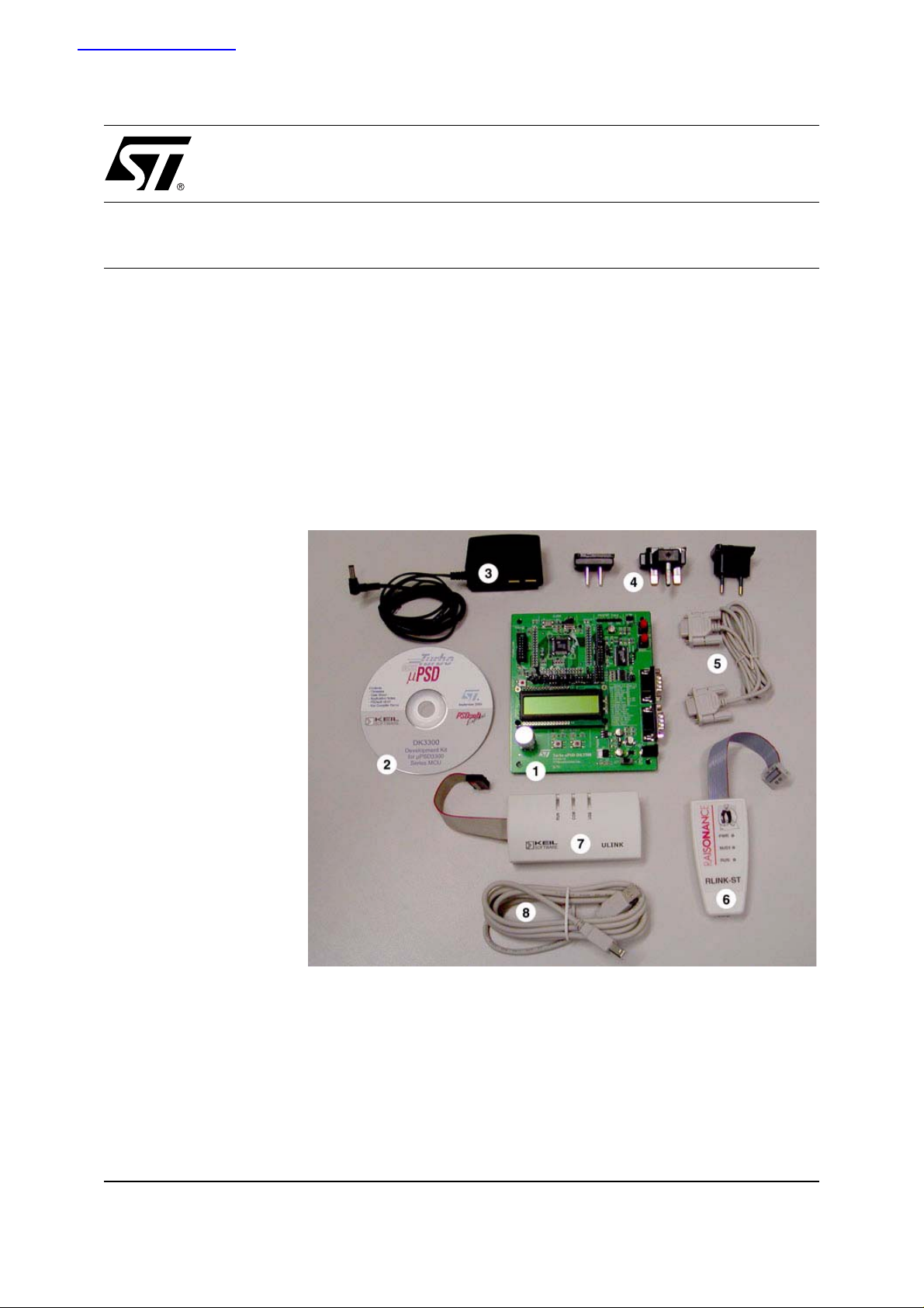
Figure 1. DK3300 Kit Contents
1. DK3300 Board
2. DK3300 CD
3. 110V/220V AC adapter
4. Plug adapters
5. RS232 Serial Cross-Over
Cable
6. USB R-LINK Adapter
7. USB ULink Adapter
8. USB Cable
9. Quick Start Flyer (not
shown)
1/11May 2004

UM0087 - USER MANUAL
TABLE OF CONTENTS
WELCOME TO THE DK3300 DESIGN KIT . . . . . . . . . . . . . . . . . . . . . . . . . . . . . . . . . . . . . . . . . . . . . . 1
Figure 1. DK3300 Kit Contents. . . . . . . . . . . . . . . . . . . . . . . . . . . . . . . . . . . . . . . . . . . . . . . . . . . . . 1
GETTING STARTED . . . . . . . . . . . . . . . . . . . . . . . . . . . . . . . . . . . . . . . . . . . . . . . . . . . . . . . . . . . . . . . . 3
Before you can use the uPSD . . . . . . . . . . . . . . . . . . . . . . . . . . . . . . . . . . . . . . . . . . . . . . . . . . . . 3
Step 1 - Install PSDsoft Express . . . . . . . . . . . . . . . . . . . . . . . . . . . . . . . . . . . . . . . . . . . . . . . . . . . . 3
Step 2 - Install Keil uVision2 . . . . . . . . . . . . . . . . . . . . . . . . . . . . . . . . . . . . . . . . . . . . . . . . . . . . . . . 3
Step 3 - Connecting the DK3300 Board . . . . . . . . . . . . . . . . . . . . . . . . . . . . . . . . . . . . . . . . . . . . . .4
Step 4 - Try Your DK3300 Board. . . . . . . . . . . . . . . . . . . . . . . . . . . . . . . . . . . . . . . . . . . . . . . . . . . . 4
Step 5 - Starting a Debugging Session . . . . . . . . . . . . . . . . . . . . . . . . . . . . . . . . . . . . . . . . . . . . . . . 4
Step 6 - Following the AN1763 Example. . . . . . . . . . . . . . . . . . . . . . . . . . . . . . . . . . . . . . . . . . . . . .4
DK3300 HARDWARE FEATURES. . . . . . . . . . . . . . . . . . . . . . . . . . . . . . . . . . . . . . . . . . . . . . . . . . . . .5
Figure 2. DK3300 Board Connections . . . . . . . . . . . . . . . . . . . . . . . . . . . . . . . . . . . . . . . . . . . . . . . 5
APPENDIX A.DK3300 JUMPERS . . . . . . . . . . . . . . . . . . . . . . . . . . . . . . . . . . . . . . . . . . . . . . . . . . . . .6
Table 1. DK3300 Jumpers. . . . . . . . . . . . . . . . . . . . . . . . . . . . . . . . . . . . . . . . . . . . . . . . . . . . . . . . 6
APPENDIX B.DK3300 SCHEMATICS . . . . . . . . . . . . . . . . . . . . . . . . . . . . . . . . . . . . . . . . . . . . . . . . . .7
Figure 3. MCU. . . . . . . . . . . . . . . . . . . . . . . . . . . . . . . . . . . . . . . . . . . . . . . . . . . . . . . . . . . . . . . . . .7
Figure 4. Peripheral . . . . . . . . . . . . . . . . . . . . . . . . . . . . . . . . . . . . . . . . . . . . . . . . . . . . . . . . . . . . . 8
Figure 5. Input/Output. . . . . . . . . . . . . . . . . . . . . . . . . . . . . . . . . . . . . . . . . . . . . . . . . . . . . . . . . . . . 9
REVISION HISTORY . . . . . . . . . . . . . . . . . . . . . . . . . . . . . . . . . . . . . . . . . . . . . . . . . . . . . . . . . . . . . . . 10
Table 2. Document Revision History. . . . . . . . . . . . . . . . . . . . . . . . . . . . . . . . . . . . . . . . . . . . . . . 10
2/11

UM0087 - USER MANUAL
GETTING STARTE D
Please insert the CD that comes with the Kit and print the following documents. These documents will help
you become familiar with the CD contents, the DK3300 Users Guide and an Application Note that will walk
you through a design example.
■ Read me text file (Readme.txt)
■ DK3300 Users Guide (UM0087.PDF)
■ AN1763 Example Design (AN1763.PDF)
■ Any errata file that may exist (*errata*.PDF)
Before you can use the uPSD
You will need to install some software on your PC system before you can program the DK3300. This includes PSDSoft Express and the Keil uVision Integrated Development Environment. Please follow the following steps to get started using the DK3300:
Step 1 - Install PSDsoft Express. Install the latest version of P SDsoft Express (from the Raisonance
CD).
Note: PSDSoft Express is required to configure the µ PSD device. Please che ck the ST Websi te for the
Latest PSDSoft version: www.st.com/micropsd
If you already have PSDSoft Express installed, then please install the update file by first unzipping the file
called Update_ExpressXXX.zip. This update file will automatically update your version of PSDSoft to support the Turbo µPSD3300.
If you do not have PSDSoft Express installed, then please install it by first unzipping the file called InstallExpressXXX.zip. This will install the s oftware needed to configure and optionally program t he Flash
inside the µPSD3300 product.
Step 2 - Install K e il uVisi on2. Install the latest version of Keil uVision2 Integrated Development Environment (ver 2.39 or greater). or the latest version of Raisonance’s Ride Environment.
Note: The Keil IDE or Raisonance IDE is required in order to make use of the JTAG debug f eat ure builtinto the µPSD3300. Please check the Keil website for the latest version: www.keil.com, or Raisonance
website: www.raisonance.com
If you already have uVision2 Integrated Development Environment from Keil Software Inc., and your Keil
software maintenance period has not expired, just update your uVision2 by double-clicking the file
UP51XXXX.exe located in the Keil directory on the CD.
If you do not have uVision2 Integrated Development Environment, you should install the trial version from
Keil in order to com pile t he ex amp le application des cribed in AN1763. To insta ll the trial version doubleclick the file EK51XXXX.exe located in the Keil directory on the CD.
3/11

UM0087 - USER MANUAL
Step 3 - Connecting the DK3300 Board. Connect the Cables to the DK3300 board (see Figure
2., page 5) by connecting the following cables from the DK330 0 board to your PC system.
1. Connect the AC adapter to the DK3300 board. The DK3300 AC adapter w ill wor k o n eithe r 110V or
220V, and contains several different plug adapters to fit popular European AC outlets. Please set up
your AC adapter to fit your AC plug type and plug in the AC adapter. Then plug the small power plug
into the DK3300 9V DC input.
2. Connect the R-LINK adapter to a USB port on your PC system by using the supplied USB cable.
3. Next, connect the small ribbon cable on the R-LINK adapter to the 14 pin JTAG connector on the
DK3300 board.
4. Start the PSDsoft application on your PC.
5. Make sure that you have selected R-LINK in the PSDsoft environment.
6. Test the R-LINK connection to ensure that PSDsoft and the R-LINK cable is communicating with your
DK3300 board.
7. Follow the Design Guide to program the desired design/demo in the uPSD using R-LINK and JTAG
port.
8. Verify that the correct application or demo is installed by viewing the LCD.
Note: The DK3300 may come with a pre-programmed demo described in AN1763.
9. Refer to the Design Guide and application notes for more details.
Step 4 - Try Your DK3300 Board. Your DK3300 board comes pre-programmed with the ADC demo application that is discussed in AN1763. To test your DK3300 board, you should have the AC adapter power
plugged in and connected to the 9V DC input on the DK3300 board.
Once you hav e confirmed your c onnections physically, turn the DK330 0 board on. Yo u should see t he
DK3300 AC demo running in the LCD window. If you do not see it running, please verify that you have
power by verifying the red power LED is on.
Note: Use the R-LINK adapter in conjunction with PSDsoft and Design guide to flash the other demos in
the DK3300 Kit to configure/reconfigure the uPSD device and then switch to ULink adapter to debug and
re-program the Flash as needed.
Step 5 - Starting a Debugging Session. To continue with the Raisonance debugging suite, leave the RLINK connected, otherwise for starting the Keil Tool chain, swap the R-LINK adapter for the ULink adapter.
The ULink/R-LINK adapters provided with DK3300 kit are used to debug the µPSD3300 with the built-in
JTAG debugger. It can optionally program the Flash in the µPSD3300 as well. This ULink/R-LINK adapter
plugs into the SAME 14-pin JTAG connector. Follow the IDE environment and the associated user’s guide
for debugging the codes.
Step 6 - Following the AN1763 Example. Read a nd follow the examp le in applica tion note A N1763 on
the CD.
This Application Note will guide you through a design cycle of the ADC demo to help you fam iliari ze yourself with PSDSoft Express (used to configure and program the uPSD device) and Keil’s uVision2 (used to
compose, compile, and debug firmware, as well as understand the architecture of the uPSD device).
4/11
UM0087 - USER MANUAL
DK3300 HARDWARE FEATURES
The uPSD3300 has many different IP features and the DK3300 board has a variety of hardware capabilities built into the demo board itself. Some hardware on the DK3300 board is provided to enable exploration by the customer and for future demo application software. Over time additional demo applications will
be added, so please check the ST website below for the latest demo applications. Some of the DK3300
board hardware features include (see Figure 2):
2
■ I
C Real Time Clock by ST with built in Crystal and Tamper Detect Logic
■ Tamper Detect switches connected to the ST RTC
■ Dual RS232 connectors driven by ST RS232 level shifter
■ SPI interface EEPR O M
■ IrDA Transceiver
■ Two input switches and two output LED’s
■ Rotary encoder with select switch
■ 2 Line by 16 Character LCD
Please check the ST uPSD website at www.st.com/micropsd for the latest updates to PSDSoft Express
and Demo Applications for the DK3300 kit.
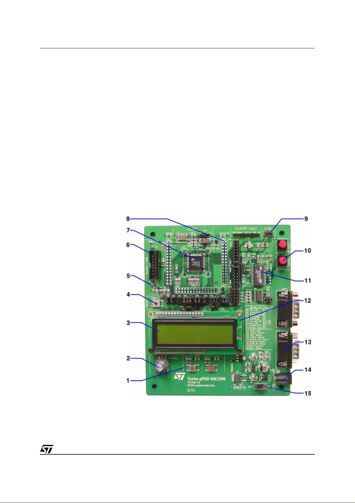
Figure 2. DK3300 Board Connections
1. Switches and LEDs
2. Rotary Encoder
3. LCD Display
4. Reset Switch
5. JTAG LED
6. 14-pin JTAG Connector
7. uPSD33XX
8. Expansion Connectors
9. IrDA Transceiver
10. Tamper Detect Switches
11. Real-Time Clock
12. EEPROM & Battery under
LCD
13. RS232 Connectors
14. 9VDC Power Input
15. On-Off Switch and Power
LED
5/11

UM0087 - USER MANUAL
APPENDIX A. DK3300 JUMPERS
Verify JP0, JP1, JP3, JP13, JP14, and JP 15 for the ADC dem o. Se e DK3300 SCHE MAT ICS, page 7 for
more information regarding the jumpers.
Table 1. DK3300 Jumpers
Jumper
No.
JP0 LCD Enable/Disable Normally closed to enable LCD
JP1
JP2 JTAG Debug I/O Pin Should be OPEN
JP3 LCD Contrast
JP4 Encoder Connection to PB
JP5 Switch / LED Connection to PB
JP6 MCU Clock Select Normally closed in position 1-2 for Oscillator. Position 2-3 for Crystal
JP7 Enable SPI Normally closed to enable SPI EEPROM
Description Comments
ADC V
Input Normally closed to set V
REF
Normally closed in position 2-3
Position 1-2 used for PWM control
Normally all 3 positions are closed to enable the encoder connection to
port B
Normally both positions are closed to enable the SW/LED connection to
port B
REF
= 3.3V
JP8 Reset Input Select
JP9 UART1 Select
JP10
JP11
JP12 Interrupt Select for MCU
JP13 PWM Channel Select
JP14 ADC Channel Select
JP15 PWM RC Constant Selects PWM RC constant. Normally position 1-2 (1ms) is closed.
JP16 N/A Not selectable – fixed at 3.3V
JP17
Used to connect UART0 and
Enable I
uPSD V
UART1 in loop back mode
2
C Normally both positions closed to enable I2C access to RTC chip.
STANDBY
Input
Normally closed in position 1-2 for reset switch input. Position 2-3 for RTC
reset.
Normally closed in position 1-3 and 2-4 to select the RS232 connector 1.
Else can be se to position 3-5 and 4-6 to select the Urdu transceiver to be
connected to UART1.
Normally open. Used to enable backup power to uPSD if needed.
Used to map various Interrupt sources to the MCU. Normally open (see
DK3300 SCHEMATICS, page 7).
Selects what PWM channel connects the RC circuit on the board.
Normally PWM0 is connected via position 1-2 closed.
Selects what ADC channel connects the RC circuit on the board. Normally
ADC7 is connected via position 15-16 closed.
Normally open. Can be connected positions 1-2 and 3-4 for loop back.
6/11
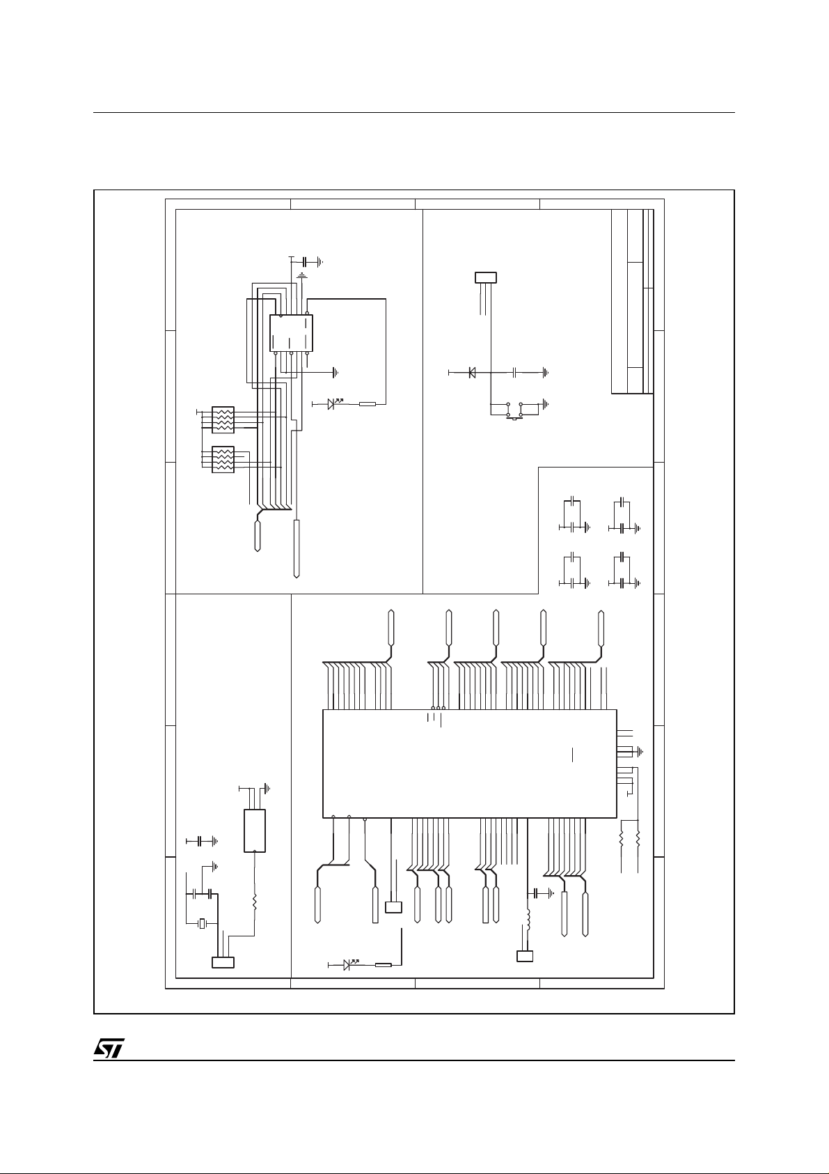
APPENDIX B. DK3300 SCHEM ATI CS
Figure 3. MCU
D
CC
C5
104P
FlashLINK
CPU_TMS
CPU_TCK
CPU_TSTA
CPU_JTAG
9
11
7
13
TCK
TDO
TMS
GND
GND
TERR
8
14
10
12
JTAG_CTRL
CPU_TERR
CPU_TDI
CPU_TDO
V
3
5
CC
TDI
V
TSTAT
RST
4
6
3.3V_RST
1
GND
CNTL
2
V
JEN
TRST
CC
6
54321
R2
10K
CC
V
4 5
3
6
2
7
1
8
R1
10K
4 5
3
6
2
7
1
8
RC_RST
C
D1
JEN
R4
470
B
123
JP8
3.3V_RST
RESET
RC_RST
D3
1N4148
CC
V
C4
105P
FlashLINK JTAG for 3300 Programming/Debugging
RESET
SWITCH
PUSH-BUTTON
UM0087 - USER MANUAL
A
Revision
Reset Circuit
Number
C:\Documents and Settings\bo kang.ST
MCU
SizeBDate: 4-August-2003 Sheet 2 of 4
File:
Title
4 3
1 2
C12
3.3V
C9
C11
104P
104P
103P
3.3V
C10
C7
C16
103P
103P
103P
3.3V low active RESET
MCU
Clock
41 CPU_AD4
37 CPU_AD1
38 CPU_AD2
39 CPU_AD3
36 CPU_AD0
P0.1/AD1
P0.2/AD2
P0.3/AD3
P0.0/AD0
CC
V
1
2
4
CC
OE
V
C13
104P
CC
V
X2
C18
20pf
C17
20pf
40MHz
X2
GND
OSC_OUT
X1
40MHz
3
R12
200
U3
DK3300
CPU_CLOCK
X148X2
X1
49
X2
47 CPU_AD7
45 CPU_AD6
43 CPU_AD5
P0.4/AD4
P0.5/AD5
P0.6/AD6
P0.7/AD7
RESET_IN
68
3.3V_RST
AD[0.. 11]
51 CPU_AD8
53 CPU_AD9
55 CPU_AD10
57 CPU_AD11
P2.1/A9
P2.2/A10
P2.3/A11
P2.0/A8
DEBUG
8
CPU_DEBUG
1
JP2
3.3V Reset
JTAG_CNTRL
2
X1
D2
123
JP6
D
DEBUG
CC
V
C
R7
470
JTAG_CNTRL
Reset
JTAG (FlashLINK)
62 CPU_WR
4 CPU_ALE
63 CPU_PSEN
65 CPU_RD
CTRL0/RD
CTRL0/WR
CTRL2/PSEN
CSDA/P3.6
2
RXD/P3.0
TXD/P3.1
EXINT0/GATE0/P3.2
EXINT1/GATE1/P3.3
T0/P3.4
T1/P3.5
I
44
46
77
79240
42
75
CPU_U1RXD
CPU_U1TXD
CPU_INT0
CPU_INT1
CPU_P3.4
CPU_P3.5
CPU_I2CSDA
CPU_I2CSCL
CPU_P3
CPU_CMM
Control Bus
35 CPU_PA0
34 CPU_PA1
PA0
PA1
ALE(PD0)
CSCL/P3.7
2
I
CPU_I2C
32 CPU_PA2
28 CPU_PA3
26 CPU_PA4
24 CPU_PA5
PA2
PA3
PA4
PA5
.
ADC0/T2/P1.0
ADC1/T2x/P1.1
52
54565859606164
CPU_ADC0
CPU_ADC1
CPU_ADC_IN
B
PA[0.. 7]
22 CPU_PA6
21 CPU_PA7
80 CPU_PB0
78 CPU_PB1
76 CPU_PB2
PA6
PA7
PB0
PB1
ADC2/RXD2/P1.2
ADC3/TXD2/P1.3
ADC4/SPISCLK/P1.4
ADC5/SPIRXD/P1.5
ADC6/SPITXD/P1.6
CPU_ADC4
CPU_ADC5
CPU_ADC6
CPU_ADC7
CPU_U2RXD
CPU_U2TXD
CPU_UART2
JP1
74 CPU_PB3
73 CPU_PB4
71 CPU_PB5
PB2
PB3
PB4
REF
ADC7/SPISEL/P1.7
V
70
REF
V
L1
3.3V
1
2
PB[0.. 7]
67 CPU_PB6
66 CPU_PB7
PB5
PB6
PB7
T2/TCM0/P4.0
33
CPU_PWM0
C8
104P
100µH
C15
VC1
20 CPU_TMS
16 CPU_TCK
15 CPU_PC2
14 CPU_TSTA
9 CPU_TERR
/PC4
/PC2
TCK/PC1
TMS/PC0
STBY
V
TSTAT/RDY/PC3
TERR/V
T2x/TCM1/P4.1
RXD2/TCM2/P4.2
TXD2/PCA0/P4.3
SPISCLK/TCM3/P4.4
SPIRXD/TCM4/P4.5
CPU_PWM1
CPU_PWM2
CPU_PCA0CLK
CPU_SPI_CLK
CPU_SPI_RXD
CPU_PWM_OUT
104P
7 CPU_TDI
BATON
CPU_SPI_TXD
VC1
CPU_JTAG
6 CPU_TDO
5 CPU_PC7
3 CPU_PD1
1 CPU_PD2v
PC7
PD1
PD2
N.C.
TDI/PC5
N.C.
TDO/PC6
GND
GND
GND
DD
V
DD
V
CC
V
CC
V
SPITXD/TCM5/P4.6
SPISEL/PCA1/P4.7
18192325302731
CPU_SPI_SEL
CPU_SPI_BUS
A
C14
104P
17
11
69
29
13
50
12
10
72
3.3V
VC1
R16
0R80
5V
3.3V
1 2 3 4 56
AI09611
7/11

UM0087 - USER MANUAL
Figure 4. Peripheral
D
1
2
JP11
6
OUT
M41ST87_V
CPU_PC2
OUT
TPCLR
ECON
M41ST87_V
25
18
R29
0
3.3V
4K7
4K7
3.3V or 5V
15
28
0
C33
GND
4 5
3
2
1
104pF
RESET
U7
CLR
OUT
V
TP
BAT
V
CC
V
SDA17SCL22EX27WDI9RST INT110RST INT211PFI1
F32K
I2CSDA
I2CSCL
1
CON6
54321
6
7
8
CC
V
BATTERY
Battery Socket
R28
5V
R22
R24
M41ST87_IRQ
M41ST87_SQW
26
IRQ
SQW
ECON
V
2
M41ST87_PFO1
M41ST87_PFO2
RESET
7
12
19168
RST
PFO1
23
CC
1
2
CON5
PFO2
13
R18
1 2
JP13
CPU_PWM0
CPU_PWM1
A
JP15
10K
8
109
3 4
5 6127
CPU_PWM2
CPU_SPI_CLK
CPU_SPI_RXD
Revision
Number
C:\Documents and Settings\bo kang.ST
Peripheral
SizeBDate: 4-August-2003 Sheet 3 of 4
File:
Title
C25
104pF
C24
105pF
11
CPU_SPI_TXD
CPU_PWM
12
13
11
M41ST87_PFO
M41ST87_SQW
SENSOR2
GND
B
15
14
CPU_PB1
GND
1 2163
JP14
CPU_ADC0
4
6
8
5
7
CPU_ADC1
CPU_ADC4
CPU_U2RXD
CPU_U2TXD
7101ADC
LCD_VL
14
12
109
13
11
CPU_ADC5
CPU_ADC6
CPU_ADC7
15
7101UART2
C
CSCL
CSDA
2
2
I
I
1 2
3 4
JP10
CPU_I2CSCL
CPU_I2CSDA
123
4
JP18
F32k
GND
ECON
TPCLR
CPU_INT0
R27
R25
CPU_INT1
1
3254
687910
JP12
2
M41ST87_IRQ
M41ST87_PFO
1k2
1k2
F32k
21
F32k
M41ST87
SS
V
14
PFI2
TP1IN
TP2IN
20
24
SENSOR1
R23
6k8
R26
R21
10K
V_UNREG
3k6
5V
CON4
OUT
M41ST87_V
123
CON3
PWM, ADC
I2C Interface Circuit with Battery
C6
104P
CC
V
2
SPI Interface Circuit
LCD Interface Circuit
CPU_SPI_RXD
3.3V
GND
CC
CPU_SPI_CLK
CPU_SPI_TXD
V
8
6
7
D5C
CC
V
HOLD
SS
W3V
S
Q
U4
M95080W
4
1
2
R15
10K
CC
V
CC
CPU_SPI_RXD
V
SPI_SEL
CPU_SPI_SEL
2
JP7
C19
1
104P
CC
V
D
7
8
Q
D1C
U10
2
CPU_SPI_TXD
CPU_SPI_CLK
3.3V
SS
V
3.3V
6
5
CC
V
RESET
4
3
3.3V_RST
SPI_SEL
C35
104P
W
S
48PE16
C
5V
D07D18D29D310D411D512D613D714VL3RS4R/W5E
LCD
PA[0.. 7]
CPU_PA0
CPU_PA1
CPU_PA2
CPU_PA3
CPU_PA4
CPU_PA5
LCD Module Only Operates on 5V
R11
1K
R10
4K7
5V
LCD_EN
CPU_PB7
1
2
JP0
B
CPU_PA6
CPU_PA7
JP3
R0
4K7
CPU_PB6
CPU_PB5
123
GND
LCD Module
6
LCD_EN
1
PB[5.. 7]
5V
5V
8
7
5
6
CC
IP-B
V
IP_B
OP-B
IP-A2IP_A3GND
OP-A
LM358
U2
1
4
LCD_VL
C3
104pF
1 2 3 4 56
A
AI09612
8/11

Figure 5. Input/Output
UM0087 - USER MANUAL
D
C
B
A
UART2
162738495
UART1
162738495
6
RS232_RXD0
RS232_TXD0
C21
334pF
TXD1
RS232_TXD0
14
C2+
OUT
T1
IN
T1
11
CPU_U1TXD
VREF
CPU_DEBUG
CPU_ADDR_DATA
CPU_AD7
CPU_AD6
CPU_AD5
CPU_PD2
CPU_PD1
CPU_PC7
RXD1
RS232_RXD0
7
8
13
IN
OUT
R1
T2
OUT
IN
R1
T2
9
12
10
CPU_U1RXD
CPU_A11
GND
CPU_A10
CPU_A9
CPU_A8
CPU_AD4
CPU_AD3
CPU_AD2
CPU_AD1
CPU_AD0
CPU_TDO
CPU_TDI
CPU_TERR
CPU_TSTAT
CPU_PC2
IN
R2
OUT
R2
CPU_U1RXD
CPU_U1TXD
CPU_P3
CPU_PWM0
CPU_PWM1
CPU_P4
CPU_TCK
CPU_TMS
CC
V
5
16
4
CC
C2–
V
C1+1C1–
V+
U8
54321
CC
V
CON1
CON3
CON2
3
2
C23
334pF
C22
334pF
CPU_COMM
30
CPU_RD
CPU_PSEN
CPU_WR
CPU_ALE
3.3V_RST
GND
5V
5V
Reset
1234567891011121314151617181920212223242526272829
CPU_ADC0
CPU_ADC1
CPU_U2RXD
CPU_U2TXD
CPU_ADC4
CPU_ADC5
CPU_ADC6
CPU_ADC7
CPU_P1 CPU_CTRL
1234567891011121314151617181920212223242526272829
CPU_PB7
CPU_PB6
CPU_PB5
CPU_PB4
CPU_PB3
CPU_PB2
CPU_PB1
CPU_PB0
D
TXD1
RXD1
15
GND
V–
ST3232
6
RS232 Interface Circuit
C20
334pF
1
CPU_INT0
CPU_INT1
CPU_P3.4
CPU_P3.5
CPU_I2CSDA
CPU_I2CSCL
CPU_PWM2
CPU_PCA0CLK
CPU_SPI_CLK
CPU_SPI_RXD
CPU_SPI_TXD
CPU_SPI_SEL
CPU_PA7
CPU_PA6
CPU_PA5
CPU_PA4
CC
V
U9
TFDU4203
4
IrDA Interface Circuit (disable shutdown)
364
2
5
CPU_U2RXD
CPU_U2TXD
1234567891011121314151617181920212223242526272829
CON30
Connector
X2
VCC
VCC
GND
30
CON30
3.3V
CC
V
30
CON30
CPU_PA3
CPU_PA2
CPU_PA1
CPU_PA0
C
R19
5
CC
RXD
V
TXD
2
3
7
R20
C32
104pF
CC
V
TXD1
RXD1
12
34
JP17
RS232_TXD0
RS232_RXD0
Encoder, Button, & LED
R9
4k7
6
7
CC
V
8
10
C34
C31
GND1GND
4.7µF
104pF
SD
6
8
0
ENCODER
4 5
3
2
1
445
3
JP4
GND5GND
RS232, IrDA
5
11223
*
10K
R5
R3 10K
123456
CPU_PB2
CPU_PB3
CPU_PB4
B
5V
3
OUT
V
IN
V
U6
78M05-5V
1
UNREG
V
D5
1
J1
Power Supply
CC
C1
103P
V
C2
103P
D4
POWER
C26
104pF
GND
2
220µF
C30
1N4004
SWITCH
LED_TWO
R14
LED_ONE
1K5
R13
R17
1K
3.3V
2
OUT
V
IN
V
U5
LD1117-3.3V
3
5V
JP16
KEY2 SW
12
43
KEY1 SW
12
43
JP5
1K5
C28
10µF
C27
104pF
GND
1
C29
10µF
123
3.3V5VVCC
PUSH-BUTTON
PUSH-BUTTON
12
34
CPU_PD2
CPU_PD1
A
Revision
Number
C:\Documents and Settings\bo kang.ST
Input/Output
SizeBDate: 4-August-2003 Sheet 4 of 4
File:
Title
1 2 3 4 56
AI09613
9/11

UM0087 - USER MANUAL
REVISION HISTORY
Table 2. Document Revision History
Date Version Revision Details
May 7, 2004 1.0 First Issue
10/11

UM0087 - USER MANUAL
If
this d
you have any questions or suggestions concerning the matters raised in
ocument, please send them to
the following electronic mail addresses:
ask.memory@st.com (for general enquiries)
Please remember to include your name, company, location, telephone number and fax number.
Information furnished is believed to be accurate and reliable. However, STMicroelectronics a ssumes no responsibility fo r the c onsequences
of use of such information nor for any infringement of patents or other rights of third parties which may result from its use. No license is granted
by implication or otherwise under any patent or patent rights of STMicroelectronics. Specifications mentioned in this publication are subject
to change without notice. This publication supersedes and replaces all information previously supplied. STMicroelectronics products are not
authori zed for use as criti cal components in life support devices or systems without ex press written approval of ST M i croelectronics.
The ST logo is a registered tra dem ark of STMicroelectronics.
All other na m es are the property of their re spective owner s.
© 2004 STMi croelectroni cs - All rights res erved
Australi a - B elgium - Brazi l - Canada - Chin a - Czech Republ i c - Finland - Fra nce - Germany -
Hong Kong - India - Israel - It al y - Japan - Malaysi a - Malta - Morocco - Singapor e -
STMicroelectroni cs GROUP OF COMPANIES
Spain - Sweden - Switzerland - United Kingdom - United States
www.st.com
11/11
 Loading...