

ST ULQ2801A, ULQ2804A, ULQ2805A, ULQ2802A, ULQ2803A User Manual

®
EIGHT DARLINGTONS PER PA CKAGE
.
EXTENDED TEMPERATURE RANGE
.
(– 40 to 105
.
OUTPUT CURRENT TO 500m A
.
OUTPUT VOLTAGE TO 50V
.
INTEGRAL SUPPRESSION DIODES
.
VERSIONS FOR ALL POPULAR LOGIC FAMILIES
.
OUTPUT CAN BE PARALLELED
.
INPUTS PINNED OPPOSITE OUTPUTS TO
SIMPLIFY BOARD LAYOUT
°C)
ULQ2801A
ULQ2802A - UL Q2803A
ULQ2804A - UL Q2805A
EIGHT DARLINGTON ARRA YS
DIP18
(Plastic Package)
DESCRIPTION
The ULQ2 801A-U LQ2805A each co ntain eight darlington transistors with common emitters and integral suppression diodes for inductive loads. Each
darlington features a peak load current rating of
600mA (500mA continuous) and can withstand at
least 50V i n the off state. Outpu ts may be parall eled
for higher c ur re nt cap abi lit y .
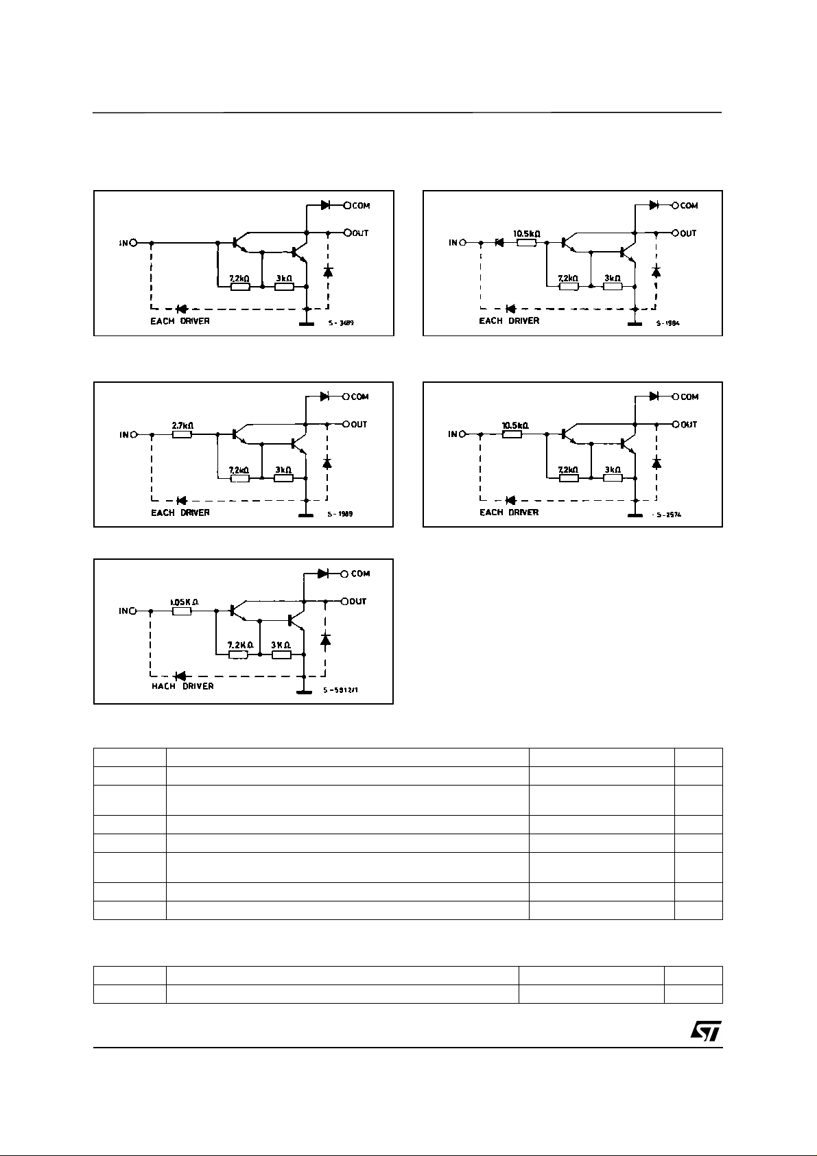
Five ver s ions are available t o s im p lif y in t erfa ci ng to
standard lo gic f amil ies : the UL Q2801A is desi gned
for gene ra l p ur pos e applicatio ns w it h a c ur re nt l im it
resistor ; the ULQ2802A has a 10.5k Ω input res istor
and zener for 14 -25V PMOS ; the ULQ280 3A has a
2.7kΩ input resistor for 5V TTL and CMOS ; the
ULQ2804A has a 10.5kΩ input resistor for 6-15V
CMOS and the ULQ2805A is designed to sink a
minimum of 350mA for standard and Schottky TTL
where higher output curren t i s required.
All types are supplied in a 18-lead plastic DIP with
a copper le ad f ra me and feature the convenient input-oppo si te-o ut put pinout to simpli fy bo ar d lay out.
Septembe r 200 3
PIN CONNECTION
(top view)
1/8
ULQ2801A - ULQ2802A - ULQ2803A - ULQ2804A - ULQ2805A
SCHEMATIC DIAGRAM AND ORDER CODES
For ULQ28 01A ( eac h dr iv er f or PM O S - CMO S ) For ULQ2802A (eac h dr iv er for 14- 15 V PMOS)
For ULQ2 803A (each drive r for 5 V , TTL/CMOS) For ULQ2804A (each driv er for 6-15 V
CMOS/PMOS
For ULQ2 805A (each drive r for high out TTL)
ABSOLUTE MAXIMUM RATIN GS
Symbol Parameter Value Unit
V
o
V
I
C
I
B
P
tot
T
amb
T
stg
Output Voltage 50 V
Input Voltage for ULQ2802A, 2803A, 2804A
i
for ULQ2805A
30
15
Continuous Collector Current 500 mA
Continuous Base Current 25 mA
Power Dissipation (one Darlington pair)
(total package)
1.0
2.25
Operating Ambient Temperature Range – 40 to 105 °C
Storage Temperature Range – 55 to 150 °C
V
V
W
W
THERMAL DATA
Symbol Parameter Value Unit
2/8
R
th j-amb
Thermal Resistance Junction-ambient Max. 55 °C/W
ULQ2801A - ULQ2802A - ULQ2803A - ULQ2804A - ULQ2805A
= –40 to 105oC, unless otherwise specified)
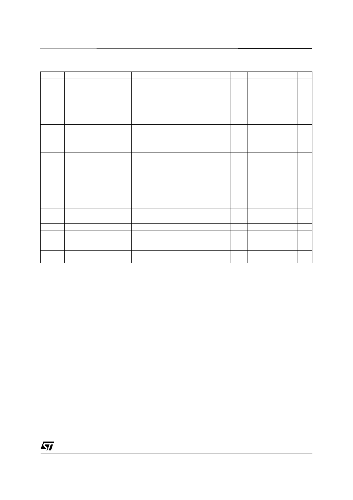
ELECTRICAL CHARACTERISTICS
Symbol Parameter Test Conditions Min. Typ. Max. Unit Fig.
I
V
CE (sat)
I
I
V
h
t
t
(*) Guaranteed by design
Output Leakage Current VCE = 50V
CEX
Collector-emitter
Saturation Voltage
Input Current for ULQ2802A Vi = 17V
i(on)
Input Current TJ = 105°C, IC = 500µA5065µA4
i(off)
Input Voltage for ULQ2802A VCE = 2V, Ic = 300mA
i(on)
DC Forward Current Gain for ULQ2802A VCE = 2V, Ic = 350mA 1000 – 2
FE
C
Input Capacitance 15 25 (*) pF –
i
Turn-on Delay Time 0.5 Vi to 0.5 V
PLH
Turn-off Delay Time 0.5 Vi to 0.5 V
PHL
Clamp Diode Leakage
I
R
Current
Clamp Diode Forward
V
F
Voltage
(T
j
50
µA
TJ = 105°C, VCE = 50V
= 105°C
T
J
for ULQ2802A VCE = 50V, Vi = 6V
for ULQ2804A VCE = 50V, Vi = 1V
IC = 100mA, IB = 250µA
IC = 200mA, IB = 350µA
= 350mA, IB = 500µA
I
C
for ULQ2803A Vi = 3.85V
for ULQ2804A V
= 5V
i
Vi = 12V
for ULQ2805A Vi = 3V
for ULQ2803A V
= 2V, Ic = 200mA
CE
VCE = 2V, Ic = 250mA
VCE = 2V, Ic = 300mA
for ULQ2804A V
= 2V, Ic = 125mA
CE
VCE = 2V, Ic = 200mA
VCE = 2V, Ic = 275mA
= 2V, Ic = 350mA
V
for ULQ2805A VCE = 2V, Ic = 350mA
CE
o
o
VR = 50V
= 105°C, VR = 50V
T
J
100
µA
500
µA
500
µA
0.9
1.1
1.3
0.82
0.93
0.35
1
1.5
1.1
1.3
1.6
1.25
1.35
0.5
1.45
2.4
13
2.4
2.7
2.4
V
V
V
mA
mA
mA
mA
mA
V
V
V
3
V
5
V
6
V
7
V
8
V
V
0.25 1 (*) µs–
0.25 1 (*) µs–
50
µAµA6
100
IF = 350mA 1.7 2 V 7
1a
1a
1b
1b
2
3
5
3/8
 Loading...