Datasheet ULQ2805A, ULQ2804A, ULQ2803A, ULQ2802A, ULQ2801A Datasheet (SGS Thomson Microelectronics)

.EIGHT DARLINGTONSPER PACKAGE
.EXTENDEDTEMPERATURE RANGE
(– 40 to 105°C)
.OUTPUTCURRENT TO 500mA
.OUTPUTVOLTAGETO50V
.INTEGRALSUPPRESSIONDIODES
.VERSIONSFOR ALL POPULARLOGICFAMI-
LIES
.OUTPUTCANBE PARALLELED
.INPUTS PINNED OPPOSITE OUTPUTS TO
SIMPLIFYBOARDLAYOUT
ULQ 2801A
ULQ2802A - ULQ2803A
ULQ2804A - ULQ2805A
EIGHTDARLINGTON ARRAYS
DIP18
(PlasticPackage)
DESCRIP TION
TheULQ2801A-ULQ2805Aeachcontaineightdarlington transistorswith common emitters and integral suppression diodes for inductive loads. Each
darlington features a peak load current rating of
600mA (500mA continuous)and can withstand at
least50Vin theoffstate.Outputsmaybeparalleled
for highercurrent capability.
Fiveversionsare availableto simplify interfacingto
standardlogic families: theULQ2801Ais designed
for generalpurposeapplicationswitha current limit
resistor; theULQ2802Ahasa 10.5kΩinputresistor
and zenerfor14-25VPMOS; theULQ2803Ahasa
2.7kΩ input resistor for 5V TTL and CMOS ; the
ULQ2804Ahas a 10.5kΩ input resistor for 6-15V
CMOS and the ULQ2805A is designed to sink a
minimumof 350mAfor standardand SchottkyTTL
wherehigheroutput currentis required.
Alltypes are suppliedin a 18-leadplastic DIP with
a copper lead frameand feature the convenientinput-opposite-outputpinout to simplifyboard layout.
April1993
PIN CONNECTI ON (top view)
1/8

ULQ2801A - ULQ2802A - ULQ2803A - ULQ2804A - ULQ2805A
SCHEMATIC DIA G RAM AND ORDER CODES
ForULQ2801A(eachdriver forPMOS-CMOS)For ULQ2802A(each driver for14-15 V PMOS)
For ULQ2803A(eachdriver for 5V, TTL/CMOS) For ULQ2804A (each driver for 6-15 V
CMOS/PMOS
For ULQ2805A(eachdriver for highout TTL)
ABSOLUTE MAXIMUM RATINGS
Symbol Parameter Value Unit
V
o
V
I
C
I
B
P
tot
T
amb
T
stg
Output Voltage 50 V
Input Voltage for ULQ2802A, 2803A, 2804A
i
for ULQ2805A
30
15
Continuous Collector Current 500 mA
Continuous Base Current 25 mA
Power Dissipation (one Darlington pair)
(total package)
1.0
2.25
Operating Ambient Temperature Range – 40 to 105 °C
Storage Temperature Range – 55 to 150 °C
V
V
W
W
THERMAL DATA
Symbol Parameter Value Unit
Thermal Resistance Junction-ambient Max. 55 °C/W
2/8
R
th j-amb

ULQ2801A - ULQ2802A - ULQ2803A - ULQ2804A - ULQ2805A
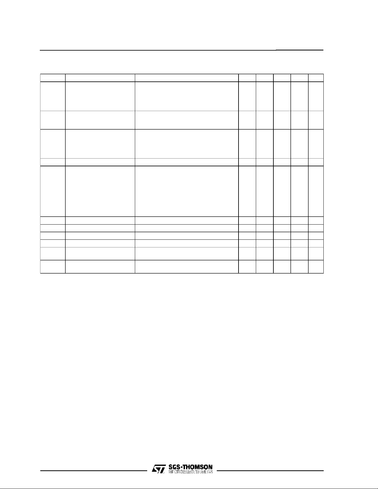
ELECTRICAL CHARACTERISTICS (Tj= –40 to 105oC, unless otherwise specified)
Symbol Parameter Test Conditions Min. Typ. Max. Unit Fig.
I
V
CE (sat)
I
I
V
h
t
t
(*) Guaranteed by desi gn
Output Leakage Current VCE= 50V
CEX
Collector-emitter
Saturation Voltage
Input Current for ULQ2802A Vi= 17V
i(on)
Input Current TJ= 105°C, IC= 500µA5065µA4
i(off)
Input Voltage for ULQ2802A VCE= 2V, Ic= 300mA
i(on)
DC Forward Current Gain for ULQ2802A VCE= 2V, Ic= 350mA 1000 – 2
FE
C
Input Capacitance 15 25 (*) pF –
i
Turn-on Delay Time 0.5 Vito 0.5 V
PLH
Turn-off Delay Time 0.5 Vito 0.5 V
PHL
I
Clamp Diode Leakage
R
Current
V
Clamp Diode Forward
F
Voltage
= 105°C, VCE= 50V
T
J
= 105°C
T
J
for ULQ2802A V
for ULQ2804A V
= 50V, Vi=6V
CE
= 50V, Vi=1V
CE
IC= 100mA, IB= 250µA
= 200mA, IB= 350µA
I
C
= 350mA, IB= 500µA
I
C
0.82
for ULQ2803A V
for ULQ2804A V
for ULQ2805A V
for ULQ2803A V
for ULQ2804A V
for ULQ2805A V
= 3.85V
i
=5V
i
= 12V
V
i
=3V
i
= 2V, Ic= 200mA
CE
= 2V, Ic= 250mA
V
CE
= 2V, Ic= 300mA
V
CE
= 2V, Ic= 125mA
CE
= 2V, Ic= 200mA
V
CE
= 2V, Ic= 275mA
V
CE
= 2V, Ic= 350mA
V
CE
= 2V, Ic= 350mA
CE
o
o
0.93
0.35
0.25 1 (*) µs–
0.25 1 (*) µs–
VR= 50V
= 105°C, VR= 50V
T
J
IF= 350mA 1.7 2 V 7
0.9
1.1
1.3
1
1.5
50
100
500
500
1.1
1.3
1.6
1.25
1.35
0.5
1.45
2.4
13
2.4
2.7
3
5
6
7
8
2.4
50
100µAµA
µA
µA
µA
µA
V
V
V
mA
mA
mA
mA
mA
V
V
V
V
V
V
V
V
V
1a
1a
1b
1b
2
3
5
6
3/8

ULQ2801A - ULQ2802A - ULQ2803A - ULQ2804A - ULQ2805A
TEST CIRCUITS
Figure 1a. Figure 1b.
Figure 2. Figure3.
Figure 4. Figure5.
Figure 6. Figure7.
4/8

ULQ2801A - ULQ2802A - ULQ2803A - ULQ2804A - ULQ2805A
Figure 8 : CollectorCurrent as a Functionof
SaturationVoltage.
Figure 10 : AllowableAveragePower Dissipation
as a Functionof Ambient Temperature.
Figure9 : CollectorCurrent as a Functionof
InputCurrent.
Figure11 : PeakCollector Current as a Function
ofDutyCycle.
Figure 12 : PeakCollectorCurrent asa Function
of Duty.
Figure13 : Input Currentasa Functionof Input
Voltage(forULQ2802A).
5/8

ULQ2801A - ULQ2802A - ULQ2803A - ULQ2804A - ULQ2805A
Figure 14 : InputCurrent as a Functionof Input
Voltage(forULQ2804A)
Figure 16 : InputCurrent as a Functionof Input
Voltage(forULQ2805A)
Figure15: InputCurrentasa Functionof Input
Voltage(for ULQ2803A)
6/8

ULQ2801A - ULQ2802A - ULQ2803A - ULQ2804A - ULQ2805A
DIP18 PACKAGE MECHANICAL DATA
DIM.
MIN. TYP. MAX. MIN. TYP. MAX.
a1 0.254 0.010
B 1.39 1.65 0.055 0.065
b 0.46 0.018
b1 0.25 0.010
D 23.24 0.915
E 8.5 0.335
e 2.54 0.100
e3 20.32 0.800
F 7.1 0.280
I 3.93 0.155
L 3.3 0.130
Z 1.27 1.59 0.050 0.063
mm inch
7/8

ULQ2801A - ULQ2802A - ULQ2803A - ULQ2804A - ULQ2805A
Information furnished is believed to be accurate and reliable. However, SGS-THOMSON Microelectronics assumes no responsibility for
the consequences of use of such information nor for any infringement of patents or other rights of third parties which may result from its
use. No license is granted by implication or otherwise under any patent or patent rights of SGS-THOMSON Microelectronics. Specifications mentioned in this publication are subject to change without notice. This publication supersedes and replaces all information previously supplied. SGS-THOMSON Microelectronics products are not authorized for use as critical components in life support devices or
systems without express written approval of SGS-THOMSON Microelectronics.
1994 SGS-THOMSON Microelectronics - All Rights Reserved
Australia - Brazil - France- Germany - Hong Kong - Italy - Japan - Korea - Malaysia - Malta - Morocco - The Netherlands - Singapore -
SGS-THOMSON Microelectronics GROUP OF COMPANIES
Spain - Sweden - Switzerland- Taiwan - Thaliand - United Kingdom - U.S.A.
8/8
 Loading...