

Page 1
UC2842B/3B/4B /5B
UC3842B/3B/4B /5B
March 1999
HIGH PERFORMANCE CURRENT MODE PWM CONTROLLER
.
TRIMMED OSCILLATOR FOR PRECISE FREQUENCY CONTROL
.
OSCILLATOR FREQUENCY GUARANTEED
AT 250kHz
.
CURRENT MODE OPERATION TO 500kHz
.
AUTOMATIC FEED FORWARD COMPENSATION
.
LATCHING PWM FOR CYCLE-BY-CYCLE
CURRENT LIMITING
.
INTERNALLY TRIMMED REFERENCE WITH
UNDERVOLTAGE LOCKOUT
.
HIGH CURRENT TOTEM POLE OUTPUT
.
UNDERVOLTAGE LOCKOUT WITH HYSTERESIS
.
LOW STAR T-UP AND O PERA TING CURR ENT
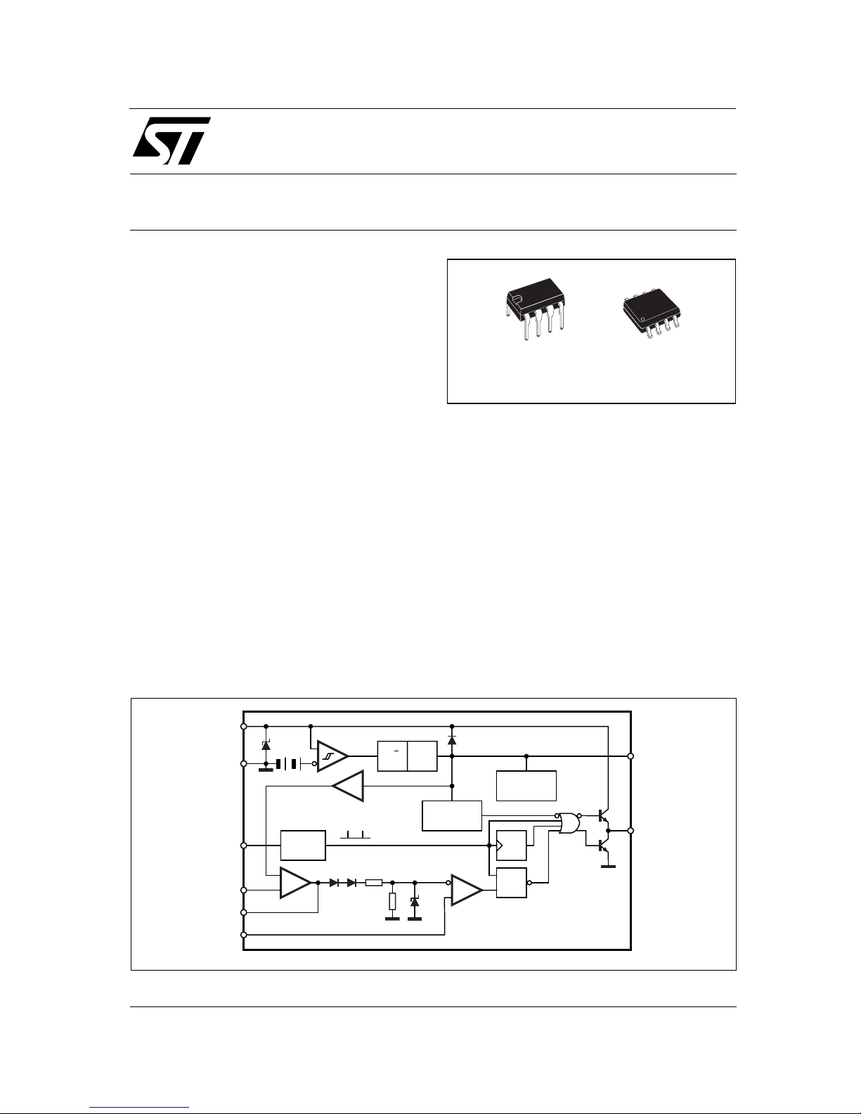
DESCRIPTION
The UC38 4xB family of control ICs provi des the necessary features to implement off-line or DC to DC
fixed freq uency c urrent mod e cont rol sch emes with
a minimal external parts count. Internally implemented cir cuits i nclude a trimmed os cil lator fo r precise DUTY CYCLE CONTROL under voltage lockout featuring start-up current les s than 0.5mA, a precision reference trimmed for accuracy at the error
amp input , logic to in sure la tched oper ation, a PW M
comparator wh ich also provides current limit control,
and a totem pole output stage designed to source
or sink high pe ak current. The output stage, su itable
for driving N-Channel MOSFETs, is low in the offstate.
Differences between members of this family are the
under-voltage lockout thresholds and maximum duty
cycle ranges. The UC3842B and UC3844B have
UVLO thresholds of 16V (on) and 10V (o ff), ideally
suited off-line applications The corresponding thresholds for the UC3843B and UC3845B are 8.5 V and 7.9
V. The UC3842B and UC3843B can operate to duty
cycles approaching 100%. A range of the zero to <
50 % is obtained by the UC3844B and UC3845B by
the addition of an internal toggle flip flop which blanks
the output off every other clock cycle.
BLOCK DIAGRAM (toggle flip flop used only in UC3844B and UC3845B)
UVLO
S/R
5V
REF
34V
INTERNAL
BIAS
VREF GOOD
LOGIC
2.50V
T
S
R
OSC
R1V
CURRENT
SENSE
COMPARATOR
2R
+
-
PWM
LATCH
7
5
4
2
1
3
8
6
ERROR AMP.
Vi
GROUND
RT/CT
VFB
COMP
CURRENT
SENSE
VREF
5V 50mA
OUTPUT
D95IN331
Minidip
®
SO8
UC3842B
1/15
Page 2
*
All voltages are with respe ct to pi n 5, al l currents are pos itive i nto t he spec i fied terminal.
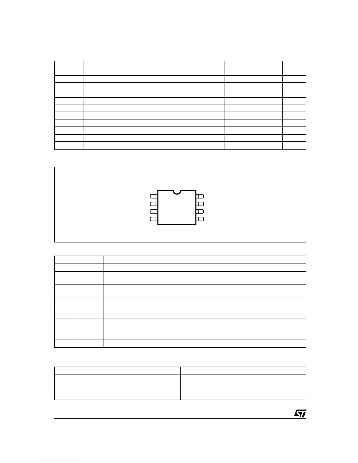
PIN CONNECTION (top view)
COMP
V
FB
I
SENSE
RT/C
T
GROUND
OUTPUT
Vi
V
REF
1
3
2
4
6
5
7
8
D95IN332
Minidi p/ SO 8
ORDERING NUMBERS
SO8 Minidip
UC2842BD1; UC3842BD1
UC2843BD1; UC3843BD1
UC2844BD1; UC3844BD1
UC2845BD1; UC3845BD1
UC2842BN; UC3842BN
UC2843BN; UC3843BN
UC2844BN; UC3844BN
UC2845BN; UC3845BN
ABSOLUTE MAXIMUM RATINGS
Symbol Parameter Value Unit
V
i
Supply Voltage (low impedance source) 30 V
V
i
Supply Voltage (Ii < 30mA) Self Limiting
I
O
Output Cur re nt
±
1
A
E
O
Output Energy (capacitive load) 5
µ
J
Analog Inputs (pins 2, 3) – 0.3 to 5.5 V
Error Amplifier Output Sink Current 10 mA
P
tot
Power Dissipation at T
amb
≤ 25 °C (Minidip)
1.25 W
P
tot
Power Dissipation at Tamb ≤ 25 °C (SO8)
800 mW
T
stg
Storage Temperature Range – 65 to 150
°
C
T
J
Junction Operating Temperature – 40 to 150 °C
T
L
Lead Temperature (soldering 10s) 300
°
C
PIN FUNCT IO NS
No Function Description
1 COMP This pin is the Error Amplifier output and is made available for loop compensation.
2V
FB
This is the inverting input of the Error Amplifier. It is normally connected to the switching
power supply output through a resistor divider.
3I
SENSE
A voltage proportional to inductor current is connected to this input. The PWM uses this
information to terminate the output switch conduction.
4R
T/CT
The oscillator frequency and maximum Output duty cycle are programmed by connecting
resistor R
T
to Vref and cpacitor CT to ground. Operation to 500kHz is possible.
5 GROUND This pin is the combined control circuitry and power ground.
6 OUTPUT This output directly drives the gate of a power MOSFET. Peak currents up to 1A are sourced
and sunk by this pin.
7V
CC
This pin is the positive supply of the control IC.
8V
ref
This is the reference output. It provides charging current for capacitor CT through resistor RT.
UC2842B/3B/4B/5B - UC3842B/3B/4B/5B
2/15
Page 3
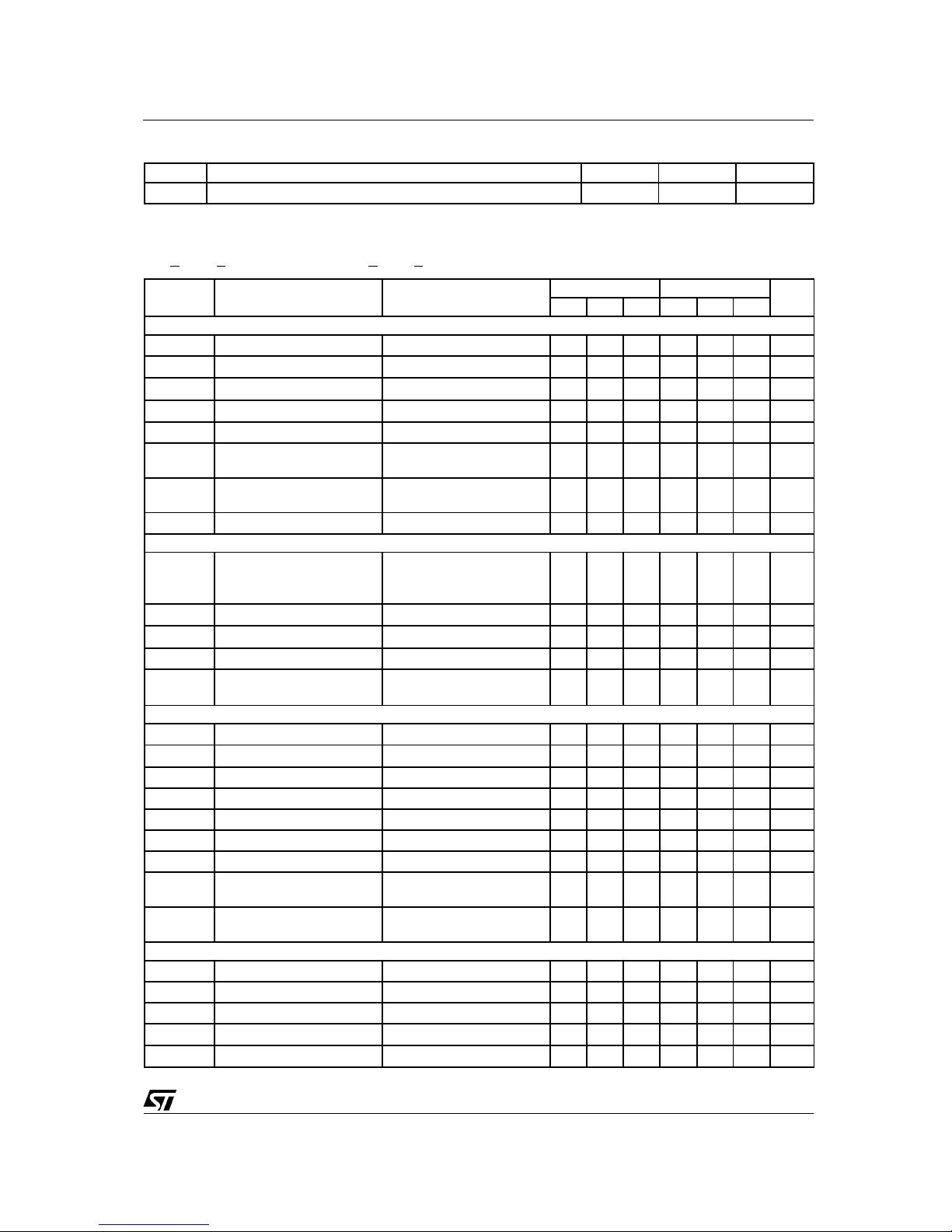
ELECTRICAL CHARACTERISTIC S ( [note 1] Unless other wise stated, these specifications apply for
-25
< T
amb
< 85°C for UC284XB; 0 < T
amb
< 70°C for UC384XB; Vi = 15V (note 5); RT = 10K; CT = 3.3nF)
Symbol Parameter Test Conditions
UC284XB UC384XB
Unit
Min. Typ. Max. Min. Typ. Max.
REFERENCE SECTION
V
REF
Output Voltage
T
j
= 25°C Io = 1mA
4.95 5.00 5.05 4.90 5.00 5.10 V
∆
V
REF
Line Regulation
12V ≤ V
i
≤ 25V
220 220mV
∆
V
REF
Load Regulation
1 ≤ I
o
≤ 20mA
325 325mV
∆
V
REF
/∆T
Temperature Stability (Note 2) 0.2 0.2
mV/°C
Total Output Variation Line, Load, Temperature 4.9 5.1 4.82 5.18 V
e
N
Output Noise Voltage
10Hz ≤ f ≤ 10KHz T
j
= 25°C
(note 2)
50 50
µ
V
Long Term Stability
T
amb
= 125°C, 1000Hrs
(note 2)
525 525mV
I
SC
Output Short Circuit -30 -100 -180 -30 -100 -180 mA
OSCILLATOR SECTION
f
OSC
Frequency
T
j
= 25°C
T
A
= T
low
to T
high
TJ = 25°C (RT = 6.2k, CT = 1nF)
49
48
225
52
–
250
55
56
275
49
48
225
52
–
250
55
56
275
KHz
KHz
KHz
∆
f
OSC
/∆V
Frequency Cha nge wit h V olt. V
CC
= 12V to 25V – 0.2 1 – 0.2 1 %
∆
f
OSC
/∆T
Frequency Change with Temp. T
A
= T
low
to T
high
–1––0.5–%
V
OSC
Oscillator Voltage Swing (peak to peak) – 1.6 – – 1.6 – V
I
dischg
Discharge Current (V
OSC
=2V) TJ = 25°C
T
A
= T
low
to T
high
7.8
7.5
8.3–8.8
8.8
7.8
7.6
8.3–8.8
8.8mAmA
ERROR AMP SECTION
V
2
Input Voltage V
PIN1
= 2.5V 2.45 2.50 2.55 2.42 2.50 2.58 V
I
b
Input Bias Current VFB = 5V -0.1 -1 -0.1 -2
µ
A
A
VOL
2V ≤ Vo ≤ 4V
65 90 65 90 dB
BW Unity Gain Bandwidth T
J
= 25°C 0.7 1 0.7 1 MHz
PSRR Power Supply Rejec. Ratio
12V ≤ Vi ≤ 25V
60 70 60 70 dB
I
o
Output Sink Current V
PIN2
= 2.7V V
PIN1
= 1.1V 2 12 2 12 mA
I
o
Output Source Current V
PIN2
= 2.3V V
PIN1
= 5V -0.5 -1 -0.5 -1 mA
V
OUT
High V
PIN2
= 2.3V;
R
L
= 15KΩ to Ground
5 6.2 5 6.2 V
V
OUT
Low V
PIN2
= 2.7V;
R
L
= 15KΩ to Pin 8
0.8 1.1 0.8 1.1 V
CURRENT SENSE SECTION
G
V
Gain (note 3 & 4) 2.85 3 3.15 2.85 3 3.15 V/V
V
3
Maximum Input Signal V
PIN1
= 5V (note 3) 0.9 1 1.1 0.9 1 1.1 V
SVR Supply Voltage Rejection
12 ≤ V
i
≤ 25V (note 3)
70 70 dB
I
b
Input Bias Current -2 -10 -2 - 10
µ
A
Delay to Output 150 300 150 300 ns
THERMAL DATA
Symbol Description Minidip SO8 Unit
R
th j-amb
Thermal Resistance Junction-ambient. max. 100 150
°
C/W
UC2842B/3B/4B/5B - UC3842B/3B/4B/5B
3/15
Page 4
Notes :
1. Max package power dissipation l imits must be respected; low duty cycle puls e techniq ues are used during test maintain T
j
as
close to T
amb
as possible.
2. These parameters, alth ough guaranteed, are not 100% tested in produc ti on.
3. Parameter measured at tri p poi nt of la tch wit h V
PIN2
= 0.
4. Gain defined as :
∆
V
PIN1
A = ; 0 ≤ V
PIN3
≤ 0.8 V
∆
V
PIN3
5. Adjust Vi above the start th reshold bef ore set ti ng at 15 V .
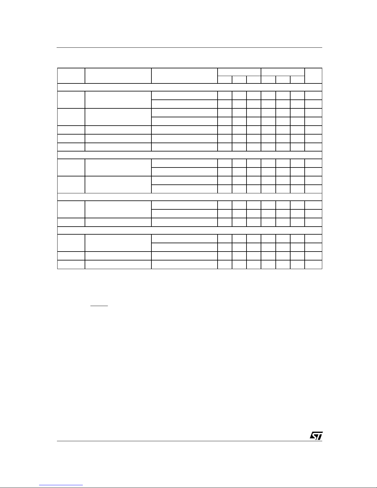
ELECT RIC AL CH ARACTERI S TI CS ( co ntinued)
Symbol Parameter Test Conditions
UC284XB UC384XB
Unit
Min. Typ. Max. Min. Typ. Max.
OUTPUT SECTION
V
OL
Output Low Level I
SINK
= 20mA 0.1 0.4 0.1 0.4 V
I
SINK
= 200mA 1.6 2.2 1.6 2.2 V
V
OH
Output High Level I
SOURCE
= 20mA 13 13.5 13 13.5 V
I
SOURCE
= 200mA 12 13.5 12 13.5 V
V
OLS
UVLO Saturation VCC = 6V; I
SINK
= 1mA 0.1 1.1 0.1 1.1 V
t
r
Rise Time
T
j
= 25°C CL = 1nF (2)
50 150 50 150 ns
t
f
Fall Time
T
j
= 25°C CL = 1nF (2)
50 150 50 150 ns
UNDER-VOLTAGE LOCKOUT SECTION
Start Threshold X842B/4B 15 16 17 14.5 16 17.5 V
X843B/5B 7.8 8.4 9.0 7.8 8.4 9.0 V
Min Operating Voltage
After Turn-on
X842B/4B 9 10 11 8.5 10 11.5 V
X843B/5B 7.0 7.6 8.2 7.0 7.6 8.2 V
PWM SECTION
Maximum Duty Cycle X842B/3B 94 96 100 94 96 100 %
X844B/5B 474850474850 %
Minimum Duty Cycle 0 0 %
TOTAL STANDBY CURRENT
I
st
Start-up Current Vi = 6.5V for UCX843B/45B 0.3 0.5 0.3 0.5 mA
V
i
= 14V for UCX842B/44B 0.3 0.5 0.3 0.5 mA
I
i
Operating Supply Current V
PIN2
= V
PIN3
= 0V 12 17 12 17 mA
V
iz
Zener Voltage Ii = 25mA 30 36 30 36 V
UC2842B/3B/4B/5B - UC3842B/3B/4B/5B
4/15
Page 5
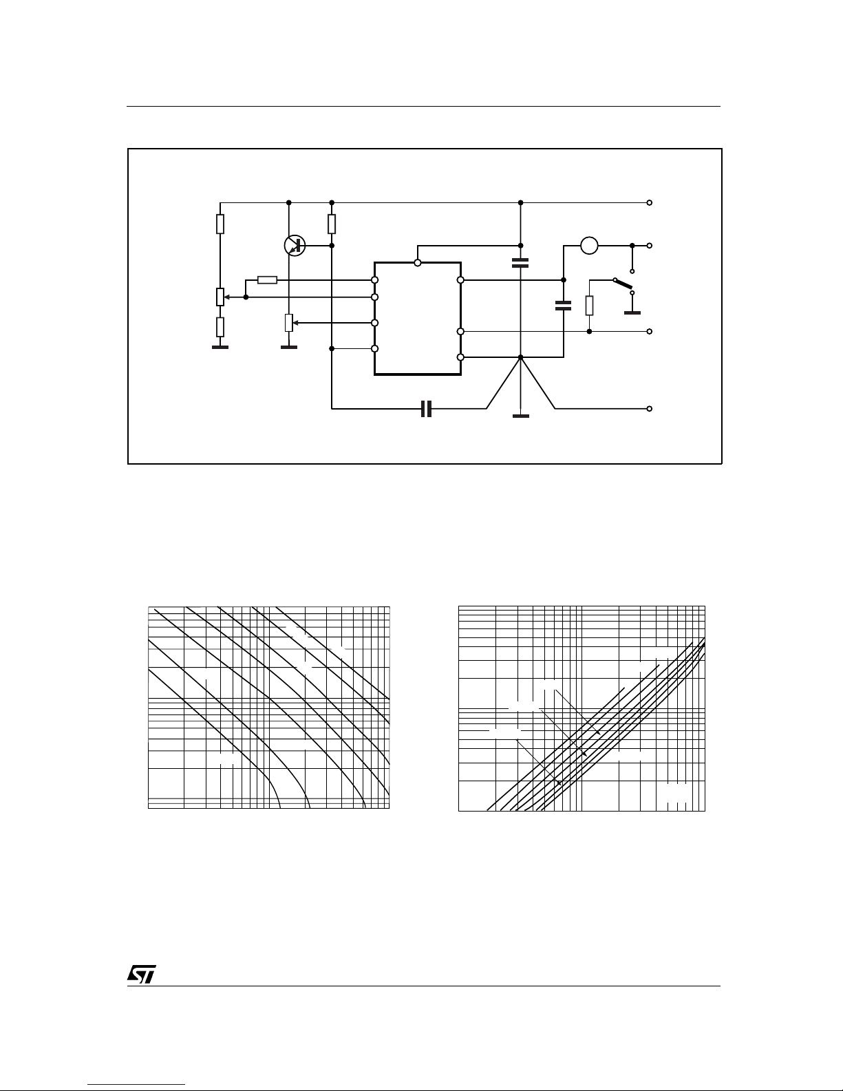
Figure 1: Open Loop Te st Ci rc ui t.
R
T
A2N2222
4.7KΩ
1KΩ
ERROR AMP.
ADJUST
4.7KΩ
5KΩ
I
SENSE
ADJUST
100KΩ
COMP
V
FB
I
SENSE
RT/C
T
1
2
3
4
C
T
7
6
5
8
V
REF
V
i
OUTPUT
GROUND
0.1µF
0.1µF
V
REF
V
i
OUTPUT
GROUND
1W
1KΩ
D95IN343
High peak curr ents associat ed with capac itive loads
necessitate careful grounding techniques. Timing
and bypass capacitors should be connected close
to pin 5 in a si ngle point ground. The transis tor and
5 KΩ potentiomet er are used to sample the oscillato r
waveform a nd ap ply an adjustable ra m p to pin 3 .
10K 20K 30K 50K 100K 200K 300K 500K f
OSC
(KHz)
1
2
5
10
20
50
D95IN333
CT=10nF
CT=5nF
CT=2nF
C
T
=1nF
C
T
=500pF
C
T
=200pF
C
T
=100pF
Vi=15V
T
A
=25˚C
RT
(KΩ)
0.8
Figure 2: Timing Resistor vs. Oscillator Fre-
quency
10K 20K 30K 50K 100K 200K 300K 500K fOSC(KHz)
1
2
3
5
10
20
30
50
%
CT=10nF
CT=5nF
CT=2nF
CT=1nF
CT=500pF
CT=200pF
CT=100pF
D95IN334
Vi=15V
T
A
=25˚C
Figure 3: Output Dead-Time vs. Oscillator Fre-
quency
UC2842B
UC2842B/3B/4B/5B - UC3842B/3B/4B/5B
5/15
Page 6

-55 -25 0 25 50 75 100 TA(˚C)
7.0
7.5
8.0
8.5
I
dischg
(mA)
D95IN335
Vi=15V
V
OSC
=2V
Figure 4: Oscillator Discharge Current vs. Tem-
perature.
1235
40
50
60
70
80
90
D
max
(%)
0.8 RT(KΩ)
D95IN336
Vi=15V
C
T
=3.3nF
T
A
=25˚C
I
dischg
=7.5mA
I
dischg
=8.8mA
Figure 5: Maximum Output Duty Cycle vs. Tim-
ing Resistor.
10 100 1K 10K 100K 1M f(Hz)
-20
0
20
40
60
80
(dB)
180
150
120
90
60
30
φ
D95IN337
Vi=15V
V
O
=2V to 4V
R
L
=100K
T
A
=25˚C
Gain
Phase
Figure 6: Error Amp Open-Loop Gain and
Phase vs. Frequency.
0246V
O
(V)
0.0
0.2
0.4
0.6
0.8
1.0
V
th
(V)
D95IN338
Vi=15V
TA=-40˚C
TA=125˚C
TA=25˚C
Figure 7: Current Sense Input Threshold vs. Er-
ror Amp Output Voltage.
0 20406080100I
ref
(mA)
D95IN339
0
10
20
30
40
50
60
Vi=15V
TA=-40˚C
TA=125˚C
T
A
=25˚C
Figure 8: Reference Voltage Change vs.
Source Current.
-55 -25 0 25 50 75 100 TA(˚C)
D95IN340
50
60
70
80
90
100
I
SC
(mA)
Vi=15V
R
L
≤0.1Ω
Figure 9: Reference Short Circuit Current vs.
Temperature.
UC2842B/3B/4B/5B - UC3842B/3B/4B/5B
6/15
Page 7

0 200 400 600 IO(mA)
0
1
2
3
-2
-1
V
sat
(V)
D95IN341
Vi=15V
80µs Pulsed Load 120Hz Rate
TA=-40˚C
TA=25˚C
V
i
TA=-40˚C
TA=25˚C
GND
Sink Saturation
(Load to V
i
)
Source Saturation
(Load to Ground)
Figure 10: Output Saturation Voltagevs. Load
Current.
0 102030V
i
(V)
0
5
10
15
20
I
i
(mA)
UCX843/45
UCX842/44
RT=10K
C
T
=3.3nF
V
FB
=0V
I
Sense
=0V
T
A
=25˚C
D95IN342
Figure 11: Supply Current vs. Supply Voltage.
Figure 12: Output Waveform. Figure 13: Output Cross Conduction
5V REG
OSCILLATOR
PWM
CLOCK
8
4
5
6
R
T
C
T
GND
OUTPUT
7
V
i
I
D
CT
OUTPUT
LARGE R
T
/SMALL C
T
CT
OUTPUT
SMALL R
T
/LARGE C
T
D95IN344
Figure 14: Oscillator and Output Waveforms.
Vi =15V
C
L
= 1.0nF
T
A
= 25°C
90%
10%
50ns/DIV
Vi =30V
C
L
= 15pF
T
A
= 25°C
V
O
I
CC
100ns/DIV
100mA/DIV
20V/DIV
UC2842B/3B/4B/5B - UC3842B/3B/4B/5B
7/15
Page 8

Figure 15 : Error Amp Conf ig ura t ion.
Z
i
Z
f
1mA
2
1
V
FB
COMP
2.5V
D95IN345
+
-
Figure 16 : Under Voltage Lo c ko ut .
UC3842B
UC3844B
UC3843B
UC3845B
16V 8.4V
10V 7.6V
V
ON
V
OFF
V
i
ON/OFF COMMAND
TO REST OF IC
7
<0.5mA
<17mA
I
CC
V
CC
V
OFFVON
D95IN346
Figure 17 : Current Sense Cir c uit .
ERROR
AMPL.
2R
R1V
CURRENT
SENSE
COMPARATOR
1
CURRENT
SENSE
COMP
CR
S
R
3
5
GND
I
S
D95IN347
Peak curre nt (is) is determined by the formu la
1.0 V
I
S max
≈
R
S
A small RC fi lter ma y b e re quir ed to suppres s switch transi ent s .
During UVLO, the Output is low
UC2842B/3B/4B/5B - UC3842B/3B/4B/5B
8/15
Page 9

Figure 18 : Slope Compe ns at ion T ec hni que s.
R
S
R
1
I
S
R
SLOPE
C
T
R
T
V
REG
8
R
T/CT
I
SENSE
4
3
5
GND
R
S
R
1
I
S
R
SLOPE
C
T
R
T
V
REG
8
R
T/CT
I
SENSE
4
3
5
GND
D95IN348
Figure 19 : Isolated MOSF E T Drive and Cu rrent Transform er Se ns ing.
7
6
COMP/LATCH
ISOLATION
BOUNDARY
D95IN349
5.0V
ref
V
CC
+
-
+
-
Q
S
R
+
-
3
R
R
S
N
S
C
V
in
Q1
N
P
VGS Waveforms
+
0
+
0
--
50% DC 25% DC
I
pk
=
V
(pin 1)
-1.4
3R
S
N
S
N
P
()
UC3842B
UC3842B
UC2842B/3B/4B/5B - UC3842B/3B/4B/5B
9/15
Page 10

Figure 20 : Latched Shutdown.
D95IN350
BIAS
+
EA
R
+
OSC
2N
3905
2N
3903
1mA
R
R
2R
1
2
8
4
SCR must be selected for a holding current of less than 0.5mA at T
A(min)
.
The simple two transistor circuit can be used in place of the SCR as shown. All resistors are 10K.
5
D95IN351
+
EA
R
i
+
1mA
R
d
R
2R
5
C
f
R
f
1
2
From V
O
2.5V
+
EA
R
P
+
1mA
R
d
R
2R
5
C
f
R
f
1
2
From V
O
2.5V
Error Amp compensation circuit for stabilizing any current-mode topology except
for boost and flyback converters operating with continuous inductor current.
C
P
R
i
Error Amp compensation circuit for stabilizing current-mode boost and flyback
topologies operating with continuous inductor current.
Figure 21: Error Amplifier Compensation
UC2842B/3B/4B/5B - UC3842B/3B/4B/5B
10/15
Page 11

D95IN353
+
-
+
R
A
1
7
f =
R
BIAS
OSC
C
6
V
REF
RR
B
+
-
+
EA
R
2R
R
S
Q
84
5
2
3
5K
5K
5K
NE555
8
4
2
1
5
TO ADDITIONAL
UCX84XAs
1.44
(R
A
+ 2RB)C
D
max
=
R
B
RA + 2R
B
Figure 23: External Duty Cycle Clamp and Multi Unit Synchronization.
D95IN352
+
EA
+
R
2R
5
R
T
1
2
EXTERNAL
SYNC INPUT
The diode clamp is required if the Sync amplitude is large enough to cause
the bottom side of C
T
to go more than 300mV below ground
R
BIAS
OSC
C
T
0.01µF
47Ω
4
8
V
REF
R
Figure 22: External Clock Synchronization.
UC2842B/3B/4B/5B - UC3842B/3B/4B/5B
11/15
Page 12

D95IN354
+
R
BIAS
OSC
C
R
+
-
+
EA
R
2R
R
S
Q
8
4
2
1
5
1mA
1V
+
-
5V
ref
1MΩ
Figure 24: Soft-Start Circuit
D95IN355
+
R
BIAS
OSC
C
R
+
-
+
EA
R
2R
R
S
Q
8
4
2
1
5
1mA
1V
+
-
5V
ref
R2
R1
V
Clamp
+
-
Comp/Latch
7
R
S
V
CC
Q1
V
in
7
6
5
BC109
V
CLAMP
= ·
R
1
R1 + R
2
where 0 <V
CLAMP
<1V I
pk(max)
=
V
CLAMP
R
S
Figure 25: Soft-Start and Error Amplifier Output Duty Cycle Clamp.
UC2842B/3B/4B/5B - UC3842B/3B/4B/5B
12/15
Page 13

DIM.
mm inch
MIN. TYP. MAX. MIN. TYP. MAX.
A 1.75 0.069
a1 0.1 0.25 0.004 0.010
a2 1.65 0.065
a3 0.65 0.85 0.026 0.033
b 0.35 0.48 0.014 0.019
b1 0.19 0.25 0.007 0.010
C 0.25 0.5 0.010 0.020
c1 45° (typ.)
D (1) 4.8 5.0 0.189 0.197
E 5.8 6.2 0.228 0.244
e 1.27 0.050
e3 3.81 0.150
F (1) 3.8 4.0 0.15 0.157
L 0.4 1.27 0.016 0.050
M 0.6 0.024
S8° (max.)
(1) D and F do not include mold flash or protrusions. Mold flash or
potrusions shall not exceed 0.15mm (.006inch).
SO8
OUTLINE AND
MECHANICAL DATA
UC2842B/3B/4B/5B - UC3842B/3B/4B/5B
13/15
Page 14

Minidip
DIM.
mm inch
MIN. TYP. MAX. MIN. TYP. MAX.
A 3.32 0.131
a1 0.51 0.020
B 1.15 1.65 0.045 0.065
b 0.356 0.55 0.014 0.022
b1 0.204 0.304 0.008 0.012
D 10.92 0.430
E 7.95 9.75 0.313 0.384
e 2.54 0.100
e3 7.62 0.300
e4 7.62 0.300
F 6.6 0.260
I 5.08 0.200
L 3.18 3.81 0.125 0.150
Z 1.52 0.060
OUTLINE AND
MECHANICAL DATA
UC2842B/3B/4B/5B - UC3842B/3B/4B/5B
14/15
Page 15

Information furnished is believed to be accurate and reliable. However, STMicroelectronics assumes no responsibility for the consequences of use of such inform ation nor for any i nfringement of patents or other rights of third parties whic h may result from its use. No
license is granted by implication or otherwise under any patent or patent rights of STMicroelectronics. Specification mentioned in this
publication are subject to change without notice. This publication superse des and replaces all information previously supplied. STMicroelectronics products are not authorized for use as critical components in life support devices or systems without express writ ten
approval of STMicr oelectronic s.
The ST logo is a register ed tradem ark of STMic roelec tronics
© 1999 STMicroelectr onics – Pr inted in Ital y – All Ri ghts Reserv ed
STMicroelectronics GR OUP OF COM PANIES
Australia - Brazil - Canada - Chi na - F rance - Germany - Italy - J apan - Korea - Mal aysia - M alta - Mex ico - Mor occo - The N ether lands -
Singapore - Spain - Sweden - Swi tzerland - T aiwa n - Thailand - U nited K ingdom - U. S.A.
http://www.st.co m
UC2842B/3B/4B/5B - UC3842B/3B/4B/5B
15/15
 Loading...