

APPLICATION NOTE
UC3842 PROVIDES LO W-COST CURREN T-MODE CONT ROL
The fundam ental challeng e of power suppl y design
is to simultaneously realize two conflicting objectives : good electrical performance and low cost. The
UC3842 is an integrated pulse width modulator
(PWM) designed with both these objectives in mind .
This IC provides desi gner s an inexpens ive c ont roller with which they can obtain all the performance
advant age s of cur rent - m ode o per ati on . In ad diti on ,
the UC3 842 is optimiz ed for efficie nt power sequ encing of off-line converters and for driving increasingly popular POWERMOS.
This application note gives a functional description
of the UC3 842 and sug gests how to incorpor ate the
IC into practical power supplies. A review of currentmode control and its benefits is included and me-
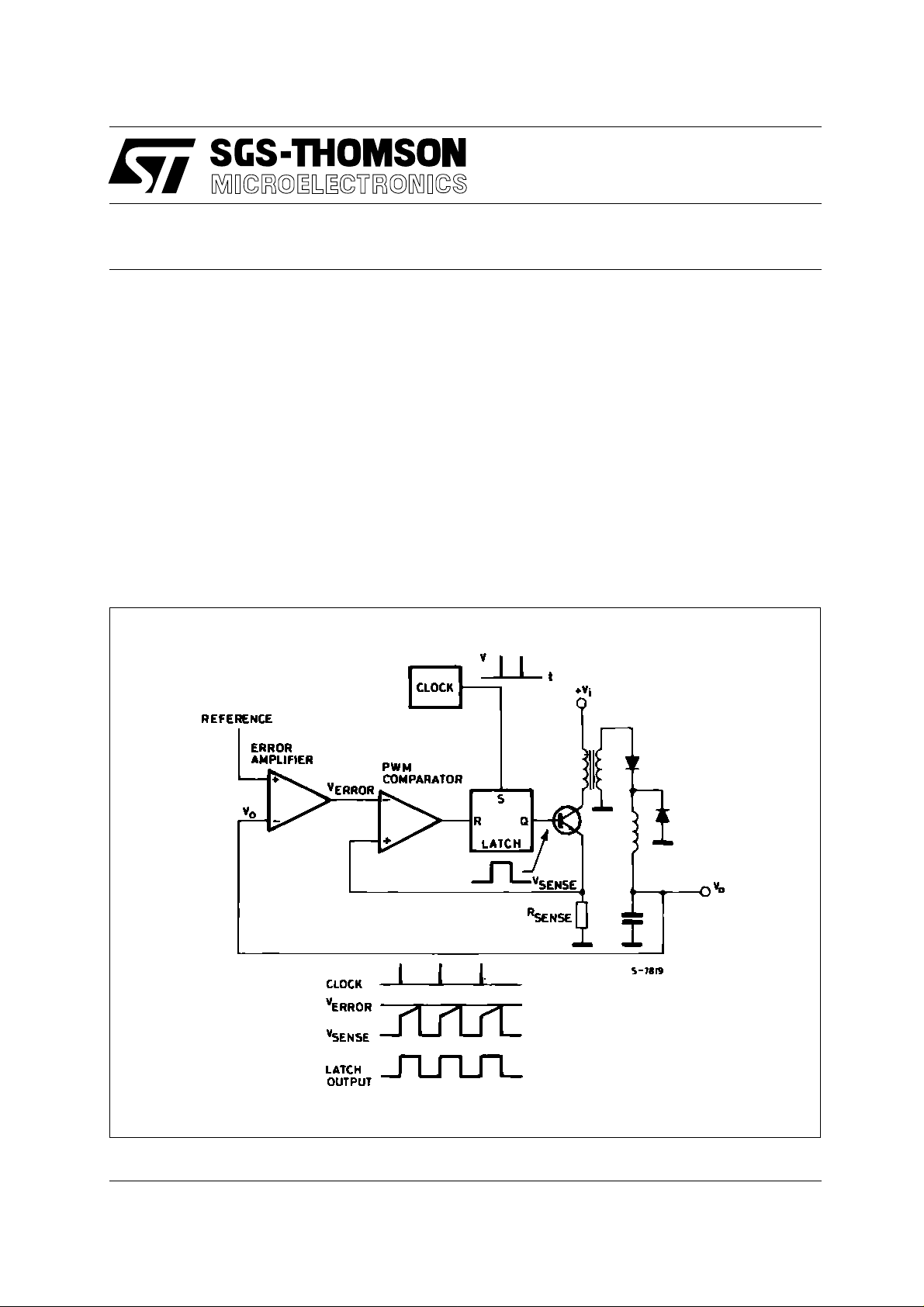
Figure 1 : Two-loo p Cur r ent-mode Cont ro l Sys tem .
thods of avoiding com mon pitfalls dis cussed. The final sect ion pr es ent s des ig ns of tw o po wer s u p pli es
utilizing UC3842 control.
CURRENT-MODE CONTROL
Figure 1 shows the two-loop current-mode control
system in a typical buck regulator application. A
clock s ignal initia tes power pu lses at a fi xed freque ncy. The termination of each pulse occurs when an
analog of the inductor current reaches a threshold
establish e d by the error si g nal . I n t his way the er r or
signal actually controls peak inductor current. This
contrasts with conventional schemes in which the
error signal directly controls pulse width without regard to induc tor current.
AN246/1188
1/16
APPLICATION NOTE
Several performance advantages result from the
use of current-mode control. First, an input voltage
feed-forward characteristic is achieved ; i.e., the
control circ uit instantaneously corr ects for input voltage vari ations withou t using up any o f the erro r amplifier’s dynami c range. Ther ef or e, line re gu lation i s
excel lent and the error amp lifier can be dedic ated to
correc ting for load v ariat io ns excl us ively .
For converters in which inductor current is continuous, cont r olli ng peak curre nt is nea rly equ iv alen t
to controlling average current. Therefore, when
such converters employ current-mode control, the
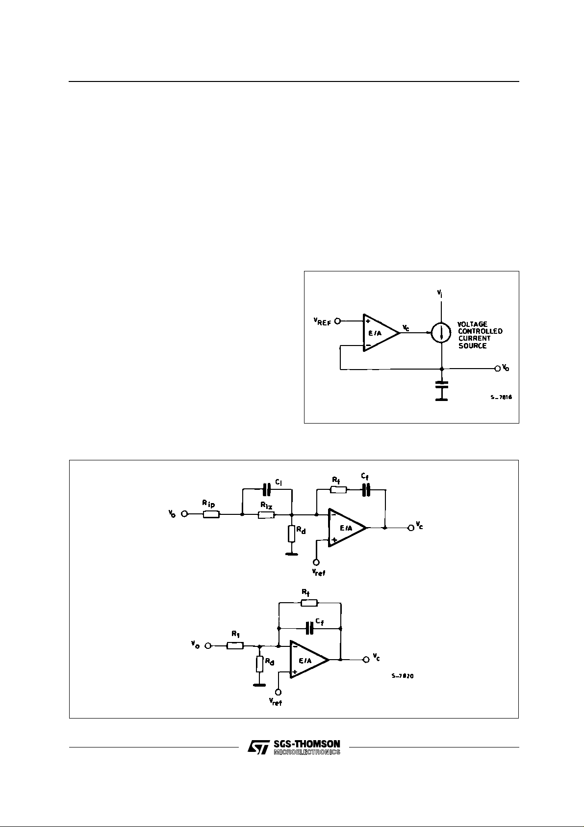
inductor c an be tr eat e d as an e rr or -v o l tage- controlled-current-source for the purposes of small-signal
analysis . This is illu strated by fi gure 2. The t wo-pole
control-to-outp ut frequency respons e of these co nverters is reduc ed to a sing le pole (filter capa citor i n
parallel wit h l o ad) res p o ns e.
One resul t is th a t the e rror amplif ie r compen sati on
can be designed to yield a stable closed-loop co nverter response with greater gain-bandwidth than
would be possible with pulse-width control, giving
the supply improved s mall-signal dynami c response
to changing loads. A second result is that the error
amplifi er compensation c ircuit becomes s impler and
better behaved, as illustrated in figure 3. Capacitor
C
and resistor Riz in figure 3a add a low frequency
i
zero which cancels one of the two control-to-output
poles of no n-curr ent-m ode c onvert ers. For lar ge-si-
gnal load changes, in which converter response is
limited by inductor slew rate, the error amplifier will
saturate while the inductor is catching up with the
load. Dur ing this ti me, C
will charge to an a bnormal
i
level. W hen the inductor current reache s its required
level, the voltage on C
in supply output vol-tage. The recovery time is R
causes a corresponding err or
i
iz Ci
which may be milleseconds. However, the compensation netw ork of figur e 3 b can b e us ed where current-mode control has elimi nated the induc tor pole.
Large-signal dynamic response is then greatly improve d due to the a b senc e of C
.
i
Figure 2 : Inductor Looks Like a C urr en t Sou rce to
Small Signals.
,
Figure 3 : Required Error Am plif ier C ompen sa tion for Continuou s Induc tor Curr ent De si gns using (a) Duty -
cycle C ont ro l and (b ) Cur re nt-m o de C ont ro l.
(a)
(b)
2/16
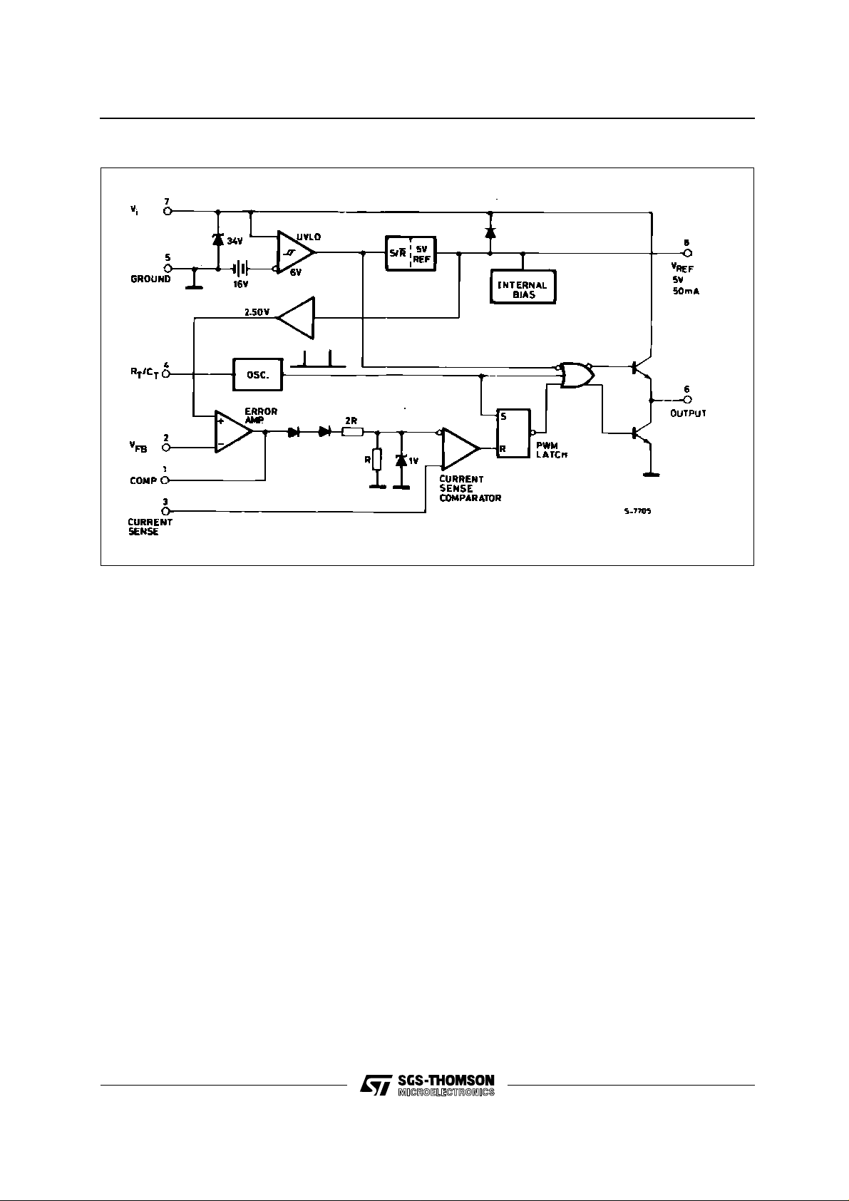
Figure 4 : UC3842 Block Diagram.
APPLICATION NOTE
Current limiting is simplified with current-mode control. Puls e-by-p ulse limi ting is, of course, in herent i n
the control schem e. Furtherm o re, a n upper li m it on
the peak curr ent can b e es tablished by si mply clamping the error voltage. Accurate current limiting allows optimization of magnetic and power
semiconductor elements while ensuring reliable
supply oper ati o n.
Finally, current-mode controlled power stages can
be operated in parallel with equal current sharing.
This opens the p ossib ility o f a m odul ar a ppro ac h to
power suppl y d es ign.
FUNCTIONAL DESCRIPTION
A block diag ram of th e UC3842 appear s in fi gure 4.
This IC will op erate from a low impedanc e DC source of 10 V to 30 V. Operation between 10 V and 16
V requires a start-up bootstr ap to a volt age gre ater
than 16 V in order to overcome the undervoltage lockout. V
is interna lly clamped to 34 V for operation
CC
from higher voltage current-limited sources
≤ 30 mA).
(I
CC
UNDER-VOLTAGE LOCKOUT (UVLO)
This c ircuit insures that V
is adequate to m ake the
CC
UC3842 fully ope rational before enabling the out put
stage. Figure 5a shows that the UVLO turn-on and
turn-off threshold s are fixed internally at 16 V and 10
V respec tively. The 6 V hysteresis prevents V
CC
oscillations during power sequencing. Figure 5b
shows supp ly current requirem ents. Start-up curre nt
is less than 1 mA for efficien t bootstrapp ing from the
rectified input of an off-line converter, as illustrated
by figure 6. During normal circuit operation, V
developed from auxiliar y winding W
C
. At star t-up, however , CIN must be charged to 16
IN
V through R
. With a start-up current of 1 mA, R
IN
with D1 and
AUX
CC
is
can be as large as 100 k Ω and sti ll charg e CIN when
V
= 90 V RMS (low line). Po wer dissip ation in R
AC
would then be less than 350 mW even under high
line (V
= 130 V RMS) conditions.
AC
During UVLO, the U C3842 o utput driver is bias ed to
a high impeda nce state. H owever, leakage currents
(up to 10 µA), if not shunted to ground, could pull
high the gate of a POWERM OS. A 100 kΩ shunt, as
showi ng in fi gure 6, will h old th e gate v oltag e be low
1V.
IN
IN
3/16

APPLICATION NOTE
Figure 5 : (a) Under-vol tage Lo cko u t and (b) Su pply Curr ent Requir eme nts.
(a) (b)
Figure 6 : Providing Power to the UC3842.
OSCILLATOR
The UC3842 oscillator is program me d as shown in
figure 7a. Oscillator timing capacitor C
from V
(5 V) through RT, and discharged by an
REF
is charged
T
internal c urrent source. Charge a nd discharge time s
are given by :
t
≈ 0.55 RT C
c
4/16
T
≈ RT CT ln ( )
t
d
frequency, then, is : f =
0.0063 RT – 2.7
0.0063 R
– 4.0
T
1
t
+ t
c
d
For RT > 5 kΩ, td is small compared to tc, and :
f ≈≈
11.8
0.55 R
T CT
RT C
T

APPLICATION NOTE
During the discharge ti me, the internal cloc k signal
blan ks the output to the low stat e. Therefor e, t
maximum duty cycle (D
t
D
MAX
c
== 1 –
t
+ t
c
d
MAX
t
d
τ
) to :
limits
d
where τ = 1/f = switching period.
The timing capacitor discharge current is not tightly
controlled, so t
may vary somewhat over temp era-
d
ture and fro m unit t o unit. T herefor e, when v ery pre cise duty cycle limiting is required, the circuit of figure 7b is reco m m end ed.
One or more UC3842 osc illators c an be sy nc hroni zed to an ex ternal clock as s hown in figur e 8. Nois e
immunity is enhanced if the free-running oscillator
frequency (f = 1/(t
20 % less than the clock frequency.
~
+ td)) is programmed to be
c
Figu re 7 : (a) Oscilla tor Timing C onne cti ons and (b) Cir c uit f or Li m iting Dut y Cy cl e.
(a) (b)
Figure 8 : Synchronizatio n to an E xte rn al Cl oc k.
ERROR AMPLIFIER
The error amplifier (E/A) configuration is shown in
figure 9. The non-inverting input is not brought out
t
D
MAX
= 0.693 (RA + RB) C
t
H
= 0.693 RB C
t
L
c
=
(t
+ tL)
H
to a pin, but is internally biased to 2.5 V ± 2 %. The
E/A output is availab le at pin 1 for externa l compensation, allowing the user to control the converter’s
closed-lo op freque nc y respon se.
Figure 10a s ho w s an E /A c o m pe ns at io n ci rcu i t su itable for stabilizing any current-mode controlled topology except for flyback and boost converters
operating with continuous inductor current. The feedback co mpon ent s add a pole to th e l oop transfe r
function at f
= 1/2 πRf Cf. Rf and Cf are chosen so
p
that this pole canc els the zero of t he out put fil ter c apacito r ESR in the power circu it. R
and Rf fix the low-
i
frequency gain. They are chosen to pr ovide as much
gain as po ssi ble whil e s til l al lowi ng th e p ole for m ed
by the output filter capacitor and load to roll off the
loop gain to unity (0dB) at f ≈ f
switching
/4. This technique insures converter stability while providing good
dynamic response.
Continuous-i nductor-curr ent boost and flyback converters each have a right-half-plane zero in their
transfer funct io n. An a ddi ti ona l comp ens at io n pole
is needed to roll off loop gain at a frequency less than
that of the RHP zero. R
and Cp in the circuit of figure
p
10b provide t his pol e.
5/16

APPLICATION NOTE
The E/A output will source 0.5 mA and sink 2 mA. A
lower li m it fo r R
R
≈ == 7 kΩ
f (MIN)
is given by :
f
V
E/A OUT(max)
– 2.5 V 6 V – 2.5 V
0.5 mA 0.5 m A
E/A input bias current (2 µA m ax ) fl o ws th ro ugh R
resulting in a DC error in output voltage (V
) given
o
by :
o(max)
= (2 µA) R
i
∆ V
Figure 9 : UC3842 Error Amplifier.
It is therefore desirable to keep the value of Ri as low
as possible.
Figure 11 sh ows the o pen-loop frequency r esponse
of the UC3842 E/A . The ga in rep rese nt an upper li mit on the gain of the compensated E/A. Phase lag
,
i
increases rap idly as freq uency exc eeds 1 M Hz due
to second-order pole s at ∼ 10 MHz and above.
Figure 10 : (a) Error Amplifier Compensation Addi-
tion Pole and (b) Needed for Continu
ous Inductor-current Boost ad Flyback.
(a)
(b)
Figure 11 : Error Amplifier Open-loop Frequency
Response.
6/16

APPLICATION NOTE
CURRENT SENSING AND LIMITING
The UC3842 current sense input is configured as
shown in figur e 12. Current-to-v oltage convers ion is
done external ly w ith gr ound-refer enced r esist or R
Under normal operat ion the peak voltage across R
is controlled by the E/A according to the following relation :
V
– 1.4 V
(pk) =
V
RS
where : V
R
can be connecte d to the p o wer c ir cu it dir ec t ly or
S
C
3
= control voltage = E/A output voltage.
C
through a current transformer, as figure 13 illus trates. While a di rect co nnectio n is simpler , a trans former can reduce power dissipation in R
, reduce
S
errors cau sed by the ba se current, and pr ovide level
shifting to eliminate the restraint of ground-reference sensing . The relation bet ween V
and peak
C
current in the p ower sta ge is giv en by :
V
(pk) N
= N ( ) = (VC – 1.4)
i
(pk)
RS
R
S
3 R
S
where : N = current sense transf or m er tur ns ra ti o.
= 1 when transformer not us ed.
Figure 12 : Current Sensing.
For purposes of small-signal analysis, the controlto-sensed-c urrent gain is :
i
(pk)
V
.
S
S
C
When sensing cu rrent in ser ies with the power tran-
N
=
3 R
S
sistor, as shown in figure 13, current waveform will
often ha v e a l a r g e spike at its lead ing edg e. T h is i s
due to rectifi er re cove ry and/ or i nterwind ing c apacitance in th e power transfor mer. If unatten uated, this
transient can prematurely terminate the output pulse. As shown, a sim ple RC filter is us ually adequa te
to suppress this spike. The RC time constant should
be approxi mately equal to the cur rent spi ke duration
(usually a f ew h u ndr ed na nos ec o n ds ).
The inverting input to the UC3842 current-sense
comparator is internally clam p ed to 1 V (figure 12).
Current lim iting occurs if the volt age at pin 3 reaches
this threshold value, i.e. the current limit is defined
by :
.
N
i
MAX
=
1 V
R
S
7/16

APPLICATION NOTE
Figure 14 : Output Cross-co n d uction.Figure 13 : Transformer-coupled Current Sensing.
TOTEM-POLE OUTPUT
The UC3842 has a single totem-pole output. The
output transis tors can be operated t o ± 1 A peak current and ± 200 mA average current. The peak cur-
rent is self-limiting, so no series current-limiting
resistor is n eeded w hen dr ivin g a power MOS gat e.
Cross-co nd uc tion be tw een the out pu t tran sist ors is
minimal, as figur e 14 shows. The averag e added power due to cross-conduction with V
= 30 V is onl y
i
80 mW at 200 kHz.
Figures 15-17 show suggested circuits for driving
POWERMOS and bipolar transistors with the
UC3842 output. The simple circuit of figure 15 can
be used wh en the cont rol IC is not el ectric ally iso lated from the power MOS. Series resistor R
provides
1
damping for a parasitic tank circuit formed by the po wer MOS i nput capacitanc e and any seri es wiring inductance. Resistor R
shunts output leakage
2
currents (10 µA maximum) to ground when the under-voltage lockout is active. Figure 16 shows an
isolated power M OS drive circui t which is appropria te when the drive signal must be levelshifted or transmitted across an isolation boundary. Bipolar
transistors can be driven effectively with the circuit
of figu re 17. Resist ors R
base curren t. Capacitor C
and R2 fix the on-state
1
provides a negative base
1
current pulse to remove stored charge at turn-off.
SHUTDOWN TECHNIQUES
Shutdown of the UC3842 can be accomplished by
two methods ; either raise pin 3 above 1 V or pull pin
1 below 1 V. Either method causes the output of the
PWM compara tor to be high (refer to block diagram ,
figure 4). The PWM latch is reset dominant so that
the output will remain low until the first clock pulse
follow ing remo val of the shutdo wn sign al at p in 1 or
pin 3. As shown in figure 18, an externally latched
shutdown can be accompli shed by addin g an SCR
which will be reset by cycling V
below the lower
CC
under-vo ltage lockout threshold (10 V). At this poin t
all interna l bias is rem oved, allowing the SCR t o reset.
Figure 15 : Direct POWERM OS Dr iv e.
PWM LATCH
This flip-flop, sho wn i n figur e 4, ensures t hat on ly a
single pulse appears at the UC3842 output in any
one oscillator period. Excessive power transistor
dissipation an d potential s aturation o f magnetic elements are ther eby av erte d.
8/16

Figure 16 : Isolated POWE RMOS Drive.
Figure 17 : Bipolar Drive with Negative Turn-of f Bias.
APPLICATION NOTE
AVOIDING COMMON PITFALLS
Current-mode controlled converters can exhibit performance pec ul iarities under certain operating conditions. This section explains these situations and
how to correct them when using the UC3842.
SLOPE COMPENSATION PREVENTS INSTABILITIES
It is well documented that current-mode controlled
converters can exhibit subharmonic oscillations
when operated at duty cycles greater than 50 %.
Fortunately, a simple technique (usually requiring
only a single res istor to implem ent) exists which corrects this problem and at the same time improves
converter perf ormance in other respec t s. This "sl ope compensation" tec hnique is described in detail in
Reference 6. It should be noted that "duty cycle"
here refers to outp ut pulse width divide d by oscillator
period, even in push-pull designs where the transformer period is twic e t hat of th e os c illa t or. Th e refore, push-pull circuits will almost always require
slope compensation to prevent subharmonic oscillation.
9/16

APPLICATION NOTE
Figure 18 : Shutdown Achieved by
(a) Pulling P in 3 Hig h
(b) Pulling P in 1 Low .
(a)
(b)
Figure 19 illustrates th e slope compensation t echnique. In figure 19a the uncompensated control voltage and current sense waveforms are shown as a
reference. Cur rent is often s ensed in s eries with the
switching transistor for buck-derived topologies. In
this case, the current sense sign al does not track the
decaying indu ctor curr ent when the t ransis tor is off,
so dashed lines indicate this inductor current. The
negativ e inductor current slope is fixed by the val ues
of output voltag e (V
di
dt L L L
where : V
V
L
L
== =
= forward voltage drop across the free-
F
wheeling diode. The actual slo pe (m
) and inductance (L) :
o
– VF – V
o
– (VF + Vo)
) of the das hed
2
lines in figure 19a is given by :
R
=
m
2
where : R
di
S
.
Ndt NL
and N are defined as the "Current Sen-
S
L
=
– RS (VF + Vo)
sing" section of this pape r.
In figure 19b, a sawtooth voltage with slope m has
been added to the control signal. The sawtooth is
synchronized with the PWM clock, and practice is
most easily derived from the control chip oscillator
as shown in figure 20a. The s awtooth slope in figu re
19b is m = m
/2. This particular s lope value is sig ni-
2
ficant in that it yields "perfect" current-mode control ;
i.e. with m
/2 the average inductor current follows
2
the control signal so that, in the small-signal analysis, the inductor acts as a controlled current source.
All current-mode controlled converters having continuous inductor current therefore benefit from this
amount of slope compe nsation , whether or not the y
operate above 50 % duty.
More slope is need ed to prev ent subh armonic oscillations at h igh d uty cy cles. Wi th slope m = m
, such
2
oscillati ons wil l not oc cur if the error a mplifie r gain
(A
) at half the s witching fre quency (fs/2) is kept
V(E/A)
below a thres h old v al ue (r ef er enc e 6 ) :
π 2 C
A
V (E/A)
where : C
<
m = m2
/2
f = f
s
= sum of filter and load c apac it a nc e
o
τ = 1/f
s
O
4 τ
Slope co mpensatio n can also improve th e noise im munity of a current-mode controlled supply. When
the inductor ripple current is small compared to the
averag e current (as in figure 19a), a small amount
of noise on the current sens e or contro l signals can
cause a large pulse-width jitter. The magnitude of
this jitter varies inversely with the difference in slope
of the two sign als. B y adding slope as in figu re 19b,
the jitte r is re duc ed. I n noi sy envi ron ments it is sometimes ne cessar y to add s lope m > m
in order to
2
correct this problem. Howev er , as m increases beyond m = m
/2, the circu it becomes l ess perfect ly
2
current contro lled. A complex trad e-off is then required ; for very noisy circuits the optimum amount of
slope com pen sa t ion is b e st found em pir ic a l ly .
Once the r equire d slo pe is de termi ned, t he value o f
R
3 m =
in figure 20a can be c alc ula t ed :
SLOPE
∆V
∆ t
RAMP
RAMP
.
A
0.7 V R
=( ) =( )
V(E/A)
τ/2 ZF | f
SLOPE
s
1.4 R
SLOPE
τ ZF | fs
3 m τ
R
=(Z
SLOPE
where : Z
1.4
| fs is the E/A feedback impedance at the
F
| fs) = 2.1 . m . τ . ZF | f
F
s
switching frequency.
For m = m
R
SLOPE
L : ∆τRAMP
= 1.7 τ () Z
Rs (VF + VO)
NL
| f
F
s
10/16

Figure 19 : Slope Compen sati on Wa ve form s :
(a) No Comp.
(b) Comp. Added to Control Voltage.
(c) Comp. Added to Current Sens e.
APPLICATION NOTE
Note that in order for the error amplif ier to accurately
replicate the ramp, Z
quency ra nge f
must be constant over the fre-
F
to at least 3 fs.
s
In order to elim i n ate t his las t co ns tra i nt, a n alt er n ative met hod of slope compensati on is shown in figures 19c and 20b. Here the artificial slope is added
to the current sense waveform rather than subtracted from the control signal. The magnitude of the added slope still relates to the downslope of inductor
current as described above. The requirement for
R
m = ( ) = ( )
R
is now :
SLOPE
∆V
RAMP
∆t
RAMP
=– R
SLOPE
Rf + R
1.4 R
f
mτ mτ
R
f
SLOPE
= Rf (– 1)
f
0.7 R
τ/2 Rf + R
1.4
f
SLOPE
For m = m
R
SLOPE
R
SLOPE
cause a decrease in oscillator frequency. If R
>> RT then the fre quency can b e corrected by de-
PE
creasing R
:
2
= Rf (– 1)
1.4 NL
(VF + VO) τ
R
S
loads the UC3842 RT/CT terminal so as t o
SLO-
slightly. However, with R
T
SLOPE
≤ 5 R
the linearity of the ramp degrades noticeably, causing over-com pensation of the supply at low du ty cycles. This can be av oided by drivi ng R
SLOPE
with an
emitter-follower as shown in figure 21.
11/16
T

APPLICATION NOTE
Figure 20 : Slope Compensati on Ad ded (a ) to Cont rol S ignal or (b) to Curre nt Sens e Wav e form.
(a)
(b)
Figure 21 : Emitter-follower Minimizes Load at
R
Terminal.
T/CT
12/16
NOISE
As ment ioned e arlier , noise o n the cur rent sense o r
control signa ls can caus e signific ant pulse- width jitter, particu larly with co ntinuous-inductor -current d esigns. W hile slope compensation helps allev iate this
problem , a better s olution is to m inimiz e the am ount
of noise. In ge neral, noise im munity impr oves as impedance decrease at critical points in a circuit.
One such point for a switching supp ly is the groun d
line. Small wiring inductances between various
ground points on a PC board can support c ommonmode noise w ith sufficient amplit ude to interfere wit h
correct operation of the modulating IC. A copper
ground plane and se parate return line s for high-current paths greatly reduce common-mode noise.

APPLICATION NOTE
Note that the UC 3842 has a sin gle ground pin. High
sink current s in the out put therefor e cannot b e returned separately.
Ceramic bypass capacitors (0.1 µF) from V
V
to ground will provi de low-impedance paths for
REF
and
I
high frequency tr ansien ts at thos e point s. Th e in put
to the error ampli fier, howev er, is a high-im pedance
point which cannot be bypassed without affecting
the dynamic response of the power supply. Therefore, care should be taken to lay out the board in
such a way that the feedback path is far removed
from noise generating components such as the
power transistor(s).
Figure 22a illustrates another common noise-induced problem. When the power trans istor turns off, a
noise spike is c ou pled to the o scil lator R
nal. At high duty cycles the voltage at R
T/CT
T/CT
termi is ap-
proaching its threshold level (∼ 2.7 V, established by
the interna l oscillator ci rcuit) when this spike occur s.
A spike of sufficient amplitude will prematurely trip
the osci llator a s shown by the dashed l ines. In order
to minimize the noise spike , choose C
possible, remembering that deadtime increases
with C
. It is recommended that CT never be less
T
than ∼ 1000 pF. Often the noise which causes this
problem is caused b y the o utput ( pin 6) be ing pul led
below gro und at tu rn-off by exter nal par asitic s. This
is particul arly true when drivin g POWERMOS . A diode clamp from gr ound to pin 6 will prev ent such output noise from feeding to the oscillator. If these
measures fail to correct the problem, the oscillator
frequency can al ways be stabil ized wi th an extern al
clock. Us ing the circuit of figure 8 result s in an R
waveform l i ke that of figu re 2 2b . H er e t he oscillat or
is much more immune to noise because the ramp
voltage never clos ely approa ches the interna l threshold.
Figure 22 : (a) Noise on Pin 4 Can Cause Oscillator to Pre-trigger.
(b) With External Sync . Noise Does not Appr oa ch thresh old L eve l.
as large as
T
T/CT
(a) (b)
MAXIMUM OPERATING FREQUENCY
Since out put deadtime v aries directly w ith C
straint on minimum C
(1000 pF) mentione d above
T
, the re-
T
results in a minimum deadtime varies for the
UC3842. This minimum deadtime varies with R
and therefore with frequency , as shown in figure 23.
Above 100 kHz, the deadt ime s igni fic antly reduc es
the maximum duty cycl e obtainable at the UC3842
output (also sho w in figure 23). Circui ts not requiring
large duty cycles, such as the forward conv erter and
flyback topologies, could operate as high as 500
kHz. Operation at higher frequencies is not recom-
mended because the deadtime become less predictable.
The speed of the UC3842 current sense section
poses an additi onal constra int on max imum oper ating frequ ency. A ma ximum cu rrent se nse del ay of
T
400 ns represents 10 % of the switching period at
250 kHz and 20 % at 500 kHz. Magnetic components must n ot sa tura te as the current co nt inu es to
rise during this delay period, and power semiconductors must be chos en to handle the resulting peak
currents. In short, above ∼ 250 kHz, may of the advantages of higher- freq uency operati on are los t.
13/16

APPLICATION NOTE
Figure 23 : Deadtime and Maximum Obtainable Duty-cycle vs. Frequency with Minimum Recommended
C
.
T
CIRCUIT EXAMPLES
1. OFF-LINE FLYBACK
Figure 24 s hows a 25 W mul tiple -ou tput off-l ine fly-
back regulator controlled with the UC3842. This regulator is low in cost because it uses only two
magne tic e lements, a pr im ary-side v oltage s ens in g
technique, and an inexpensive control circuit. S pecificati ons ar e listed b elow .
SPECIFICATIONS :
Line Isolation : 3750 V
Switching Frequency : 40 kHz
Efficiency @ full load : 70 %
Input Voltage 95 VAC to 130 VAC
(50Hz/60Hz)
Output Voltage : A. + 5 V, 5 % : 1 A to 4 A load
Ripple voltage : 50 mV
P-P Max.
B. + 12 V, 3 % : 0.1 A to 0.3 A
load
Ripple voltage : 100 mV
P-P Max
C. – 12 V, 3 % 0.1 A to 0.3 A
load
Ripple voltage : 100 mV
P-P Max
14/16

Figure 24 : 25W off-line Flyback Regulator.
APPLICATION NOTE
15/16

APPLICATION NOTE
Information furnished is believed to b e accurate and reliable. However, SGS-THOMSON Microelectronics assumes no responsibility for the
consequences of use of such information nor for any infringement of patents or other rights of third parties which may result from its use.
No license is granted by implication or otherwise under any pa tent or patent rights of SGS-THOMSON Microelectronics. Specifications
mentioned in this publication are subject to change without notice. This publication supersedes and replaces all information previously
supplied. SGS-THOMSON Microelectronics products are not authorized for use as critical components in life support devices or systems
without express written approval of SGS-THOMSON Microelectronics.
© 1995 SGS-THOMSON Microelectronics - All Rights Reserved
SGS-THOMSON Microelectronics GROUP OF COMPANIE S
Australia - Brazil - France - Germany - Hong Kong - Italy - Japan - Korea - Malaysia - Malta - Morocco - The Netherlands - Singapore -
Spain - Sweden - Switzerland - Taiw an - Thaliand - United Kingdo m - U.S.A.
16/16
 Loading...