

查询TSV358IYD供应商
TSV321-TSV358-TSV324
General Purpose, Input/Output Rail-to-Rail
Low Power Operational Amplifiers
■ Operating at V
= 2.5V to 6V
CC
■ Rail-to-rail input & output
■ Extended V
(VDD - 0.2V to VCC + 0.2V)
icm
■ Capable of driving a 32Ω load resistor
■ High stability: 500pF
■ Available in SOT23-5 micropackage
■ Operating temperature range: -40, +125°C
Description
The TSV358 and TSV324 (dual & quad) are low
voltage versions of LM358 and LM324 commodity
operational amplifiers. TSV321 is the single
version. The TSV321/358/324 are able to operate
with voltage as low as 2.5V and features both I/O
rail-to-rail.
The common mode input voltage extends 200mV
at 25°C beyond the supply voltages while the
output voltage swing is within 100mV of each rail
with 600 Ohm load resistor. These devices offer
1.3MHz of gain-bandwidth product and provide
high output drive capability typically at 65mAload.
These performances make the TSV3xx family
ideal for active filters, general purpose low-voltage
applications, general purpose portable devices.
Applications
■ Battery-powered applications
■ Audio driver (headphone driver)
■ Sensor signal conditioning
■ Laptop/notebook computers
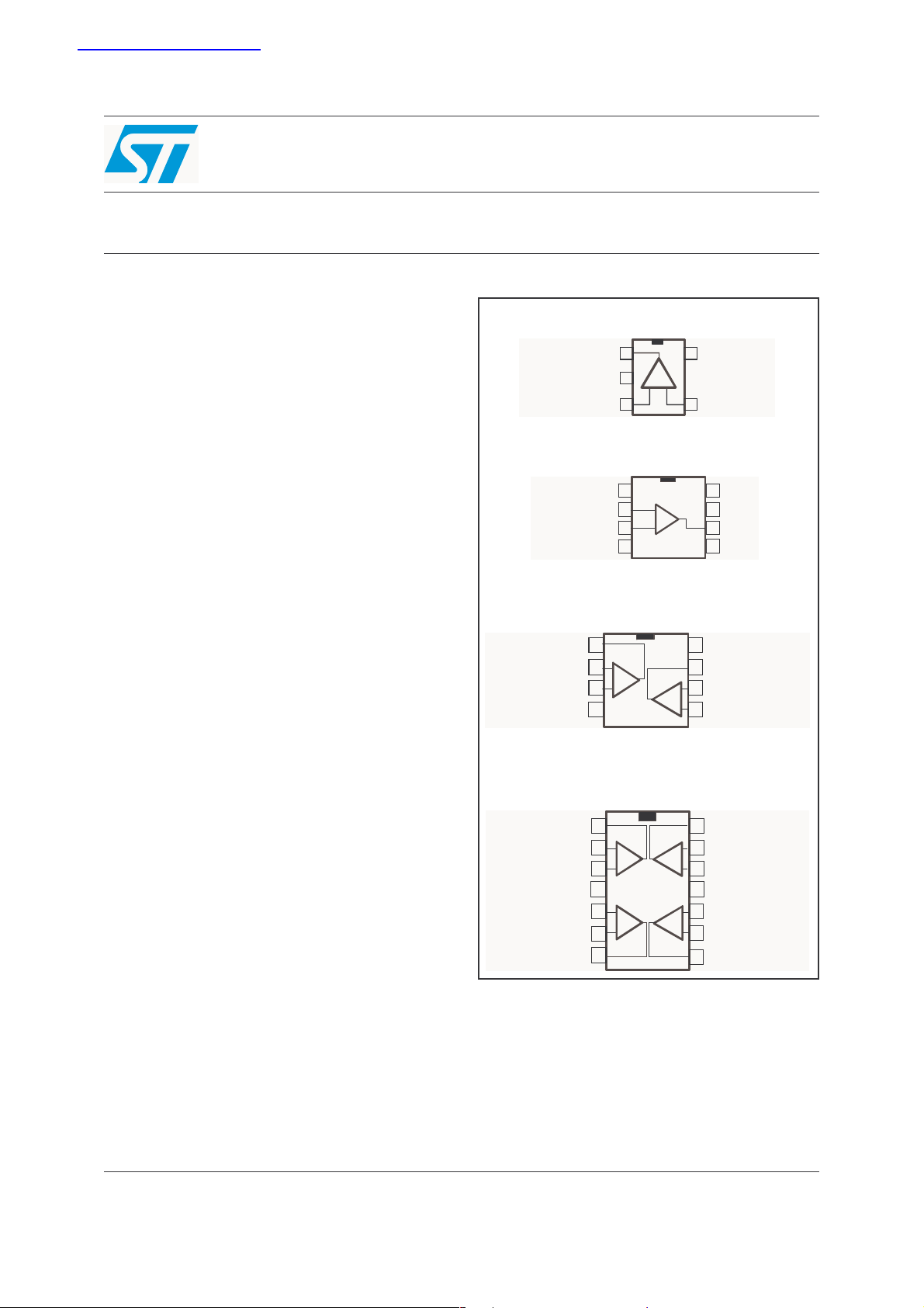
TSV321RILT
VCC
Output
Output
1
1
VDD
VDD
2
2
Non Inverting Input Inverting Input
Non Inverting Input Inverting Input
3
3
VCC
5
5
4
4
TSV321ID-TSV321IDT
N.C.
N.C.
Inverti ng Input
Inverti ng Input
Non Inver ting Input
Non Inver ting Input
VDD
VDD
1
1
_
_
2
2
+
+
3
3
8
N.C.
8
N.C.
VCC
VCC
7
7
Output
Output
6
6
N.C.
N.C.
54
54
TSV358IST-TSV358ID-TSV358IDT-TSV358IPT
Output 1
Output 1
Inverting Input 1
Inverting Input 1
Non Inverting Input 1
Non Inverting Input 1
VDD
VDD
1
1
_
_
2
2
+
+
3
3
VCC
VCC
8
8
7
7
Output 2
Output 2
_
_
Inverting Input 2
Inverting Input 2
6
6
+
+
Non Inverting Input 2
Non Inverting Input 2
54
54
TSV324ID-TSV324IDT-TSV324IPT
Output 4
Output 1
Output 1
Inverting Input 1
Inverting Input 1
Non Inverting Input 1
Non Inverting Input 1
VCC
VCC
Non Inverting Input 2
Non Inverting Input 2
Inverting Input 2
Inverting Input 2
Output 2
Output 2
1
1
_
_
2
2
+
+
3
3
4
4
5
5
+
+
_
_
6
6
7
7
Output 4
14
14
_
_
13
13
Inverting Input 4
Inverting Input 4
+
+
Non Inverting Input 4
Non Inverting Input 4
12
12
VDD
VDD
11
11
10
10
Non Inverting Input 3
Non Inverting Input 3
+
+
_
_
Inverting Input 3
Inverting Input 3
9
9
Output 3
Output 3
8
8
December 2005 Rev. 3 1/15
www.st.com
15
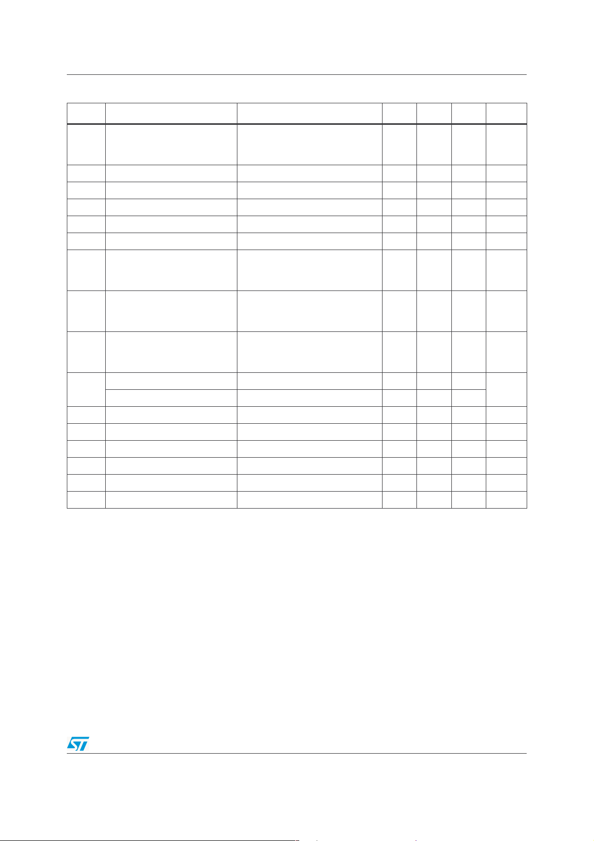
Order Codes TSV321-TSV358-TSV324
1 Order Codes
Part Number
TSV321RILT
TSV321RAILT SOT23-5L Tape & Reel K178
TSV321ID/IDT
TSV358ID/IDT V358ID
TSV358IPT
TSV358IST MiniSO-8 K175
TSV358IYD/IYDT SO-8 (automotive grade level) Tube or Tape & Reel
TSV358IYPT
TSV324ID/IDT SO-14 Tube or Tape & Reel V324ID
TSV324IPT
Temperature
Range
-40°C to +125°C
Package Packaging Marking
SOT23-5L Tape & Reel K174
SO-8 Tube or Tape & Reel
TSSOP8
(Thin Shrink Outline Package)
TSSOP8
(automotive grade level)
TSSOP14
(Thin Shrink Outline Package)
V321ID
V358I
Tape & Reel
Tape & Reel V358Y
Tape & Reel V324IP
2/15
TSV321-TSV358-TSV324 Absolute Maximum Ratings
2 Absolute Maximum Ratings
Table 1. Key parameters and their absolute maximum ratings
Symbol Parameter Value Unit
V
CC
V
id
V
T
stg
T
R
thja
ESD
Supply Voltage
Differential Input Voltage
Input Voltage VDD-0.3 to VCC +0.3
i
(1)
(2)
Storage Temperature
Maximum Junction Temperature
j
Thermal Resistance Junction to Ambient
(3)
SOT23-5
SO-8
SO-14
TSSOP8
TSSOP14
MiniSO-8
HBM: Human Body Model
MM: Machine Model
(4)
(5)
7V
±1 V
-65 to +150 °C
150 °C
250
125
103
120
100
190
2kV
200 V
CDM: Charged Device Model 1.5 kV
Latch-up Immunity 200 mA
Lead Temperature (soldering, 10s) 250 °C
Output Short Circuit Duration
see note
(6)
V
°C/W
1. All voltages values, except differential voltage are with respect to network terminal.
2. Differential voltages are the non-inverting input terminal with respect to the inverting input terminal. If Vid > ±1V, the
maximum input current must not exceed ±1mA. In this case (Vid > ±1V) an input series resistor must be added to limit input
current.
3. Short-circuits can cause excessive heating. Destructive dissipation can result from simultaneous short-circuit on all
amplifiers.
4. Human body model, 100pF discharged through a 1.5kΩ resistor into pin of device.
5. Machine model ESD, a 200pF cap is charged to the specified voltage, then discharged directly into the IC with no external
series resistor (internal resistor < 5Ω), into pin to pin of device.
6. Short-circuits from the output to VCCcan cause excessive heating. The maximum output current is approximately 80mA,
independent of the magnitude of V
. Destructive dissipation can result from simultaneous short-circuits on all amplifiers.
CC
Table 2. Operating conditions
Symbol Parameter Value Unit
V
V
V
T
1. At 25°C, for 2.5 ≤ VCC ≤ 6V, V
2. In full temperature range, both Rails can be reached when VCC does not exceed 5.5V.
Supply Voltage 2.5 to 6 V
CC
Common Mode Input Voltage Range
icm
Common Mode Input Voltage Range
icm
Operating Free Air Temperature Range -40 to + 125 °C
oper
is extended to VDD - 0.2V, VCC + 0.2V.
icm
(1)
(2)
VDD - 0.2 to VCC + 0.2 V
VDD to V
3/15
CC
V
Electrical Characteristics TSV321-TSV358-TSV324
3 Electrical Characteristics
Table 3. V
= +3V, VDD = 0V, RL, CL connected to VCC/2, T
CC
= 25°C (unless otherwise specified)
amb
Symbol Parameter Conditions Min. Typ. Max. Unit
= V
= V
V
Input Offset Voltage
V
io
icm
TSV321/358/324
TSV321A/358A/324A
∆V
Input Offset Voltage Drift 2 µV/°C
io
I
Input Offset Current
io
Input Bias Current
I
ib
(1)
1)
V
icm
V
icm
CMR Common Mode Rejection Ratio 0 ≤ V
= V
= V
icm
out
= V
out
= V
out
≤ VCC, V
/2
CC
0.2
0.1
/2 3 30 nA
CC
/2 4 125 nA
CC
= V
out
/2 60 80 dB
CC
3
1
mV
SVR Supply Voltage Rejection Ratio 70 85 dB
V
= 0.5V to 2.5V
Large Signal Voltage Gain
A
vd
V
V
High Level Output Voltage
OH
Low Level Output Voltage
OL
Output Source Current VID = 100mV, VO = V
I
o
Output Sink Current V
I
Supply Current (per amplifier) A
CC
GBP Gain Bandwidth Product R
SR Slew Rate R
φm Phase Margin C
out
= 2kΩ
R
L
R
= 600Ω
L
= 100mV
V
id
= 2kΩ
R
L
R
= 600Ω
L
= -100mV
V
id
= 2kΩ
R
L
R
= 600Ω
L
DD
= -100mV, VO = V
ID
= 1, no load 420 650 µA
VCL
= 10kΩ, CL= 100pF, f = 100kHz 1 1.3 MHz
L
= 10kΩ, CL= 100pF, AV = 1 0.42 0.6 V/µs
L
= 100pF 53 Degrees
L
CC
80
74
2.82
2.80
20 80
20 80
92
95
2.95
2.95
88
115
120
160
dB
mV
mA
en Input Voltage Noise 27 nV/√Hz
V
THD Total Harmonic Distortion 0.01 %
1. Maximum values including unavoidable inaccuracies of the industrial test.
4/15
TSV321-TSV358-TSV324 Electrical Characteristics
Table 4. VCC = +5V, VDD = 0V, RL, CL connected to VCC/2, T
= 25°C (unless otherwise specified)
amb
Symbol Parameter Conditions Min. Typ. Max. Unit
= V
= V
V
Input Offset Voltage
V
io
icm
TSV321/358/324
TSV321A/358A/324A
∆V
Input Offset Voltage Drift 2 µV/°C
io
I
Input Offset Current
io
I
Input Bias Current
ib
(1)
1)
V
icm
V
icm
CMR Common Mode Rejection Ratio 0 ≤ V
= V
= V
icm
out
= V
out
= V
out
≤ VCC, V
/2
CC
0.2
0.1
/2 3 30 nA
CC
/2 70 130 nA
CC
= V
out
/2 65 85 dB
CC
3
1
mV
SVR Supply Voltage Rejection Ratio 70 90 dB
V
= 0.5V to 2.5V
Large Signal Voltage Gain
A
vd
V
V
High Level Output Voltage
OH
Low Level Output Voltage
OL
Output Source Current VID = 100mV, VO = V
I
o
Output Sink Current V
Supply Current (per amplifier) A
I
CC
GBP Gain Bandwidth Product R
SR Slew Rate R
φm Phase Margin C
out
= 2kΩ
R
L
R
= 600Ω
L
= 100mV
V
id
= 2kΩ
R
L
R
= 600Ω
L
V
= -100mV
id
= 2kΩ
R
L
R
= 600Ω
L
DD
= -100mV, VO = V
ID
= 1, no load 500 835 µA
VCL
= 10kΩ, CL= 100pF, f = 100kHz 1 1.4 MHz
L
= 10kΩ, CL= 100pF, AV = 1 0.42 0.6 V/µs
L
= 100pF 55 Degrees
L
CC
83
77
4.80
4.75
20 80
20 80
92
85
4.95
4.90
88
115
130
188
dB
mV
mA
en Input Voltage Noise 27 nV/√Hz
V
THD Total Harmonic Distortion 0.01 %
1. Maximum values including unavoidable inaccuracies of the industrial test.
5/15

Electrical Characteristics TSV321-TSV358-TSV324
Figure 1. Supply current/amplifier vs. supply
voltage
600
600
500
500
400
400
Tamb = 25°C
300
300
200
200
Supply Current (µA)
Supply Current (µA)
100
100
0
0
02468
02468
Supply Voltage (V)
Supply Voltage (V)
Tamb = 25°C
Figure 2. Supply current/amplifier vs.
temperature
550
550
Vcc = 5V
Vcc = 5V
500
500
Vcc = 3V
450
450
400
400
350
350
Supply Current (µA)
Supply Current (µA)
300
300
250
250
-40-200 20406080100120140
-40-200 20406080100120140
Temperature (°C)
Temperature (°C)
Vcc = 3V
Figure 3. Output power vs. supply voltage Figure 4. Input offset voltage drift vs.
temperature
200
60
60
RL = 32 ohms
RL = 32 ohms
50
50
40
40
30
30
20
20
Output Power (mW)
Output Power (mW)
10
10
0
0
123456
123456
10% distortion
10% distortion
0.1% distortion
0.1% distortion
Supply Voltage (V)
Supply Voltage (V)
1% distortion
1% distortion
200
150
150
100
100
50
50
0
0
-50
-50
Input Voltage Drift (µV)
Input Voltage Drift (µV)
-100
-100
-150
-150
-40-20 0 20406080100120140
-40-20 0 20406080100120140
Temperature (°C)
Temperature (°C)
Vcc = 3V
Vcc = 3V
Vcc = 5V
Vcc = 5V
Figure 5. Input bias current vs. temperature Figure 6. Open loop gain vs. temperature
110
10.0
10.0
0.0
0.0
-10.0
-10.0
-20.0
-20.0
Input bias current (nA)
Input bias current (nA)
-30.0
-30.0
-40.0
-40.0
-40 -20 0 20 40 60 80 100 1 20 140
-40 -20 0 20 40 60 80 100 1 20 140
Temperature (°C)
Temperature (°C)
Vcc = 3V
Vcc = 3V
Vicm = 1.5V
Vicm = 1.5V
6/15
110
Vcc = 5V
Vcc = 5V
Vicm = 2.5V
Vicm = 2.5V
100
100
90
90
80
80
Open Loop Gain (dB)
Open Loop Gain (dB)
70
70
-40-20 0 20406080100120140
-40-20 0 20406080100120140
Temperature (°C)
Temperature (°C)
RL = 2 kOhms
RL = 2 kOhms
RL = 600 ohms
RL = 600 ohms

TSV321-TSV358-TSV324 Electrical Characteristics
Figure 7. Open loop gain vs. temperature Figure 8. High level output voltage vs.
temperature
110
110
Vcc = 3V
Vcc = 3V
Vicm = 1.5V
Vicm = 1.5V
100
100
90
90
80
80
Ope n Loop Gai n (dB)
Ope n Loop Gai n (dB)
70
70
-40-20 0 20406080100120140
-40-20 0 20406080100120140
Temperature (°C)
Temperature (°C)
RL = 2 kOhms
RL = 2 kOhms
RL = 600 Ohms
RL = 600 Ohms
110
110
RL = 600 ohms
RL = 600 ohms
100
100
90
90
80
80
70
70
60
60
50
50
Voltage Referenced to VCC (mV)
Voltage Referenced to VCC (mV)
40
40
-40-20 0 20 40 60 80100120140
-40-20 0 20 40 60 80100120140
Vcc = 5V
Vcc = 5V
Vcc = 3V
Vcc = 3V
Temperature (°C)
Temperature (°C)
Figure 9. Low level output voltage vs.
Figure 10. Output current vs. temperature
temperature
100
110
110
RL = 600 ohms
RL = 600 ohms
100
100
90
90
80
80
70
70
60
60
50
50
Voltage Referenced to Gnd (mV)
Voltage Referenced to Gnd (mV)
40
40
-40-20 0 20 40 60 80100120140
-40-20 0 20 40 60 80100120140
Temperature (°C)
Temperature (°C)
Vcc = 5V
Vcc = 5V
Vcc = 3V
Vcc = 3V
100
Isink
50
50
0
0
Output Current (mA)
Output Current (mA)
-50
-50
-100
-100
-40 -20 0 20 40 60 80 100 120 140
-40 -20 0 20 40 60 80 100 120 140
Isink
Vcc = 5V
Vcc = 5V
Vid = 1V
Vid = 1V
Isource
Isource
Temperature (°C)
Temperature (°C)
Figure 11. Output current vs. temperature Figure 12. Output current vs. temperature
100
100
Isink
Isink
50
50
Vcc = 3V
Vcc = 3V
Vid = 1V
0
0
Output Current (mA)
Output Current (mA)
-50
-50
Vid = 1V
Isource
Isource
100
100
50
50
0
0
T = 125 °C
T = 125 °C
Output Current (mA)
Output Current (mA)
-50
-50
T = 25 °C
T = 25 °C
T = 125 °C
T = 125 °C
T = -40 °C
T = -40 °C
Vcc = 5V
Vcc = 5V
Vid = 0.1V
Vid = 0.1V
Vicm = 2.5V
Vicm = 2.5V
sink
sink
T = 25 °C
T = 25 °C
-100
-100
-40 -20 0 20 40 60 80 100 120 140
-40 -20 0 20 40 60 80 100 120 140
Temperature (°C)
Temperature (°C)
T = -40 °C
T = -40 °C
-100
-100
0.0 1.0 2.0 3.0 4.0 5.0
0.0 1.0 2.0 3.0 4.0 5.0
Output Voltage (V)
Output Voltage (V)
source
source
7/15

Electrical Characteristics TSV321-TSV358-TSV324
Figure 13. Output current vs. temperature Figure 14. Gain & phase vs. frequency
100
100
50
50
0
0
T = 125 °C
T = 125 °C
Output Current (mA)
Output Current (mA)
-100
-100
T = 25 °C
T = 25 °C
-50
-50
T = -40 °C
T = -40 °C
0.0 0.5 1.0 1.5 2.0 2.5 3.0 3.5
0.0 0.5 1.0 1.5 2.0 2.5 3.0 3.5
T = 125 °C
T = 125 °C
T = -40 °C
T = -40 °C
Vcc = 3V
Vcc = 3V
Vid = 0.1V
Vid = 0.1V
Vicm = 1.5V
Vicm = 1.5V
Output Voltage (V)
Output Voltage (V)
sink
sink
T = 25 °C
T = 25 °C
source
source
70
70
RL = 10K
60
60
50
50
40
40
gain
gain
Gain (dB)
Gain (dB)
30
30
20
20
10
10
0
0
1E+3 1E+4 1E+5 1E+6
1E+3 1E+4 1E+5 1E+6
Frequency (Hz)
Frequency (Hz)
RL = 10K
CL = 100 pF
CL = 100 pF
Vcc = 5V
Vcc = 5V
phase
phase
180
180
160
160
140
140
120
120
100
100
80
80
60
60
40
40
Phase (°)
Phase (°)
Figure 15. Gain & phase vs. frequency Figure 16. Slew rate vs. temperature
0.75
70
70
RL = 10K
60
60
50
50
40
40
gain
gain
Gain (dB)
Gain (dB)
30
30
20
20
10
10
0
0
1E+3 1E+4 1E+5 1E+6
1E+3 1E+4 1E+5 1E+6
Frequency (Hz)
Frequency (Hz)
RL = 10K
CL = 100 pF
CL = 100 pF
Vcc = 3V
Vcc = 3V
phase
phase
180
180
160
160
140
140
120
120
100
100
80
80
60
60
40
40
Phase (°)
Phase (°)
0.75
Vcc = 5V
Vcc = 5V
gain = +1
gain = +1
0.70
0.70
Vin = 2 to 3V
Vin = 2 to 3V
0.65
0.65
RL = 10kohms
RL = 10kohms
CL = 100 pF
CL = 100 pF
0.60
0.60
0.55
0.55
0.50
0.50
Slew Rate (V/µs)
Slew Rate (V/µs)
0.45
0.45
0.40
0.40
0.35
0.35
-40-20 0 20406080100120140
-40-20 0 20406080100120140
positive Slew Rate
positive Slew Rate
neg a ti ve Slew Ra te
neg a ti ve Slew Ra te
Temperature (°C)
Temperature (°C)
Figure 17. Slew rate vs. temperature Figure 18. Distortion vs. frequency
0.150
0.70
0.70
Vcc = 3V
Vcc = 3V
gain = +1
gain = +1
0.65
0.65
Vin = 1 to 2V
Vin = 1 to 2V
RL = 10kohm
RL = 10kohm
0.60
0.60
CL = 100 pF
CL = 100 pF
0.55
0.55
0.50
0.50
Slew Rate (V/µs)
Slew Rate (V/µs)
0.45
0.45
0.40
0.40
0.35
0.35
-40-200 20406080100120140
-40-200 20406080100120140
Temperature (°C)
Temperature (°C)
positive Slew Rate
positive Slew Rate
negative Slew Rate
negative Slew Rate
8/15
0.150
0.125
0.125
0.100
0.100
0.075
0.075
Distortion (%)
Distortion (%)
0.050
0.050
0.025
0.025
0.000
0.000
Vcc = 3V
Vcc = 3V
Vout = 1Vpp
Vout = 1Vpp
RL = 32 ohms
RL = 32 ohms
gain = -1
gain = -1
1E+1 1E+2 1E+3 1E+4 1E+5
1E+1 1E+2 1E+3 1E+4 1E+5
Frequency (Hz)
Frequency (Hz)

TSV321-TSV358-TSV324 Package Mechanical Data
4 Package Mechanical Data
In order to meet environmental requirements, ST offers these devices in ECOPACK®
packages. These packages have a Lead-free second level interconnect. The category of
second level interconnect is marked on the package and on the inner box label, in
compliance with JEDEC Standard JESD97. The maximum ratings related to soldering
conditions are also marked on the inner box label. ECOPACK is an ST trademark.
ECOPACK specifications are available at: www.st.com
4.1 SO-8 Package
SO-8 MECHANICAL DATA
.
DIM.
A 1.35 1.75 0.053 0.069
A1 0.10 0.25 0.04 0.010
A2 1.10 1.65 0.043 0.065
B 0.33 0.51 0.013 0.020
C 0.19 0.25 0.007 0.010
D 4.80 5.00 0.189 0.197
E 3.80 4.00 0.150 0.157
e 1.27 0.050
H 5.80 6.20 0.228 0.244
h 0.25 0.50 0.010 0.020
L 0.40 1.27 0.016 0.050
k ˚ (max.)
ddd 0.1 0.04
MIN. TYP MAX. MIN. TYP. MAX.
mm. inch
8
0016023/C
9/15

Package Mechanical Data TSV321-TSV358-TSV324
4.2 TSSOP8 Package
TSSOP8 MECHANICAL DATA
DIM.
A 1.2 0.047
A1 0.05 0.15 0.00 2 0.006
A2 0.80 1.00 1.05 0.031 0.039 0.041
b 0.19 0.30 0.007 0.012
c 0.09 0.20 0.00 4 0.008
D 2.90 3.00 3.10 0.114 0.118 0.122
E 6.20 6.40 6.60 0.244 0.252 0.260
E1 4.30 4.40 4.50 0.169 0.173 0.177
e 0.65 0.0256
K0˚ 8˚0˚ 8˚
L 0.45 0.60 0.75 0.018 0.024 0.030
L1 1 0.039
MIN. TYP MAX. MIN. TYP. MAX.
mm. inch
10/15
0079397/D

TSV321-TSV358-TSV324 Package Mechanical Data
4.3 MiniSO-8 Package
11/15

Package Mechanical Data TSV321-TSV358-TSV324
4.4 SO-14 Package
SO-14 MECHANICAL DATA
DIM.
A 1.75 0.068
a1 0.1 0.2 0.003 0.007
a2 1.65 0.064
b 0.35 0.46 0.013 0.018
b1 0.19 0.25 0.007 0.010
C 0.5 0.019
c1 45˚ (typ.)
D 8.55 8.75 0.336 0.344
E 5.8 6.2 0.228 0.244
e 1.27 0.050
e3 7.62 0.300
F 3.8 4.0 0.149 0.157
G 4.6 5.3 0.181 0.208
L 0.5 1.27 0.019 0.050
M 0.68 0.026
S˚ (max.)
MIN. TYP MAX. MIN. TYP. MAX.
mm. inch
8
12/15
PO13G

TSV321-TSV358-TSV324 Package Mechanical Data
4.5 TSSOP14 Package
TSSOP14 MECHANICAL DATA
DIM.
A 1.2 0.047
A1 0.05 0.15 0.002 0.004 0.006
A2 0.8 1 1.05 0.031 0.039 0.041
b 0.19 0.30 0.007 0.012
c 0.09 0.20 0.004 0.0089
D 4.9 5 5.1 0.193 0.197 0.201
E 6.2 6.4 6.6 0.244 0.252 0.260
E1 4.3 4.4 4.48 0.169 0.173 0.176
e 0.65 BSC 0.0256 BSC
K0˚ 8˚0˚ 8˚
L 0.45 0.60 0.75 0.018 0.024 0.030
MIN. TYP MAX. MIN. TYP. MAX.
A2
A
A1
mm. inch
b
e
c
K
L
E
PIN 1 IDENTIFICATION
D
E1
1
0080337D
13/15

Package Mechanical Data TSV321-TSV358-TSV324
4.6 SOT23-5 Package
SOT23-5L MECHANICAL DATA
DIM.
A 0.90 1.45 35.4 57.1
A1 0.00 0.15 0.0 5.9
A2 0.90 1.30 35.4 51.2
b 0.35 0.50 13.7 19.7
C 0.09 0.20 3.5 7.8
D 2.80 3.00 110.2 118.1
E 2.60 3.00 102.3 118.1
E1 1.50 1.75 59.0 68.8
e.95 37.4
e1 1.9 74.8
L 0.35 0.55 13.7 21.6
MIN. TYP MAX. MIN. TYP. MAX.
mm. mils
0
14/15

TSV321-TSV358-TSV324 Revision History
5 Revision History
Table 5. Document revision history
Date Revision Changes
Aug. 2005 1 – First Release - Products in full production
– Addition of TS321A/TS324A/TS358A data in tables in
Sept. 2005 2
Chapter 3: Electrical Characteristics on page 4
– Minor formatting and grammatical changes.
.
Dec. 2005 3
– Missing PPAP references inserted see
on page 2
.
Table 1: Order Codes
Information furnished is believed to be accurate and reliable. However, STMicroelectronics assumes no responsibility for the consequences
of use of such information nor for any infringement of patents or other rights of third parties which may result from its use. No license is
granted by implication or otherwise under any patent or patent rights of STMicroelectronics. Specifications mentioned in this publication are
subject to change without notice. This publication supersedes and replaces all information previously supplied. STMicroelectronics products
are not authorized for use as critical components in life support devices or systems without express written approval of STMicroelectronics.
The ST logo is a registered trademark of STMicroelectronics.
All other names are the property of their respective owners
© 7 STMicroelectronics - All rights reserved
STMicroelectronics group of companies
Australia - Belgium - Brazil - Canada - China - Czech Republic - Finland - France - Germany - Hong Kong - India - Israel - Italy - Japan -
Malaysia - Malta - Morocco - Singapore - Spain - Sweden - Switzerland - United Kingdom - United States of America
www.st.com
15/15
 Loading...