

TSM103W
Dual O p erat io na l A mpl i fie r an d Voltage R efe re nce
OPERATIONAL AMPLIFIER
■ LOW INP UT OFFSET V OLTAGE : 0.5mV
typ.
■ LOW SUPPLY CURRENT : 350µA/op.
(@ V
= 5V)
CC
■ MEDIUM BANDWIDTH (unity gain) : 0.9MHz
■ LARGE OUTPUT VOLTAGE SWING : 0V to
(V
- 1.5V)
CC
■ INPUT COMMON MODE VOLTAGE RANGE
INCLUDES GROUND
■ WIDE POWER SUPPLY RANGE : 3 to 32V
±1.5 T O ±16V
■ 1.5kV ESD PROTECTION
■ VOLTAGE REFERENCE
■ FIXED OUTPUT VOLTAGE REFERENCE
2.5V
■ ±0.4% OR ±0.7% V O LTAGE PRECISION
■ SINK CURRENT CAPABILITY : 1 to 100mA
■ TYPICAL OUTPUT IMPEDANCE : 0.2Ω
DESCRIPTION
The TSM103W is a monolithic IC that includes
one independent op-amp and another op-amp for
which the non-inverting input is wired to a 2.5V
fixed Voltage Reference. T his device offers both
space and cost savings in many applications such
as power supply m anagemen t or data acqui sition
systems.
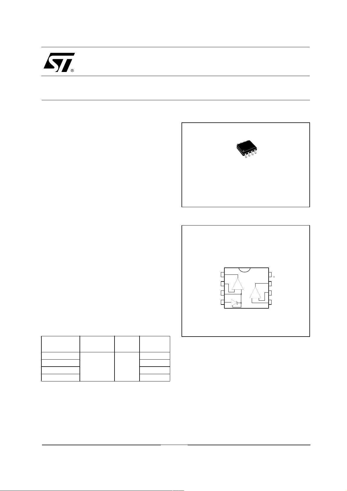
D
SO-8
(Plastic Micropackage)
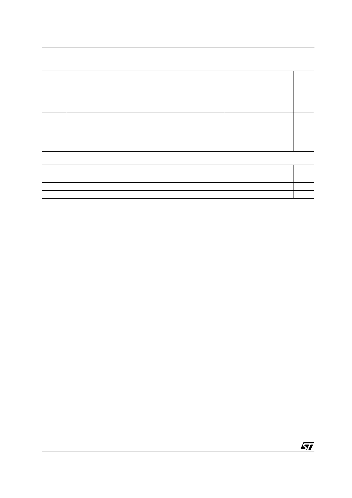
PIN C ONNECTIONS (top view)
Output 1
Inverting Input 1
Non-inverting Input 1
V
-
CC
1
2
3
4
OP1
OP2
-
+
+
-
VRef
V
8
CC
Output 2
7
Inverting Input 2
6
Non-inverting Input 2
5
+
ORDER CODE
Part Number
TSM103WID
TSM103WIDT Tape & Ree
TSM103WAID Tube
TSM103WAIDT Tape & Reel
April 2004 1/7
Temperature
Range
Package Packaging
-40, +105°C SO-8
Tube
Revision 3
TSM103W ABSOLUTE MAXIMUM RATINGS
1 ABSOLUTE MAXIMUM RATINGS
Symbol Parameter Value Unit
V
T
Supply Voltage
CC
Differential Input Voltage
V
id
Input VoltageL
V
i
Storage temperatur e range
stg
36 V
Vcc + 0.6 V
-0.3 to Vcc + 0.3V V
-65 to + 150 °C
Ik Continuous cathode current range -100 to 150 mA
Maximum Junction Temperature
T
j
R
Thermal Resistance Junction to Ambient (SO package)
thja
Maximum Lead Temperature (10 seconds maximum)
T
l
150 °C
175 °C/W
260 °C
ESD Electrostatic Discharge Protection 1.5 kV
OPERATING CONDITIONS
Symbol Parameter Value Unit
Vcc DC Supply Conditions 3 to 32 V
I
Vref Cathode Current
k
T
Operating Free-air Temperature Range
oper
1 to 100 mA
-40°C, +105°C °C
2/7
ELECTRICAL CHARACTERISTICS TSM103W
2 ELECTRICAL CHARACTERISTICS
Symbol Parameter Min. Typ. Max. Unit
Total Supply Current, excluding Current in the
Voltage Reference
I
CC
Vcc+ = 5V, no load
Tmin. < Tamb < Tmax.
Vcc+ = 30V, no load
0.7 1.2
2
mA
Tmin. < Tamb < Tmax
OPERATOR 2 (independent op-amp)
+
V
= +5V, VCC = Ground, Vo = 1.4V,T
CC
Symbol Parameter Min. Typ. Max. Unit
Input Offset Voltage
V
= 0V
icm
V
DV
TSM103WA, T
io
T
≤ T
min.
amb
TSM103W, T
T
≤ T
min.
amb
Input Offset Voltage Drift
io
I
io
I
ib
Input Offset Current
T
≤ T
min.
amb
Input Bias Current
T
≤ T
min.
amb
≤ T
≤ T
≤ T
≤ T
amb
amb
max.
= 25°
max.
max.
max
= 25°
Large Signal Voltage Gain
V
Avd
SVR
= 15V, RL = 2k, Vo = 1.4V to 11.4V
CC
T
≤ T
amb
≤ T
max.
min.
Supply Voltage Rejection Ratio
V
= 5V to 30V
CC
Input Common Mode Voltage Range
Vicm
CMR
I
source
I
o
V
= +30V - see note
CC
T
≤ T
amb
≤ T
max.
min.
Common Mode Rejection Ratio
T
≤ T
amb
≤ T
max.
min.
Output Current Source
V
= +15V, Vo = 2V, Vid = +1V
CC
Short Circuit to Ground
V
= +15V
CC
1
Output Current Sink
V
= -1V,
I
sink
id
V
= +15V, Vo = 2V
CC
V
= +15V, Vo = 0.2V
CC
High Level Output Voltage
+
V
= 30V
CC
T
= 25°C, RL = 2k
V
OH
amb
T
≤ T
min.
T
amb
T
min.
≤ T
amb
= 25°C, RL = 10k
≤ T
≤ T
amb
max
max.
Low Level Output Voltage
R
V
OL
L
T
min.
= 10k
≤ T
amb
≤ T
max.
Slew Rate at Unity Gain
= 0.5 to 3V, VCC = 15V
SR
V
i
R
= 2k, CL = 100pF, unity gain
L
= 25°C (unless otherwise specified)
amb
50
25
65 100 dB
0
0
70
60
20 40 mA
10
12
26
26
27
27
0.2 0.4
0.5
1
2
3
4
mV
5
7
2
75
150
20 150
200
µV/°C
nA
nA
100 V/mV
+) -1.5
(V
85
(V
CC
CC
+
) -2
V
dB
40 60 mA
20
50
mA
µA
27
28
520
20
V
mV
V/µs
3/7

TSM103W ELECTRICAL CHARACTERISTICS
Symbol Parameter Min. Typ. Max. Unit
Gain Bandwidth Product
= 30V,RL = 2k, CL = 100pF
GBP
V
CC
f = 100kHz, V
= 10mV
in
0.5 0.9
MHz
Total Harmonic Distortion
THD
f = 1kHz
= 20dB,RL = 2k, VCC = 30V
A
V
C
= 100pF, Vo = 2V
L
pp
0.02
%
Equivalent Input Noise Voltage
e
1) The input common-mode vol t age of eit her input signal vol t age should not be allowed to go negative by more than 0.3V. T he upper end
of the common-mode voltage range is V
f = 1kHz, Rs = 100
n
Vcc = 30V
Ω
+
- 1.5V. Both inputs can go to Vcc+ 0.3V without damage.
CC
50 nV/
√Hz
OPERATOR 1 (op-amp with non-inverting input connected to the internal Vref)
+
V
= +5V, V
CC
Symbol Parameter Min. Typ. Max. Unit
V
io
DV
io
I
ib
Avd
SVR
I
source
I
o
I
sink
V
OH
V
OL
SR
-
= Ground, T
CC
= 25°C (unless otherwise specified)
amb
Input Offset Voltage
= 0V
V
icm
TSM103WA, T
T
≤ T
min.
amb
TSM103W, T
T
≤ T
min.
amb
Input Offset Voltage Drift
≤ T
≤ T
amb
amb
max.
= 25°
max.
= 25°
0.5
1
7
2
3
4
mV
5
µV/°C
Input Bias Current
negative input 20 nA
Large Signal Voltage Gain
= 15V, RL = 2k, Vo = 1.4V to 11.4V
V
CC
T
≤ T
min.
amb
≤ T
max
100 V/mV
Supply Voltage Rejection Ratio
V
= 0V
icm
+
V
= 5V to 30V
CC
65 100 dB
Output Current Source
V
= 2V
o
V
= +15V, Vid = +1V 20 40 mA
CC
Short Circuit to Ground
V
= +15V
CC
40 60 mA
Output Current Sink
V
= -1V,
id
V
= +15V, Vo = 2V
CC
V
= +15V, Vo = 0.2V
CC
10
12
20
50
mA
µA
High Level Output Voltage
+
V
= 30V
CC
T
= 25°C, RL = 2k
amb
T
≤ T
min.
T
amb
T
min.
≤ T
amb
= 25°C, RL = 10k
≤ T
≤ T
amb
max.
max.
26
26
27
27
27
V
28
Low Level Output Voltage
R
L
T
min.
= 10k
≤ T
amb
≤ T
max.
520
20
mV
Slew Rate at Unity Gain
= 0.5 to 2V, VCC = 15V
V
i
R
= 2k, CL = 100pF, unity gain
L
0.2 0.4
V/µs
4/7

ELECTRICAL CHARACTERISTICS TSM103W
Symbol Parameter Min. Typ. Max. Unit
Gain Bandwidth Product
= 30V,RL = 2k, CL = 100pF
GBP
V
CC
f = 100kHz, V
= 10mV
in
0.5 0.9
MHz
Total Harmonic Distortion
THD
f = 1kHz
= 20dB,RL = 2k, VCC = 30V
A
V
C
= 100pF, Vo = 2V
L
pp
0.02
%
VOLTAGE REFERENCE
Symbol Parameter Min. Typ. Max. Unit
Reference Input Voltage, Ik=10mA
TSM103WA
T
V
ref
min.
≤ T
TSM103W ±0.7% T
T
≤ T
min.
Reference Input Voltage Deviation Over T emperature
∆V
I
min
|Z
KA
1) The dyna m i c im pedance is def i ned as [ZKA| = ∆VKA/∆I
Range
ref
V
= V
KA
T
≤ T
min.
Minimum Cathode Current for Regulation
V
= V
KA
Dynamic Impedance - note
|
VKA = V
±0.4% T
≤ T
amb
max.
≤ T
amb
max.
; Ik = 10mA
ref
≤ T
amb
max.
ref
, ∆IK = 1 to 100mA, f < 1kHz
ref
amb
amb
= 25°C
= 25°C
1
2.49
2.48
2.482
2.465
2.5
2.500
7
2.51
2.52
2.518
2.535
30
V
mV
0.5 1 mA
0.2 0.5
K
Ω
5/7

TSM103W ELECTRICAL CHARACTERISTICS
PACKAGE MECHANICAL DATA
SO-8 MECHANICAL DATA
DIM.
A 1.35 1.75 0.053 0.069
A1 0.10 0.25 0.04 0.010
A2 1.10 1.65 0.043 0.065
B 0.33 0.51 0.013 0.020
C 0.19 0.25 0.007 0.010
D 4.80 5.00 0.189 0.197
E 3.80 4.00 0.150 0.157
e 1.27 0.050
H 5.80 6.20 0.228 0.244
h 0.25 0.50 0.010 0.020
L 0.40 1.27 0.016 0.050
k ˚ (max.)
ddd 0.1 0.04
MIN. TYP MAX. MIN. TYP. MAX.
mm. inch
8
6/7
0016023/C

SUMMARY OF CHANGES TSM103W
3 SUMMARY OF CHANGES
Date Revision Description of Changes
1-2 First Release
1 - Vid=Vcc+0.6 modified on AMR table - page 2
02-April-2004 3
2 - Add Ik parameter on AMR table - page 2
3 - Avd test condition equal on both tables Operator 1 & Operator 2 pages 3 & 4
Information furnished is believed to be accurate and reliable. However, STMicroelectronics a ssumes no responsibility for the
consequences of use of such information nor for any infringement of patents or other rights of third parties which may result from
its use. No license i s granted by implication or otherwise under any pat ent or patent rights of STMi croe lectronics. Specifications
mentioned in this publication are subject to change without notice. This publicatio n supersedes and replaces all information
previously supplied. STMicroe lectronics products are not aut horized for use as cr itical components in life su pport devices or
systems without express written approval of STMicroelectronics.
The ST logo is a registered trademark of STMicroelectronics
All other n ames are the property of their respecti ve owners
© 2004 STMicroelectronics - All Rights Reserved
Australi a - Belgium - B raz il - Canada - China - Czech Repubic - Finl and - France - Germany - Hong Kong - India - Is rael - Italy - Japan
Malaysia - M al ta - Morocco - Singapore - Spain - Sweden - Sw i tzerland - United Kingdom - United States
STMicroelectronics GROUP OF COMPANIES
www.st.com
7/7
 Loading...