

Hi-fi stereo/mono infrared transmitter
Features
■ Supply voltage: 2.3 to 5.5 V
■ Carrier frequency range: 0.4 to 11 MHz
■ High versatility: I/O pins for each section
■ Two FM transmitters for stereo
■ Sinusoidal carriers for high spectral purity
■ Micro- or line-level preamplifiers with ALC
■ VOX function to save on battery power
■ Transmitter TX2 standby for mono operation
Applications
■ Infrared hi-fi stereo transmitters
■ Infrared headsets
■ Stereo sub-carriers for video transmitters
■ Voice-operated wireless webcams
■ FM IF transmit systems
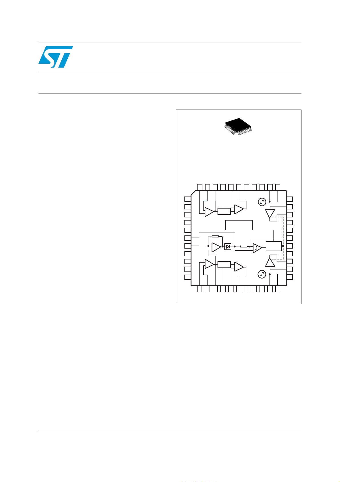
Description
The TSH512 is a 0.4- to 11-MHz dual FM
transmitter. Access pins to each section give high
versatility and allow for several different
applications: stereo headphone, multimedia
headset, audio sub-carrier generator.
The TSH512 integrates in a single chip low-noise
audio preamplifiers with ALC (automatic level
control), frequency-modulated oscillators, and
linear output buffers to drive the external
transistors. The sinusoidal carriers facilitate the
filtering and allow high performance audio
transmission.
TSH512
and stereo sub-carrier generator
F
TQFP44
10 x 10 mm
Pin connections (top view)
36
36
Monostable
Monostable
3435
3435
33
33
32
32
31
31
30
30
29
29
28
28
27
27
26
26
25
25
24
24
23
23
3738394041
PEA
PEA
-
+
+
-
-+-
VOX
VOX
PEA
PEA
TX2
TX2
TX1
TX1
3738394041
VCO
VCO
VCO
VCO
Output
Output
buffer
buffer
Output
Output
buffer
buffer
424344
424344
1
1
2
2
3
3
4
4
5
5
6
6
7
7
8
8
9
9
10
10
11
11
-
+
ALC
ALC
LNA
LNA
TSH512
TSH512
-
-
+
+
LNA
LNA
+
ALC
ALC
-+
--+
12 13 14 15 16 17 18 19 20 21 22
12 13 14 15 16 17 18 19 20 21 22
The TSH512 forms a chipset with the dual
receiver TSH511.
The VOX (voice operated transmit) circuitry
disables the output buffer when there is no audio
signal to save battery power. For MONO
applications, the STANDBY pin enables one
transmitter only, reducing the supply current.
May 2009 Doc ID 8120 Rev 7 1/31
www.st.com
31

Contents TSH512
Contents
1 Absolute maximum ratings and operating conditions . . . . . . . . . . . . . 3
2 Device diagrams and schematics . . . . . . . . . . . . . . . . . . . . . . . . . . . . . . 4
3 Electrical characteristics . . . . . . . . . . . . . . . . . . . . . . . . . . . . . . . . . . . . . 7
3.1 Supply section . . . . . . . . . . . . . . . . . . . . . . . . . . . . . . . . . . . . . . . . . . . . . 10
3.2 Audio section . . . . . . . . . . . . . . . . . . . . . . . . . . . . . . . . . . . . . . . . . . . . . . 10
3.3 RF section . . . . . . . . . . . . . . . . . . . . . . . . . . . . . . . . . . . . . . . . . . . . . . . . 13
4 Application information . . . . . . . . . . . . . . . . . . . . . . . . . . . . . . . . . . . . . 14
4.1 Infrared stereo transmitter application (stereo headphones) . . . . . . . . . . 14
4.2 Sub-carrier generator application: voice-operated wireless camera . . . . 16
4.3 Multimedia application . . . . . . . . . . . . . . . . . . . . . . . . . . . . . . . . . . . . . . . 16
4.3.1 Headset side . . . . . . . . . . . . . . . . . . . . . . . . . . . . . . . . . . . . . . . . . . . . . 16
4.3.2 Computer side . . . . . . . . . . . . . . . . . . . . . . . . . . . . . . . . . . . . . . . . . . . . 17
5 General description . . . . . . . . . . . . . . . . . . . . . . . . . . . . . . . . . . . . . . . . . 18
5.1 LNA section: low noise amplifier . . . . . . . . . . . . . . . . . . . . . . . . . . . . . . . 18
5.2 Electret condenser microphone source . . . . . . . . . . . . . . . . . . . . . . . . . . 19
5.3 MIC-BIAS section: microphone bias voltage . . . . . . . . . . . . . . . . . . . . . . 20
5.4 ALC section: automatic level control . . . . . . . . . . . . . . . . . . . . . . . . . . . . 21
5.5 VOX description: voice operated transmit . . . . . . . . . . . . . . . . . . . . . . . . 21
5.6 PEA section: pre-emphasis . . . . . . . . . . . . . . . . . . . . . . . . . . . . . . . . . . . 24
5.7 VCO section: voltage-controlled oscillator . . . . . . . . . . . . . . . . . . . . . . . . 25
5.8 Output buffer section . . . . . . . . . . . . . . . . . . . . . . . . . . . . . . . . . . . . . . . . 26
5.9 SBY pin: standby for mono operation . . . . . . . . . . . . . . . . . . . . . . . . . . . . 26
6 Package information . . . . . . . . . . . . . . . . . . . . . . . . . . . . . . . . . . . . . . . . 27
6.1 TQFP44 package information . . . . . . . . . . . . . . . . . . . . . . . . . . . . . . . . . 28
7 Ordering information . . . . . . . . . . . . . . . . . . . . . . . . . . . . . . . . . . . . . . . 29
8 Revision history . . . . . . . . . . . . . . . . . . . . . . . . . . . . . . . . . . . . . . . . . . . 30
2/31 Doc ID 8120 Rev 7
TSH512 Absolute maximum ratings and operating conditions
1 Absolute maximum ratings and operating conditions
Table 1. Absolute maximum ratings
Symbol Parameter Value Unit
V
CC
T
oper
T
stg
T
j
R
thjc
R
thja
Latch-up Class
Supply voltage
Operating free air temperature range -40 to +85 °C
Storage temperature -65 to +150 °C
Maximum junction temperature 150 °C
Thermal resistance junction to case 14 °C/W
Thermal resistance junction to ambient area 45 °C/W
(2)
ESD sensitive device: handling precautions required
ESD
except pins 20 and
36
1. All voltage values, except differential voltage, are with respect to network ground terminal.
2. Corporate ST Microelectronics procedure number 0018695.
3. Human body model: a 100 pF capacitor is charged to the specified voltage, then discharged through a
1.5 kΩ resistor between two pins of the device. This is done for all couples of connected pin combinations
while the other pins are floating.
4. Charged device model: all pins and the package are charged together to the specified voltage and then
discharged directly to the ground through only one pin. This is done for all pins.
5. Machine model: a 200 pF capacitor is charged to the specified voltage, then discharged directly between
two pins of the device with no external series resistor (internal resistor < 5 Ω). This is done for all couples of
connected pin combinations while the other pins are floating.
HBM: human body model
CDM: charged device model
MM: machine model
(1)
(5)
(3)
(4)
7V
A
2
1
kV
0.2
Table 2. Operating conditions
Symbol Parameter Value Unit
V
CC
f
audio
f
carrier
Supply voltage 2.3 to 5.5 V
Audio frequency range 20 to 20,000 Hz
Carrier frequency range 0.4 to 11 MHz
Doc ID 8120 Rev 7 3/31
Device diagrams and schematics TSH512
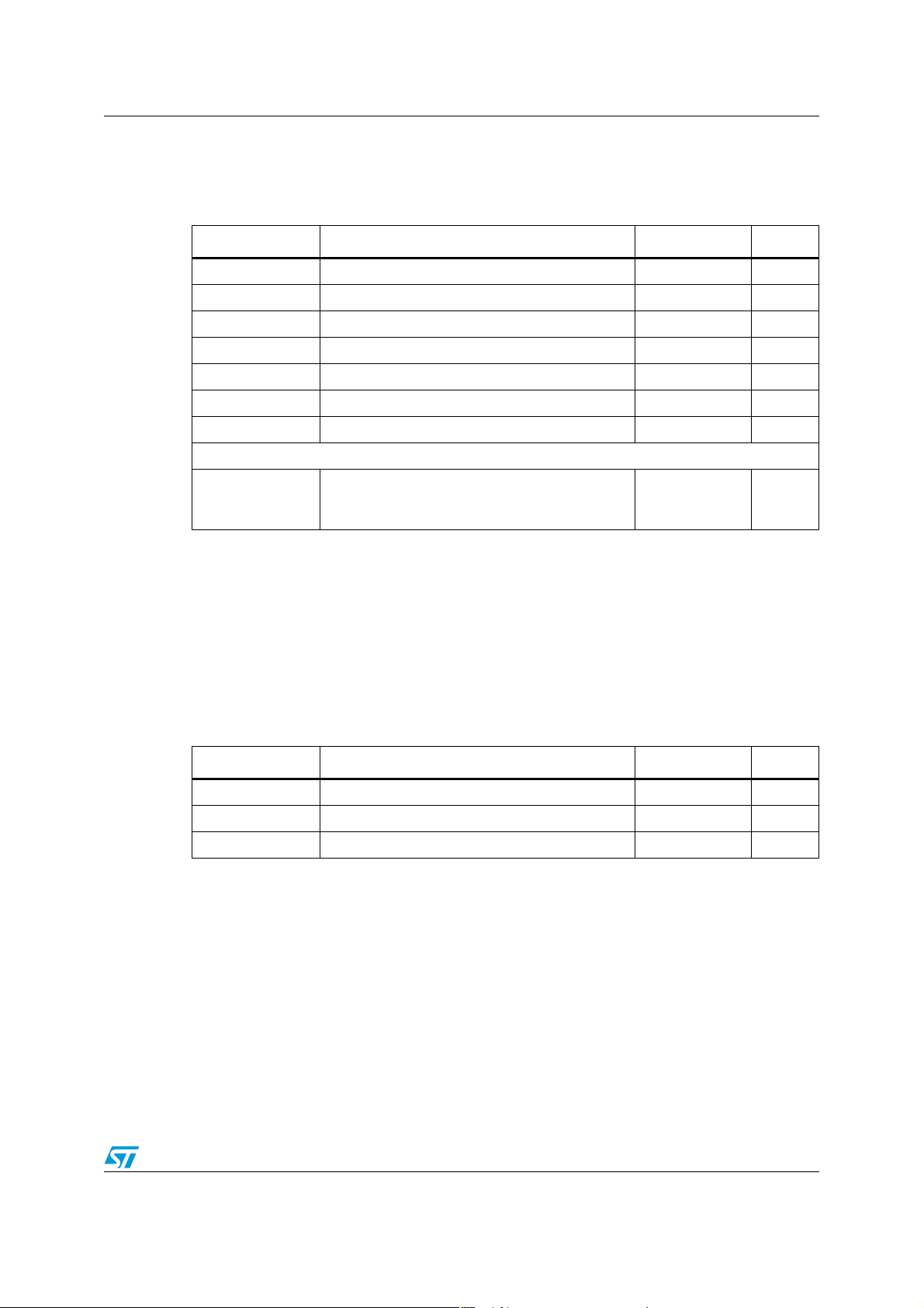
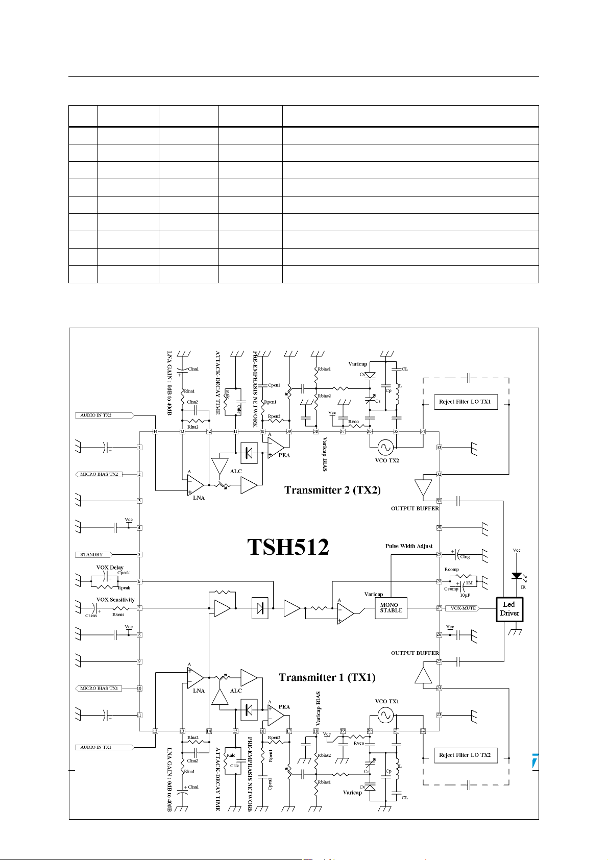
2 Device diagrams and schematics
This section contains a detailed block diagram of the TSH512 (Figure 1), with an
accompanying pin description (Table 3 on page 5), as well as the schematics of a typical
application (Figure 2 on page 6).
Figure 1. Block diagram
DEC2
DEC2
MIC-BIAS2
MIC-BIAS2
GND
GND
VCC
VCC
SBY
SBY
VOX-INTS
VOX-INTS
VOX-SENS
VOX-SENS
VCC
VCC
GND
GND
MIC-BIAS1
MIC-BIAS1
DEC1
DEC1
VCO-BIAS2
LNA-INP2
LNA-INP2
1
1
2
2
3
3
LNA
LNA
4
4
5
5
6
6
7
7
8
8
LNA
LNA
9
9
10
10
11
11
12 13 14 15 16 17 18 19 20 21 22
12 13 14 15 16 17 18 19 20 21 22
LNA-OUT2
ALC-INT2
LNA-OUT2
LNA-INN 2
LNA-INN 2
-
+
+
-+
--+
ALC-INT2
PEA-INN2
PEA-INN2
424344
424344
ALC
ALC
TSH512
TSH512
-
-
+
+
ALC
ALC
PEA-OUT2
PEA-OUT2
PEA
PEA
-
+
+
VOX
VOX
-
-+-
PEA
PEA
VCO-BIAS2
TX2
TX2
TX1
TX1
3738394041
3738394041
VCO
VCO
VCO
VCO
VCC
VCC
VCO-A2
VCO-A2
36
36
Output
Output
buffer
buffer
Output
Output
buffer
buffer
Monostable
Monostable
VCO-OUT2
VCO-OUT2
VCO-B2
VCO-B2
3435
3435
33
33
GND
GND
32
32
BUF-IN2
BUF-IN2
31
31
BUF-OUT2
BUF-OUT2
30
30
GND
GND
29
29
VOX-TIMER
VOX-TIMER
28
28
VOX-INTN
VOX-INTN
27
27
VOX-MUTE
VOX-MUTE
26
26
VCC
VCC
25
25
BUF-OUT1
BUF-OUT1
BUF-IN1
BUF-IN1
24
24
23
23
GND
GND
LNA-INP1
LNA-INP1
LNA-INN 1
LNA-INN 1
LNA-OUT1
LNA-OUT1
4/31 Doc ID 8120 Rev 7
VCC
VCC
VCO-A1
VCO-B1
VCO-A1
ALC-INT1
PEA-INN1
ALC-INT1
PEA-INN1
PEA-OUT1
PEA-OUT1
VCO-BIAS1
VCO-BIAS1
VCO-B1
VCO-OUT1
VCO-OUT1
TSH512 Device diagrams and schematics
Table 3. Pin descriptions
Pin Pin name Related to Direction
(1)
Pin description
1 DEC2 TX2 - Decoupling capacitor for internal voltage reference
2 MIC-BIAS2 TX2 O Microphone bias
3 GND - - Ground
4 VCC - - Supply voltage
5 SBY TX1 & TX2 I Standby control (input pin)
6 VOX-INTS TX1 & TX2 - Time constant terminal for audio signal integrator in VOX
7 VOX-SENS TX1 & TX2 - Gain adjustment for VOX input sensitivity
8 VCC - - Supply voltage
9 GND - - Ground
10 MIC-BIAS1 TX1 O Microphone bias
11 DEC1 TX1 - Decoupling capacitor for internal voltage reference
12 LNA-INP1 TX1 I LNA positive input
13 LNA-INN1 TX1 I LNA negative input
14 LNA-OUT1 TX1 O LNA output
15 ALC-INT1 TX1 - Time constant terminal for integrator in ALC
16 PEA-INN1 TX1 I Pre-emphasis amplifier negative input
17 PEA-OUT1 TX1 O Pre-emphasis amplifier output
18 VCO-BIAS1 TX1 O Bias for external VCO components
19 VCC - - Supply voltage
20 VCO-A1 TX1 - Oscillator component connection
21 VCO-B1 TX1 - Oscillator component connection
22 VCO-OUT1 TX1 O VCO output
23 GND - - Ground
24 BUF-IN1 TX1 I Input to the output buffer
25 BUF-OUT1 TX1 O Output of the output buffer
26 VCC - - Supply voltage
27 VOX-MUTE TX1 & TX2 O Mute control (output pin) in VOX
28 VOX-INTN TX1 & TX2 - Time constant terminal for noise integrator in VOX
29 VOX-TIMER TX1 & TX2 - Rise time for timer in VOX
30 GND - - Ground
31 BUF-OUT2 TX2 O Output of the output buffer
32 BUF-IN2 TX2 I Input to the output buffer
33 GND - - Ground
34 VCO-OUT2 TX2 O VCO output
35 VCO-B2 TX2 - Oscillator component connection
Doc ID 8120 Rev 7 5/31
Device diagrams and schematics TSH512
Table 3. Pin descriptions (continued)
Pin Pin name Related to Direction
36 VCO-A2 TX2 - Oscillator component connection
37 VCC - - Supply voltage
38 VCO-BIAS2 TX2 O Bias for external VCO components
39 PEA-OUT2 TX2 O Pre-emphasis amplifier output
40 PEA-INN2 TX2 I Pre-emphasis amplifier negative input
41 ALC-INT2 TX2 - Time constant terminal for internal peak detector in ALC
42 LNA-OUT2 TX2 O LNA output
43 LNA-INN2 TX2 I LNA negative input
44 LNA-INP2 TX2 I LNA positive input
1. Pin directions: I = input pin, O = output pin, - = pin to connect to supply or decoupling capacitors or external components.
(1)
Pin description
Figure 2. Typical application schematics for stereo infrared transmitter
6/31 Doc ID 8120 Rev 7
TSH512 Electrical characteristics
3 Electrical characteristics
Table 4. Electrical characteristics for VCC = 2.7 V, T
(unless otherwise specified)
(1)
= 25° C, f
amb
audio
= 1 kHz, f
carrier
= 2.8 MHz
Symbol Parameter Test conditions Min. Typ. Max. Unit
Overall circuit
TX1 on, TX2 on, MIC-BIAS1 and
MIC-BIAS2 not used:
I
CC_TOT
Current consumption
TX1 and TX2 are on
VOX-MUTE=1 output buffers on
VOX-MUTE=0, output buffers off
-40° C < T
<+85°C
amb
VOX-MUTE=1 output buffers on
VOX-MUTE=0, output buffers off
161118.6
12.8
19.6
13.8
TX1 on, TX2 off, MIC-BIAS1 and
MIC-BIAS2 not used:
I
CC_SBY
Current consumption with
TX2 in standby: SBY (pin5)
active
VOX-MUTE=1,output buffers on
VOX-MUTE=0, output buffers off
-40° C < T
<+85°C
amb
VOX-MUTE=1, output buffers on
VOX-MUTE=0, output buffers off
10711.5
8
12.1
8.6
LNA sections (for TX1 and TX2)
GBP
Gain bandwidth product No external load 7 MHz
LNA
Input resistance on positive
Rin
LNA
input:
(LNA-INP1 pin 12 or
30 kΩ
LNA-INP2 pin 44)
THD
En
Total harmonic distortion
LNA
Equivalent input noise
voltage
=0dB, Vout
LNA
-40° C < T
G
LNA
R
S
amb
=40dB, at f=1kHz
=390Ω, R
< +85° C 0.05
feedback
LNA
= 700 mV
=39kΩ
PP
0.01 0.05
6nV/√Hz
G
Automatic level control (ALC) section
G
ALC
V
ALC_OUT
Voltage gain 20 dB
Regulated output level
600 710 800
(at positive input of the PEA
amplifier)
-40° C < T
< +85° C 597 803
amb
Pre-emphasis amplifier (PEA) section
mA
mA
%
mVpp
Gain bandwidth product
GBP
(PEA-OUT1 pin 17 or
PEA
No load 9 MHz
PEA-OUT2 pin 39)
V
Opp-PEA
Output voltage RL = 22 kΩ 550 mVpp
Doc ID 8120 Rev 7 7/31
Electrical characteristics TSH512
Table 4. Electrical characteristics for VCC = 2.7 V, T
(unless otherwise specified) (continued)
(1)
amb
= 25° C, f
audio
= 1 kHz, f
carrier
= 2.8 MHz
Symbol Parameter Test conditions Min. Typ. Max. Unit
Audio LNA+ALC+PEA sections
G
= 0 dB, f = 1 kHz
LNA
(V
in)ALC
< 25 mV
(-30 dBu)
rms
RL = 22 kΩ tied to GND
0.05 0.15
THD
Total harmonic distortion in
linear region on PEA-OUT1
ALC
pin17 or PEA-OUT2 pin 39
< +85° C 0.25
amb
= 36 mV
= 100 mV
amb
= 36 mV
= 100 mV
(-27 dBu)
rms
(-18 dBu)
rms
<+85°C
(-27 dBu)
rms
(-18 dBu)
rms
1.331.7
4
2.5
5.3
70 °
THD
ΦΜ
AGC
PEA
Total harmonic distortion in
compression region
Phase margin at
PEA-OUT1 pin 17 or
PEA-OUT2 pin 39
-40° C < T
(V
in)ALC
(Vin)
ALC
= 22 kΩ tied to GND
R
L
-40° C < T
(V
in)ALC
(Vin)
ALC
=22kΩ
R
L
LNA and PEA at unity gain
= 40 mV
V
in
Microphone biasing section
V
MIC-BIAS
Microphone biasing voltage
(Section 5.3 on page 20)
I
MIC-BIAS
-40° C < T
= 2.5 mA 2.15 2.25 2.35
< +85° C 2.14 2.36
amb
Over temp. range:
ΔV
I
MIC-BIAS
PSRR
MIC-BIAS
MIC-BIAS
V
MIC-BIAS
coefficient
MIC-BIAS current capability Over VCC range [2.3 V–5.5 V] 2.5 mA
Power supply rejection ratio
of MIC-BIAS
temperature
[0, 70° C]
[-40, 85° C]
I
MIC-BIAS
= 2.5 mA
At 1 kHz and V
ripple
= 25 mV
RMS
260
460
50 dB
%
%
V
ppm/°C
en
MIC-BIAS
Equivalent input noise of
MIC-BIAS
VCC=2.7V
VCC=5.0V
Vox operated switch (VOX) section
I
VOX-TIME R
VTH
VOX-TIME R
V
MUTE_L
Monostable current source
(VOX-TIMER pin 29)
Threshold voltage of the
Monostable (time constant)
Low level output voltage
(VOX-MUTE pin 27)
= 2.7V 5 µA
V
CC
= 2 kΩ 0.2
R
L
-40° C < T
RL = 2 kΩ VCC-0.3
V
MUTE_H
High level output voltage
(VOX-MUTE pin 27)
-40° C < T
8/31 Doc ID 8120 Rev 7
22
42
1.4 V
<+85°C 0.2
amb
-
V
<+85°C
amb
CC
0.32
nV/√Hz
V
V
TSH512 Electrical characteristics
Table 4. Electrical characteristics for VCC = 2.7 V, T
(unless otherwise specified) (continued)
(1)
amb
= 25° C, f
audio
= 1 kHz, f
carrier
= 2.8 MHz
Symbol Parameter Test conditions Min. Typ. Max. Unit
Standby
V
SBY_IL
maximum
V
SBY_IH
minimum
Maximum low level input
voltage of standby input
(SBY pin 5)
Minimum high level input
voltage of standby input
(SBY pin 5)
0.1xV
0.9xV
CC
CC
VCO section
V
VCO-BIAS
I
VCO-BIAS
δV
VCO-BIAS
PN
SVR
LO
VCO-BIAS
VCO-BIAS output voltage
(VCO-BIAS1 pin 18 or
VCO-BIAS2 pin 38)
VCO-BIAS output current
capability
VCO-BIAS voltage drift
Phase noise
Supply voltage rejection
ratio of VCO-BIAS
With no load 1.43 1.47 1.51
-40° C < T
V
VCO-BIAS
2.3 V < V
[0, 70° C] VCC=2.7V
[0, 70° C] V
[-40, 85° C] VCC=2.7V
[-40, 85° C] VCC=5.0V
At 1 kHz, L = 120 µH (Q = 30) and
R
not connected
VCO
< +85° C 1.38 1.56
amb
> 1.38 V 40 µA
< 5.5 V
CC
8
+265
CC
=5.0V
+356
+265
+356
-80 dBc
With no load 43 dB
VCO output impedance
Z
VCO-OUT
(VCO-OUT1 pin 22 or
400 Ω
VCO-OUT2 pin 34)
ZL
VCO-OUT
minimum
Minimum load impedance 1 kΩ
V
V
V
DC
mV/V
ppm/°C
ppm/°C
ppm/°C
ppm/°C
V
VCO-OUT
Output buffer
Z
BUF-IN
G
OB
V
BUF-OUT
AC
L= 120µH (Q=30)
VCO output level
VCO output connected to output
buffer input R
-40° C < T
= 100 kΩ
VCO
< +85° C 569 671
amb
580 620 660
mVpp
Input impedance
(BUF-IN1 pin 24 or BUF-IN2
400 kΩ
pin 32)
Linear voltage gain 10 dB
Output AC voltage at 1dB
compression point
Output AC voltage
ZL=2kΩ 1.3
ZL=2kΩ V
= 0.60 Vpp 1.35 1.5 1.7
BUF-IN
Vpp
(BUF-OUT1 pin 25 or
BUF-OUT2 pin 31)
-40° C < T
< +85° C 1.33 1.72
amb
Doc ID 8120 Rev 7 9/31
Electrical characteristics TSH512
Table 4. Electrical characteristics for V
(unless otherwise specified) (continued)
= 2.7 V, T
CC
(1)
amb
= 25° C, f
audio
= 1 kHz, f
carrier
= 2.8 MHz
Symbol Parameter Test conditions Min. Typ. Max. Unit
V
BUF-OUT
H2
BUF-OUT
H3
BUF-OUT
DC
Output DC voltage DC output current = 0.4 mA 1.25 V
2nd harmonic level V
3rd harmonic level V
BUF-OUT
BUF-OUT
= 1.2 Vpp and ZL=2kΩ -40 dBc
=1.2Vpp and ZL=2kΩ -30 dBc
1. Limits over -40° C < Tamb < +85° C range are guaranteed by statistical correlation.
3.1 Supply section
Figure 3. Supply current vs. supply voltage
18
TX1+TX2+Buffers
16
TX1+TX2
14
TX1+Buffers
12
10
(mA)
8
CC
I
6
4
2
0
0123456
TX1
VCC(V)
DC
3.2 Audio section
Figure 4. LNA distortion vs. frequency Figure 5. LNA distortion vs. LNA output
+N (%)
LNA
THD
10/31 Doc ID 8120 Rev 7
1
VCC = 2.7V
G
= 0dB
LNA
V
OUT-LNA
0.1
0.01
10 100 1000 10000
Frequency (Hz)
= 700mV
voltage
100
G
= 0dB
LNA
pp
10
1
+N (%)
LNA
0.1
THD
0.01
1E-3
0 200 400 600 800 1000 1200 1400 1600
VCC = 2.3V
V
OUT-LNA
(mVpp)
VCC = 2.7V
VCC = 5.5V

TSH512 Electrical characteristics
Figure 6. Supply current vs. temperature Figure 7. LNA distortion vs. frequency
16
14
TX1+TX2+Buffers
TX1+TX2
12
10
(mA)
8
CC
I
TX1+Buffers
6
4
2
VCC = 2.7V
0
020406080
T
(°C)
AMB
TX1
Figure 8. PEA output voltage vs. LNA input
10
VCC = 2.7V
G
= 40dB
LNA
V
= 700mV
OUT-LNA
+N (%)
1
LNA
THD
0.1
10 100 1000 10000
Frequency (Hz)
Figure 9. PEA output voltage vs. temperature
voltage
0.8
0.7
0.6
)
0.5
PP
(V
VCC = 2.3V
VCC = 2.7V
VCC = 5.5V
0.4
OUT-PEA
V
0.3
0.2
0.1
0.0
0.00 0.05 0.10 0.15 0.20 0.25 0.30 0.35 0.40
V
IN-LNA(Vpp
R
= 22KΩ
L-PEA
G
= 0dB
LNA
G
= 0dB
PEA
)
Figure 10. PEA output voltage vs. resistor
load
800
700
600
)
500
PP
(V
VCC = 2.7V
400
OUT-PEA
V
300
200
R
=22KΩ
L-PEA
G
= 0dB
LNA
100
G
= 0dB
PEA
0
-40 -20 0 20 40 60 80
T
(°C)
AMB
Figure 11. MIC-BIAS output voltage vs. supply
voltage
pp
VCC = 5V
600
VCC = 2.7V
500
)
PP
(mV
400
OUT-PEA
V
300
4.5
I
= 2.5mA
4.0
3.5
(V)
3.0
MIC-BIAS
V
MIC-BIAS
2.5
2.0
200
100 1k 10k 100k 1M
R
(Ω)
L-PEA
1.5
2.02.53.03.54.04.55.05.56.0
VCC(V)
Doc ID 8120 Rev 7 11/31

Electrical characteristics TSH512
Figure 12. MIC-BIAS voltage vs. MC-BIAS
current
2.4
2.2
(V)
2.0
MIC-BIAS
V
VCC = 2.3V
1.8
1.6
01234
I
(mA)
MIC-BIAS
Figure 14. MIC-BIAS output voltage vs.
temperature
2.4
VCC = 2.7V
I
= 2.5mA
MIC-BIAS
2.3
(V)
MIC-BIAS
V
2.2
Figure 13. LNA+ALC+PEA distortion vs. input
voltage
10
R
= 22KΩ
L-PEA
G
= 0dB
LNA
G
= 0dB
PEA
+N (%)
LNA+ALC+PEA
THD
0.1
VCC = 2.7V
1
VCC = 2.3V
VCC = 5.5V
0.01
0.02 0.04 0.06 0.08 0.10
VIN(Vpp)
Figure 15. MIC-BIAS voltage vs. MIC-BIAS
current
2.40
VCC=2.7V
2.35
(V)
2.30
MIC-BIAS
V
2.25
2.1
-40-30-20-10 0 1020304050607080
T
(°C)
AMB
12/31 Doc ID 8120 Rev 7
2.20
0123
I
(mA)
MIC-BIAS

TSH512 Electrical characteristics
3.3 RF section
Figure 16. VCO output voltage vs. R
VCO
Figure 17. VCO-BIAS voltage vs. VCO-BIAS
current
700
VCC = 2.7V
650
L = 120µH (Q=30)
F
= 2.8MHz
CARRIER
600
)
PP
550
(mV
500
VCO-OUT
450
V
400
350
300
10k 100k 1M
R
(Ω)
VCO
1.45
VCC = 2.7V
R
= 51Ω
filter
C
= 470nF
filter
1.40
(V)
VCO-BIAS
V
1.35
1.30
0 1020304050
I
(mA)
VCO-BIAS
Figure 18. VCO and output buffer spectrum Figure 19. VCO-BIAS voltage vs. temperature
60
50
40
30
20
(dBmV)
10
BUF-OUT
V
0
VCC = 2.7V
R
= 22kΩ
VCO
ZL = 2kΩ
F
= 2.8MHz
CARRIER
-10
-20
-30
369121518
Frequency(MHz)
1.6
VCC = 2.7V
No Load
1.5
(V)
VCO-BIAS
V
1.4
1.3
-40-30-20-10 0 1020304050607080
T
(°C)
AMB
Figure 20. VCO and output buffer spectrum
60
50
40
30
20
(dBmV)
10
BUF-OUT
V
0
-10
-20
-30
2.795
2.796
2.797
2.798
2.799
Frequency(MHz)
2.800
VCC = 2.7V
L = 120µH (Q=30)
R
= no connected
VCO
ZL = 2kΩ
BW = 200Hz
F
= 2.8MHz
CARRIER
2.801
2.802
2.803
2.804
2.805
Doc ID 8120 Rev 7 13/31

Application information TSH512
4 Application information
This section gives application information for some typical applications.
4.1 Infrared stereo transmitter application (stereo headphones)
In this application, shown in Figure 21, the hi-fi stereo audio is amplified and level regulated
by ALC. The carrier of each transmitter TX1 or TX2 of the TSH512 is modulated in FM and
buffered to drive the LED.
Figure 21. Hi-fi stereo headphone block diagram
IR ster eo HiFi trans mitt er Headphone side
Vcc: 2.3 to 5.5V
Current < 15 mA
2.3 MH z
filter
Right
channel
Line inputs
Left
channel
LNA + ALC
LNA + ALC
Powers upply:
2.3 to 5.5V
Icc < 20 mA stereo
TSH512 TSH511
VOX
VOX
:
TX2
TX2
TX1
TX1
buffe r2
buffe r1
SBY
Vcc
LED
LED
iFi
H
2.3 & 2.8 MHz carriers
stereo
photodiode
:
:
LNA
filter
RX2
RX2
RX1
RX1
filter
2.8 MH z
Audi o
amp2
20 mW / 16 Ω
20 mW / 16 Ω
Audio
amp1
²SQUELCH
²SQUELCHSQUELCH
SBY2
SBY1
20 mW / 16 Ω
20 mW / 16 Ω
The audio signals are transmitted on the left and the right channels using 2.8- and 2.3-MHz
carriers. The VOX activates the TX1 transmitter when the audio signal is present
(Figure 22).
14/31 Doc ID 8120 Rev 7

TSH512 Application information
Figure 22. Application diagram
D6
HSDL4230
D7
HSDL4230
HSDL4230
100nF
100uF
See Note
C21
56pF
VCC
Q1
STZT2222A
R18
47
R38
1K2
C48
C25
100nF
22pF
6
784
+5V
3
2
IC3 TSH81
R17
2K4
C24
22nF
C23
100nF
R16
10uF
31
BUF-IN2
+
PEA
-
+
-
LNA
30
BUF-OUT2
ALC
+5V
GND
TSH512
150K
29
28
VOX-INTN
VOX-TIMER
IC2
VOX
3K9
C22
R15
32
33
GND
VCO-OUT2
VCO-B2
VCO-A2
VCO-BIAS2
PEA-OUT2
PEA-INN2
ALC-INT2
LNA-OUT2
LNA-INN2
LNA-INP2
DEC21MIC-BIAS22GND3VCC4SBY5VOX-INTS6VOX-SENS7VCC8GND9MIC-BIAS110DEC1
C151uF
100mW mini
R19
10
C39
+5V
27
26
VOX-MUTE
Monostable
-
+
R23
(1206)
C40
VCC
R27
470nF
25
BUF-OUT1
ALC
+5V
2K4
22nF
24
BUF-IN1
PEA
+
LNA+-
R29
2K7
R28
24K
+5V
120uH
1812LS (Coilcraft)
L2
C38
56pF
23
GND
VCO-OUT1
22
VCO-B1
21
VCO-A1
20
VCC
19
VCO-BIAS1
18
PEA-OUT1
17
PEA-INN1
-
11
C30
1uF
ALC-INT1
LNA-OUT1
LNA-INN1
LNA-INP1
16
15
14
13
12
C31
+5V
R25
47
100nF
R26
47K
+5V
C34
470nF
C321uF
R24
470k
C37
C36
470nF
56pF
56pF
C35
470pF
6-60pF
C45
C44
39pF
100K
R35
100nF
C33
R32
68pF
C47
C46
12pF
D8
SMV1212
270K
47K
R37
R36
C43
3K
R33
10K
47
R31
5K6
R30
TX1 = 2.8MHz
7K5
R34
2nF2
C42
C41
10uF
390pF
L1
C11
SMV1212
270K
R9
R7
3K
R6
R3
R2
120uH
12pF
39pF
47K
C8
100nF
C6
R4
10K
47
5K6
C12
D3
TX2 = 2.3MHz
7K5
R5
C5
2nF2
C4
10uF
1812LS (Coilcraft)
C20
6-60pF
C10
C19
C9
100K
R8
C7
470nF
470pF
56pF
56pF
1uF
C17
VOX
R15
R14
+5V
470nF
Vcc
Vcc
C18
R12
470K
HSDL4230
D4
D5
C27
C26
ON
OFF
NC
0 Ohm
47K
34
35
36
+5V
37
R13
38
47
39
40
41
42
43
44
C16
100nF
470nF
C29
C13
220nF
123
J2
470nF
R21
33K
JACK3.5ST
C28
R22
1K8
R20
8K2
470nF
R11
1K8
R10
8K2
C14
Doc ID 8120 Rev 7 15/31

Application information TSH512
4.2 Sub-carrier generator application: voice-operated wireless camera
Thanks to its operating frequency, the TSH512 offers the possibility of generating usual
audio sub-carriers for video applications (Figure 23). The camera can be voice-activated
using the VOX-MUTE output of the TSH512. The TSH512 also provides bias, amplification,
ALC for the electret microphone.
Figure 23. Typical block diagram for audio sub-carrier generator
Mini ature camera
Mini ature camera
Video
Stand-By
Stand-By
Electret Condenser
Electret Condenser
Microphone
Microphone
TSH512
TSH512
LNA + ALC
LNA + ALC
MIC. BIAS
MIC. BIAS
MIC. BIAS
MIC. BIAS
LNA + ALC
LNA + ALC
TX2
TX2
VOX
VOX
TX1
TX1
6 or 6.5 MHz
6 or 6.5 MHz
Video
filter
filter
buffer2
buffer2
SBY
SBY
buffer1
buffer1
Sub-carrier
Sub-carrier
Vcc
Vcc
VOX- MUTE
VOX- MUTE
6 or 6.5 MHz
6 or 6.5 MHz
Audio sub-carrier
Audio sub-carrier
S
S
FM 2.4 GHz
FM 2.4 GHz
transmitter
transmitter
Stand-By
Stand-By
4.3 Multimedia application
4.3.1 Headset side
The TSH512 is used in mono mode to transmit the signal of the electret condenser
microphone of the headset. The circuit is supplied by batteries and the VOX function
switches off the output stages to save energy. The usual working frequency is 1.7 MHz for
infrared mono operation.
16/31 Doc ID 8120 Rev 7

TSH512 Application information
Figure 24. Headset-side block diagram
TSH511 & 512 supply :
2.3 to 5.5V, 25 mA
:
Voice transmitted to the PC
TSH5 12
LNA + ALC
MIC. BIAS
MIC. BIAS
LNA + ALC
TX2
VOX
TX1
1.7 MHz
Band-p ass
-
filter
filter
4.3.2 Computer side
In multimedia applications, the TSH512 transmits the hi-fi stereo from the PC to the
headset.
buffer2
buffer1
SBY
HiFi stereo from the PC:
HiFi
2 x 20 mW /16 Ω
Vcc
Vcc
Vcc
LED
TSH5 11
Audi o
amp2
Audi o
amp1
1.7 MHz
reject
f ilter
f ilter
RX2
SQUELCH
SQUELCH
RX1
SBY1
SBY2
filter filter
filter filter
1.7 MHz
reject
Microphon e Tx:
Microphon e Tx:
1.7 MHz
1.7 MHz
carrier
carrier
2.3 MHz
-
Band-p ass
filter
filter
2.8 MHz
Band-p ass
-pass
LNA
photodiode
Stere o R x:
Stere o R x:
2.3 & 2.8 MHz
2.3 & 2.8 MHz
Figure 25. Computer-side block diagram
TSH511 & 512 supply:
2.3 to 5.5V, 24 mA
mono Rx:
1.7 MHz
HiFi stereo Tx:
2.3 & 2.8 MHz
buffe r2
LED
SBY
buffe r1
TX2
VOX
TX1
TSH5 12
LNA + ALC
LNA + ALC
photodiode
Voice from the heads et microphoneHiFi stereo
LNA
RX2
RX1
filter
1.7 MHz
Band-pass
TSH5 11
SQUELCHSQUELCH
SBY1
SBY2
Vcc
Audio
amp2
Audio
amp1
Doc ID 8120 Rev 7 17/31

General description TSH512
5 General description
The TSH512 is a 0.4- to 11-MHz dual FM analog transmitter. This circuit offers the functions
needed for an advanced infrared STEREO transmitter. The access pins for each section
allow high versatility and therefore a lot of applications: mono infrared transmitter, stereo
transmitter, mono/stereo sub-carrier generator for video transmissions (for example the
popular 2.4 GHz video links). The block diagram for the TSH512 is shown in Figure 1 on
page 4.
Each audio input is amplified with a low noise amplifier (LNA section) allowing connection
to line level sources or directly to a microphone. Built-in MIC BIAS voltage references
provide bias for electret condenser microphones (ECM) with a high power supply rejection
ratio.
Each audio path also includes an automatic level control (ALC) to limit the overmodulation and the distortion on very high signal amplitudes. The following operational
amplifier (PEA) allows a pre-emphasis transfer function before modulating the varicap
diode.
Built-in voltage references (VCO-BIAS) offer a regulated voltage to bias the varicap diodes.
The voltage controlled oscillator (VCO) is an integrated oscillator giving typically 600 mV
peak-to-peak at 2.8 MHz.
The output buffer section linearly amplifies the FM carrier to provide a sinusoidal output.
This sinusoidal signal reduces the inter-modulation products between the carriers,
especially in two-way or in multi-carrier systems (see Section 4: Application information on
page 14).
The voice operated transmit function (VOX) automatically detects when an audio signal
appears over the background noise.
The standby of the second transmitter reduces consumption in mono operation.
5.1 LNA section: low noise amplifier
For each transmitter, the audio source is connected to the LNA. The LNA stage is a low
noise operational amplifier typically usable with a gain from 0 to 40 dB.
18/31 Doc ID 8120 Rev 7

TSH512 General description
Figure 26. LNA schematics
The LNA gain is given by:
G
(dB) = 20.Log(1+R
LNA
LNA2/RLNA1
)
The high-pass cut-off frequency is:
f
= 1/(2.π.R
HPF
LNA1.CLNA1
)
The lowpass filter cut-off frequency is:
f
= 1/(2.π.R
LPF
LNA2.CLNA2
)
If you connect an external circuit to the LNA output, the impedance of this external circuit
should be higher than 10 mΩ
and the capacitance lower than 50 pF in order to keep a good
stability.
Note: The capacitor C must be connected directly to input pin 12.
5.2 Electret condenser microphone source
When an electret condenser microphone (ECM) is used, a high gain LNA is recommended,
but low frequencies have to be attenuated. The ECM must be biased with a stable and clean
reference voltage. The TSH512 provides the LNA and the MIC-BIAS sections to perform this
function (see Section 5.3. MIC-BIAS section: microphone bias voltage).
Doc ID 8120 Rev 7 19/31

General description TSH512
Figure 27. Electret condenser microphone source
The capacitor C in series with the microphone stops the DC coming from MIC-BIAS.
The resistor R provides the DC from MIC-BIAS to supply the ECM.
Thanks to the automatic level control (ALC), the great variations of amplitude will not overmodulate the transmitter (refer to the Section 5.4: ALC section: automatic level control).
The self-adaptive VOX (voice operated transmit) offers automatic transmitting with a good
discrimination of the background noise (see Section 5.5: VOX description: voice operated
transmit on page 21).
5.3 MIC-BIAS section: microphone bias voltage
The MIC-BIAS bias voltages are dedicated to the bias of electret condenser microphones.
These bias voltages on pin 10 for TX1 and pin 2 for TX2 exhibit a low voltage noise density
of 22 nV/√Hz
(Figure 27).
The MIC-BIAS voltage is related to V
V
Moreover, the supply rejection ratio is guaranteed to be better than 50 dB without any
decoupling capacitor. To address biasing of most of the microphones, the current drive
capability is 2.5 mA. The MIC-BIAS voltage depends linearly on the supply voltage V
(refer to Figure 11 on page 11).
). This allows more than 55 dB S/N considering a bandwidth of 7 kHz
as follows (with I
MIC-BIAS
CC
= 0.844.Vcc-0.140 (volts)
MIC-BIAS
= 2.5 mA):
CC
20/31 Doc ID 8120 Rev 7

TSH512 General description
5.4 ALC section: automatic level control
Both transmitters of the TSH512 include an automatic level control (ALC). When the level of
the audio signal is too high, the ALC compresses the signal in order to avoid overmodulation of the FM VCO. In this way, the ALC reduces the distortion and maintains a
reduced transmit spectrum with very high amplitude signals.
Figure 28. Automatic level control schematics
The ALC features a 20 dB gain and an output signal regulated to 700 mVpp in compression.
The attack time is the response time of the ALC to go from the linear amplification to the
compression region. The attack time mainly depends on the capacitor value of C
A typical value of C
is 1 µF with music as the audio signal (refer to Figure 22 on
ALC
page 15).
The decay time is the response time the ALC requires to recover to full gain amplifying
mode after being in compression mode. The decay time depends mainly on the R
resistor value. A typical value of R
is 470 kΩ, with music as audio signal (Figure 22).
ALC
5.5 VOX description: voice operated transmit
The voice operated transmit (VOX) section reduces consumption when there is no audio
signal to transmit. When the VOX detects that no audio signal is present, it mutes the output
buffers of TX1 and TX2 and provides the logic signal VOX-MUTE to switch-off the external
LED drivers if needed.
The audio signal of TX1 is amplified with a gain dependent on the values of R
R
sens
and C
are connected to pin 7. The high-pass filtering has the following cut-off
sens
frequency:
f
HPF
------------------------------------------------- -=
2π R
1
sensCsens
⋅()
sens
.
ALC
ALC
and C
sens
.
Doc ID 8120 Rev 7 21/31

General description TSH512
Figure 29. VOX delay and sensitivity schematics
On pin 6, R
peak
and C
integrate the rectified audio signal with a short time constant. This
peak
filtered signal follows the audio amplitude.
Figure 30. VOX integrator and monostable schematics
The self-adaptive VOX threshold is necessary because the ambient background noise
variation is slow compared to the voice or the music. On pin 28, R
COMP
and C
COMP
integrate the amplitude to follow the background amplitude. Therefore, the comparator
switches when an audio signal appears over the background noise. Referring to Figure 2,
C
audio signal.
will be typically a 100 nF capacitor and R
COMP
will be determined depending on the
COMP
As soon as an audio signal is detected, the output of the monostable switches to "high" state
and enables both output buffers. The monostable output is pin 27 and is called VOX-MUTE.
22/31 Doc ID 8120 Rev 7

TSH512 General description
The monostable holds the TSH512 in transmit mode during a delay fixed by the value of
C
connected to pin 29.
TRIG
1.4V
⎛⎞
VOX
DELAY
------------
⎝⎠
5μA
C
⋅=
trig
Note that the VOX function is activated when the audio signal enters the first transmitter
TX1.
When the application needs a permanent transmission, it is possible to inhibit the VOX
function, by removing the Ctrig capacitor and connecting pin 29 to ground.
As soon as the TSH512 is powered-on, the internal reset circuitry sets the VOX-MUTE to
high state to enable transmission. The transmission remains during the monostable timing
and continues if an audio signal triggers the monostable.
Figure 31. VOX state at power-on
on
POWER SUPPLY
off
VOX -MUTE
high state if retriggered by audio
1
VOX Delay
(Ctrig)
0
time
Doc ID 8120 Rev 7 23/31

General description TSH512
5.6 PEA section: pre-emphasis
The amplitude-regulated audio coming from the ALC feeds the positive input of the
operational amplifier called PEA (pre-emphasis). The pre-emphasis consists in a high-pass
filter in order to compensate the behavior of the FM transmission.
Figure 32. Pre-emphasis schematics
R
PEA1
and C
τ = R
PEA1
set the time constant of the pre-emphasis as:
PEA1
. C
PEA1
50 µs or 75 µs time constants are generally used.
Choosing the gain of the PEA stage also allows one to set the right modulation level to the
varicap diode. The gain in the passband is:
G
= 1+ (R
PEA
PEA2/RPEA1
)
24/31 Doc ID 8120 Rev 7

TSH512 General description
5.7 VCO section: voltage-controlled oscillator
Each TSH512 transmitter has its own oscillator to generate the carrier. The audio signal is
applied to the varicap diode to perform the frequency modulation. Thanks to the VCO-BIAS
voltage reference, the DC bias of the varicap is stabilized. The high power supply rejection
ratio (PSRR) of the VCO-BIAS ensures good immunity with the noise of the power supply.
Figure 33. VCO schematics
The generated frequency can be set from 400 kHz to 11 MHz by external components.
Refer to Ta bl e 1 for the usual frequencies in infrared audio.
The working frequency is:
1
-------------------------------- -=
2π LC
⋅()
t
where C
C
t
f
VCO
is the total capacity of CL, Cp, Cs and Cv:
t
= 1/(1/Cc+1/CL) with Cc = Cp+1/(1/Cv+1/Cs)
It is possible to use varicap diodes SMV1212 (Alpha Ind.) or ZC833 (Zetex).
Table 5. Usual infrared frequencies
IR frequency in MHz Applications
1.6 AM mono
1.7 FM mono
2.3 FM right channel
2.8 FM left channel or mono
The output level of the VCO can be reduced by adding the resistor RVCO between pin 19
and pin 20 or between pin 36 and pin 37 for TX1 and TX2 respectively.
Doc ID 8120 Rev 7 25/31

General description TSH512
5.8 Output buffer section
The output buffers can deliver a sinusoidal signal with a 1.5 Vpp amplitude in a 1 kΩ load.
This impedance is compatible with popular biasing circuitry of external transistor drivers of
IR LEDs.
The VOX-MUTE logic signal can be used to control the external LED drivers. When the
audio is not present on the TX1 input, VOX-MUTE is in Low state, the TSH512’s internal
buffers are muted, and the external drivers can be switched off by controlling their bias.
5.9 SBY pin: standby for mono operation
A high state on the Standby pin (SBY) sets the second transmitter TX2 to power-down. The
SBY pin is typically used when the TSH512 is used as a mono transmitter (that is, infrared
microphone transmitter).
26/31 Doc ID 8120 Rev 7

TSH512 Package information
6 Package information
In order to meet environmental requirements, ST offers these devices in different grades of
ECOPACK
specifications, grade definitions and product status are available at: www.st.com.
ECOPACK
®
packages, depending on their level of environmental compliance. ECOPACK®
®
is an ST trademark.
Doc ID 8120 Rev 7 27/31

Package information TSH512
6.1 TQFP44 package information
Figure 34. TQFP44 package mechanical drawing
Table 6. TQFP44 package mechanical data
Dimensions
Ref.
Min. Typ. Max. Min. Typ. Max.
A 1.6 0.063
A1 0.05 0.15 0.002 0.006
A2 1.35 1.40 1.45 0.053 0.055 0.057
b 0.30 0.37 0.45 0.012 0.015 0.018
c 0.09 0.20 0.004 0.008
D 11.80 12 12.20 0.465 0.472 0.480
D1 9.80 10.00 10.20 0.386 0.394 0.402
D3 8.00 0.315
E 11.80 12.00 12.20 0.465 0.472 0.480
E1 9.80 10.00 10.20 0.386 0.394 0.402
E3 8.00 0.315
e 0.80 0.031
L 0.45 0.60 0.75 0.018 0.024 0.030
L1 1.00 0.039
K 0°3.5°7° 0°3.5°7°
Millimeters Inches
ccc 0.10 0.004
28/31 Doc ID 8120 Rev 7

TSH512 Ordering information
7 Ordering information
Table 7. Order codes
Part number
TSH512CF
TSH512CFT Tape & reel
TSH512CYFT
1. Qualification and characterization according to AEC Q100 and Q003 or equivalent, advanced screening
according to AEC Q001 & Q 002 or equivalent.
Temperature
-40° C to +85°C
(1)
range
Package Packing Marking
TQFP44
TQFP44
(automotive grade level)
Tr ay
Tape & reel TSH512CYF
TSH512C
Doc ID 8120 Rev 7 29/31

Revision history TSH512
8 Revision history
Table 8. Document revision history
Date Revision Changes
08-Aug-2001 1 First release corresponding to preliminary data version of datasheet.
Datasheet updated for Maturity 30:
09-Sep-2001 2
01-Dec-2003 3
01-Apr-2005 4
– ESD sensitive device sentence added
– 4 curves updated
– Electrical parameters updated
Specific content changes as follows:
– Application diagrams updated
– Releases on curves
– Application schematic diagram update
– Electrical parameters updated
Pin connection updated on Figure 1 on page 4.
Rthja value added on Table 1 on page 3.
Schematic updated on Figure 2 on page 6.
Schematic updated on Figure 26 on page 19.
14-Oct- 2005 5 PPAP reference inserted in the datasheet, see order codes table.
Document reformatted with minor text changes.
13-Nov-2007 6
Added footnote for automotive grade order codes to order codes
table.
< +85° C in Ta bl e 4 .
amb
28-May-2009 7
Added data at -40° C < T
Updated package mechanical drawing in Chapter 6: Package
information.
30/31 Doc ID 8120 Rev 7

TSH512
Please Read Carefully:
Information in this document is provided solely in connection with ST products. STMicroelectronics NV and its subsidiaries (“ST”) reserve the
right to make changes, corrections, modifications or improvements, to this document, and the products and services described herein at any
time, without notice.
All ST products are sold pursuant to ST’s terms and conditions of sale.
Purchasers are solely responsible for the choice, selection and use of the ST products and services described herein, and ST assumes no
liability whatsoever relating to the choice, selection or use of the ST products and services described herein.
No license, express or implied, by estoppel or otherwise, to any intellectual property rights is granted under this document. If any part of this
document refers to any third party products or services it shall not be deemed a license grant by ST for the use of such third party products
or services, or any intellectual property contained therein or considered as a warranty covering the use in any manner whatsoever of such
third party products or services or any intellectual property contained therein.
UNLESS OTHERWISE SET FORTH IN ST’S TERMS AND CONDITIONS OF SALE ST DISCLAIMS ANY EXPRESS OR IMPLIED
WARRANTY WITH RESPECT TO THE USE AND/OR SALE OF ST PRODUCTS INCLUDING WITHOUT LIMITATION IMPLIED
WARRANTIES OF MERCHANTABILITY, FITNESS FOR A PARTICULAR PURPOSE (AND THEIR EQUIVALENTS UNDER THE LAWS
OF ANY JURISDICTION), OR INFRINGEMENT OF ANY PATENT, COPYRIGHT OR OTHER INTELLECTUAL PROPERTY RIGHT.
UNLESS EXPRESSLY APPROVED IN WRITING BY AN AUTHORIZED ST REPRESENTATIVE, ST PRODUCTS ARE NOT
RECOMMENDED, AUTHORIZED OR WARRANTED FOR USE IN MILITARY, AIR CRAFT, SPACE, LIFE SAVING, OR LIFE SUSTAINING
APPLICATIONS, NOR IN PRODUCTS OR SYSTEMS WHERE FAILURE OR MALFUNCTION MAY RESULT IN PERSONAL INJURY,
DEATH, OR SEVERE PROPERTY OR ENVIRONMENTAL DAMAGE. ST PRODUCTS WHICH ARE NOT SPECIFIED AS "AUTOMOTIVE
GRADE" MAY ONLY BE USED IN AUTOMOTIVE APPLICATIONS AT USER’S OWN RISK.
Resale of ST products with provisions different from the statements and/or technical features set forth in this document shall immediately void
any warranty granted by ST for the ST product or service described herein and shall not create or extend in any manner whatsoever, any
liability of ST.
ST and the ST logo are trademarks or registered trademarks of ST in various countries.
Information in this document supersedes and replaces all information previously supplied.
The ST logo is a registered trademark of STMicroelectronics. All other names are the property of their respective owners.
© 2009 STMicroelectronics - All rights reserved
STMicroelectronics group of companies
Australia - Belgium - Brazil - Canada - China - Czech Republic - Finland - France - Germany - Hong Kong - India - Israel - Italy - Japan -
Malaysia - Malta - Morocco - Philippines - Singapore - Spain - Sweden - Switzerland - United Kingdom - United States of America
www.st.com
Doc ID 8120 Rev 7 31/31
 Loading...