

Page 1
TSH110-TSH111-TSH112-TSH113-TSH114
Wide band low noise operational amplifiers
Features
● Low noise: 3nV/√Hz
● Low supply current: 3.2mA
● 47mA output current
● Bandwidth: 100MHz
● 5V to 12V supply voltage
● Slew rate: 450V/μs
● Specified for 100Ω load
● Very low distortion
● Tiny SOT23-5, TSSOP and SO packages
Applications
● High-end video drivers
● Receiver for xDSL
● A/D converter driver
● High-end audio applications
Description
The single TSH110 and TSH111, the dual
TSH112, the triple TSH113 and the quad TSH114
are current feedback operational amplifiers
featuring a very high slew rate of 450V/µs and a
large bandwidth of 100MHz, with only a 3.2mA
quiescent supply current. The TSH111 and
TSH113 feature a Standby function for each
operator. This function is a power-down mode
with a high output impedance.
These devices operate from ±2.5V to ±6V dual
supply voltage or from 5V to 12V single supply
voltage. They are able to drive a 100Ω load with a
swing of 9V minimum (for a 12V power supply).
The harmonic and intermodulation distortions of
these devices are very low, making this circuit a
good choice for applications requiring wide
bandwidth with multiple carriers.
For board space and weight saving, the TSH110
comes in miniature SOT23-5 package.
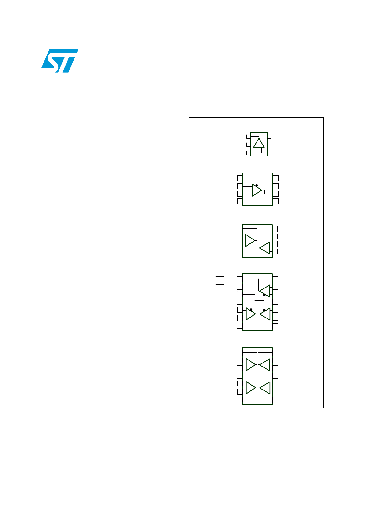
TSH110: SOT23-5
TSH110: SOT23-5
Output
Output
1
1
VCC -
VCC -
2
2
Non Inverting Input Inverting Input
Non Inverting Input Inverting Input
TSH111: SO-8/TSSOP8
TSH111: SO-8/TSSOP8
TSH111: SO-8/TSSOP8
Inverting Input
Inverting Input
Inverting Input
Non Inverting Input
Non Inverting Input
Non Inverting Input
VCC -
VCC -
VCC -
TSH112: SO-8/TSSOP8
TSH112: SO-8/TSSOP8
TSH112: SO-8/TSSOP8
Output1
Output1
Output1
Inverting Input1 Output2
Inverting Input1 Output2
Inverting Input1 Output2
Non Inverting Input1
Non Inverting Input1
Non Inverting Input1
VCC -
VCC -
VCC -
TSH113: SO-14/TSSOP14
TSH113: SO-14/TSSOP14
TSH113: SO-14/TSSOP14
STANDBY1
STANDBY1
STANDBY1
STANDBY2
STANDBY2
STANDBY2
STANDBY3
STANDBY3
STANDBY3
VCC +
VCC +
VCC +
Non Inverting Input1
Non Inverting Input1
Non Inverting Input1
Inverting Input1
Inverting Input1
Inverting Input1
Output1
Output1
Output1
TSH114: SO-14/TSSOP14
TSH114: SO-14/TSSOP14
TSH114: SO-14/TSSOP14
Output1
Output1
Output1
Inverting Input1
Inverting Input1
Inverting Input1
Non Inverting Input1
Non Inverting Input1
Non Inverting Input1
VCC +
VCC +
VCC +
Non Inverting Input2
Non Inverting Input2
Non Inverting Input2
Inverting Input2
Inverting Input2
Inverting Input2
Output2
Output2
Output2
NC
NC
NC
3
3
1
1
1
2
2
2
3
3
3
4
4
4
1
1
1
2
2
2
_
_
_
+
+
+
3
3
3
4
4
4
1
1
1
2
2
2
3
3
3
4
4
4
5
5
5
+
+
+
_
_
_
6
6
6
7
7
7
1
1
1
2
2
2
_
_
_
+
+
+
3
3
3
4
4
4
5
5
5
+
+
+
_
_
_
6
6
6
7
7
7
5
5
VCC +
VCC +
+ -
+ -
4
4
8
8
8
STANDBY
STANDBY
STANDBY
_
_
_
+
+
+
7
7
7
VCC +
VCC +
VCC +
Output
Output
Output
6
6
6
NC
NC
NC
5
5
5
VCC +
VCC +
VCC +
8
8
8
7
7
7
Inverting Input2
Inverting Input2
Inverting Input2
6
6
6
_
_
_
+
+
+
Non Inverting Input2
Non Inverting Input2
Non Inverting Input2
5
5
5
14
14
14
Output3
Output3
Output3
13
13
13
Inverting Input3
Inverting Input3
Inverting Input3
_
_
_
+
+
+
Non Inverting Input3
Non Inverting Input3
Non Inverting Input3
12
12
12
VCC -
VCC -
VCC -
11
11
11
10
10
10
Non Inverting Input2
Non Inverting Input2
Non Inverting Input2
+
+
+
_
_
_
Inverting Input2
Inverting Input2
Inverting Input2
9
9
9
Output2
Output2
Output2
8
8
8
14
14
14
Output4
Output4
Output4
13
13
13
Inverting Input4
Inverting Input4
Inverting Input4
_
_
_
+
+
+
Non Inverting Input4
Non Inverting Input4
Non Inverting Input4
12
12
12
11
11
11
VCC -
VCC -
VCC -
10
10
10
Non Inverting Input3
Non Inverting Input3
Non Inverting Input3
+
+
+
_
_
_
Inverting Input3
Inverting Input3
Inverting Input3
9
9
9
Output3
Output3
Output3
8
8
8
The TSH111 comes in SO-8 and TSSOP8
packages, the TSH112 comes in SO-8 and
TSSOP8 packages, the TSH113 and TSH114
come in SO-14 and TSSOP14 packages.
October 2007 Rev 2 1/15
www.st.com
15
Page 2
Absolute maximum ratings and operating conditions TSH110-TSH111-TSH112-TSH113-TSH114
1 Absolute maximum ratings and operating conditions
Table 1. Absolute maximum ratings (AMR
Symbol Parameter Value Unit
(3)
(1)
(2)
14 V
±1 V
±6 V
80
28
22
°C/W
37
32
V
T
T
R
CC
V
V
oper
stg
T
thjc
Supply voltage
id
Differential input voltage
Input voltage
i
Operating free air temperature range -40 to +85 °C
Storage temperature -65 to +150 °C
Maximum junction temperature 150 °C
j
Thermal resistance junction to case
SOT23-5
SO-8
SO-14
TSSOP8
TSSOP14
Thermal resistance junction to ambiant area
SOT23-5
R
thja
SO-8
SO-14
TSSOP8
TSSOP14
HBM: human body model
ESD
CDM: charged device model
Output short circuit duration
1. All voltage values, except differential voltage, are with respect to network ground terminal.
2. Differential voltages are the non-inverting input terminal with respect to the inverting terminal.
3. The magnitude of input and output voltages must never exceed VCC +0.3V
4. Human body model: A 100pF capacitor is charged to the specified voltage, then discharged through a
1.5kΩ resistor between two pins of the device. This is done for all couples of connected pin combinations
while the other pins are floating.
5. Machine model: A 200pF capacitor is charged to the specified voltage, then discharged directly between
two pins of the device with no external series resistor (internal resistor < 5Ω). This is done for all couples of
connected pin combinations while the other pins are floating.
6. Charged device model: all pins and the package are charged together to the specified voltage and then
discharged directly to the ground through only one pin. This is done for all pins.
7. Short-circuits can cause excessive heating and can result in destructive dissipation.
Table 2. Operating conditions
(4)
(5)
(6)
(7)
250
157
125
130
110
2.0
0.2
1.5
°C/W
kVMM: machine model
Symbol Parameter Value Unit
V
CC
V
icm
Supply voltage 5 to 12 V
Common mode input voltage range V
2/15
-
+1.5 to V
CC
+
-1.5 V
CC
Page 3

TSH110-TSH111-TSH112-TSH113-TSH114 Electrical characteristics
2 Electrical characteristics
Table 3. Dual supply voltage, VCC= ±2.5V, R
(1)
fb
= 680Ω, T
= 25°C (unless otherwise
amb
specified)
Symbol Parameter Test conditions Min. Typ. Max. Unit
DC performance
V
Input offset voltage
io
ΔV
R
CMR
SVR
PSR
Input offset voltage drift vs. temperature T
io
I
Non inverting input bias current
ib+
I
Inverting input bias current
ib-
Transimpedance RL=100Ω 500 750 kΩ
OL
I
Supply current per operator
CC
Common mode rejection ratio
ΔV
/ΔVio)
(
ic
Supply voltage rejection ratio
(
ΔV
/ΔVio)
CC
Power supply rejection ratio
ΔV
/ΔV
(
CC
out
)
Dynamic performance and output characteristics
T
amb
T
< T
min
min
T
amb
T
min
T
amb
T
min
T
amb
T
min
Gain=1, R
< T
< T
< T
< T
amb
amb
amb
amb
< T
< T
< T
max
max
max
max
3.2 4 mA
< T
< T
amb
max
=3.9kΩ 48 dB
load
-1.5 0.3 2.0 mV
1mV
5 μV/°C
-10 1.4 13 μA
2.5 μA
-3 1.9 7 μA
2.5 μA
3.5 mA
56 60 dB
70 80 dB
V
High level output voltage
oh
Low level output voltage
V
ol
| I
| Output sink current T
sink
I
source
Output source current T
BW -3dB bandwidth
SR Slew rate
T
amb
RL = 100Ω
T
< T
amb
< T
min
RL = 100Ω GND
T
amb
RL = 100Ω
< T
T
min
amb
< T
RL = 100Ω
< T
< T
amb
amb
< T
< T
fb
min
min
V
out
=1Vpk, R
max
max
max
max
(1)
=820Ω//2pF
1.4 2 V
1.9 V
-1.8 -1.3 V
-1.7 V
20 mA
18 mA
Load=100Ω
=+2 81 MHz
A
VCL
A
=+2, 2V step
VCL
Load=100Ω
160 230 V/μs
3/15
Page 4

Electrical characteristics TSH110-TSH111-TSH112-TSH113-TSH114
Table 3. Dual supply voltage, VCC= ±2.5V, R
(1)
fb
= 680Ω, T
= 25°C (unless otherwise
amb
specified) (continued)
Symbol Parameter Test conditions Min. Typ. Max. Unit
T
Rise time
r
T
Fall time 9ns
f
Ov Overshoot 16 %
for 200mV step
A
VCL
=+2, R
(1)
fb
Load=100Ω
=820Ω//2pF
St Settling time @ 0.05% 60 ns
ΔG Differential gain
Δφ Differential phase 0.05 °
A
=+2, RL=100Ω
VCL
F=4.5MHz, V
out
=1V
peak
Noise and harmonic performance
en Equivalent input voltage noise
Frequency : 1MHz
in Equivalent input current noise 8.5 pA/√Hz
A
=+2, F=2MHz
THD Total harmonic distortion
R
V
A
VCL
L
out
VCL
=100Ω
=2V
=+2, V
peak
out
=2V
pp
RL=100Ω
F1=1MHz, F2=1.1MHz
IM3 Third order inter modulation product
@900kHz 90
@1.2MHz 90
@3.1MHz 86
@3.2MHz 83
9ns
0.05 %
3nV/√Hz
64.4 dB
dBc
Matching characteristics
Gf Gain flatness
F=(DC) to 6MHz
A
VCL
=+2, V
out
=2V
pp
0.1 dB
Vo1/Vo2 Channel separation F=1MHz to 10MHz 65 dB
1. R
is the feedback resistance between the output and the inverting input of the amplifier.
fb
4/15
Page 5
TSH110-TSH111-TSH112-TSH113-TSH114 Electrical characteristics
Table 4. Dual supply voltage, VCC=±6V, R
(1)
= 680Ω, T
fb
= 25°C (unless otherwise specified)
amb
Symbol Parameter Test conditions Min. Typ. Max. Unit
DC performance
V
io
ΔV
I
ib+
I
ib -
R
OL
I
CC
CMR
SVR
PSR
T
Input offset voltage
Input offset voltage drift vs temperature T
io
Non inverting input bias current
Inverting input bias current
T
T
T
T
T
amb
min
min
amb
min
amb
min
< T
< T
< T
< T
amb
amb
amb
amb
< T
< T
< T
< T
max
max
max
max
Transimpedance RL=100Ω 600 900 kΩ
T
Supply current per operator
T
amb
min
< T
amb
< T
max
Common mode rejection ratio
ΔV
/ΔVio)
(
ic
Supply voltage rejection ratio
ΔV
/ΔVio)
(
CC
Power supply rejection ratio
(
ΔV
/ΔV
out
)
CC
Gain=1, R
=3.9kΩ 49 dB
load
-1.0 0.9 3.0 mV
1.3 mV
5 μV/°C
-12 1 14 μA
1.7 μA
-4 3 10 μA
3.4 μA
45mA
4.1 mA
58 63 dB
72 80 dB
Dynamic performance and output characteristics
T
amb
RL = 100Ω
V
High level output voltage
oh
< T
T
min
amb
< T
max
RL = 100Ω
T
amb
RL = 100Ω
Low level output voltage
V
ol
< T
T
min
amb
< T
max
RL = 100Ω
| Output sink current T
| I
sink
I
source
Output source current T
Bw -3dB bandwidth
SR Slew rate
T
Rise time
r
Fall time 12.2 ns
T
f
Ov Overshoot 17 %
< T
< T
amb
amb
< T
< T
fb
max
max
(1)
=680Ω//2pF
min
min
V
out
=1Vpk, R
Load=100Ω
A
=+2 100 MHz
VCL
=+2, 6V step
A
VCL
Load=100Ω
for 200mV step
A
VCL
=+2, R
(1)
=680Ω//2pF
fb
Load=100Ω
4.5 4.7 V
4.6 V
-4.7 -4.3 V
-4.6 V
47 mA
46 mA
240 450 V/μs
10.4 ns
St Settling time @ 0.05% 40 ns
5/15
Page 6

Electrical characteristics TSH110-TSH111-TSH112-TSH113-TSH114
Table 4. Dual supply voltage, VCC=±6V, R
(1)
= 680Ω, T
fb
= 25°C (unless otherwise specified)
amb
Symbol Parameter Test conditions Min. Typ. Max. Unit
ΔG Differential gain
Δφ Differential phase 0.05 °
A
=+2, RL=100Ω
VCL
F=4.5MHz, V
out
=2V
peak
0.05 %
Noise and harmonic performance
en Equivalent input voltage noise
3nV/√Hz
Frequency : 1MHz
in Equivalent input current noise 8.6 pA/√Hz
A
=+2, F=2MHz
THD Total harmonic distortion
VCL
RL=100Ω
V
=4V
out
pp
A
=+2, V
VCL
out
=4V
67.7 dB
pp
RL=100Ω
F1=1MHz, F2=1.1MHz
IM3 Third order inter modulation product
@900kHz 82
dBc
@1.2MHz 84
@3.1MHz 77
@3.2MHz 73
Matching characteristics
Gf Gain flatness
F=(DC) to 6MHz
A
VCL
=+2, V
out
=4V
pp
0.1 dB
Vo1/Vo2 Channel separation F=1MHz to 10MHz 65 dB
1. R
is the feedback resistance between the output and the inverting input of the amplifier.
fb
6/15
Page 7

TSH110-TSH111-TSH112-TSH113-TSH114 Standby mode
3 Standby mode
Table 5. T
= 25°C (unless otherwise specified), VCC=±6V
amb
Symbol Parameter Test cond itio ns Min. Typ. Max. Unit
V
V
I
CC-STBY
Z
T
T
Table 6. TSH111 standby control pin status
Standby low level V
low
Standby high level (V
high
Current consumption per
operator in Standby mode
I
Input/output isolation F=1MHz -90 dB
sol
R
Output impedance (R
out
Time from Standby mode to
on
active mode
Time from active mode to
off
Standby mode
out
// C
out
)
out
C
out
Down to I
CC-STBY
-
CC
-
+2) (V
CC
26 40 μA
31
25
2 μs
=40μA13 μs
(V
CC
-
+0.8) V
+
)V
CC
TSH111 standby control pin 8 (SBY) Operator status
V
low
V
high
Table 7. TSH113 standby control pin status
Standby
Active
MΩ
pF
TSH113 standby control Operator status
pin 1
(SBY
OP1)
V
low
V
high
xV
xV
xxV
xxV
pin 2
(SBY OP2)
pin 3
(SBY OP)
x x Standby x x
xxActivexx
low
high
x x Standby x
low
high
OP1 OP1 OP3
xActivex
x x Standby
xxActive
7/15
Page 8

Package information TSH110-TSH111-TSH112-TSH113-TSH114
4 Package information
In order to meet environmental requirements, STMicroelectronics offers these devices in
ECOPACK
category of second level interconnect is marke d on the pa ckage and on the inner box label,
in compliance with JEDEC Standard JESD97. The maximum ratings related t o soldering
conditions are also marked on the inner box label. ECOPACK is an STMicroelectronics
trademark. ECOPACK specifications are available at: www.st.com
®
packages. These packages have a lead-free second level interconnect. The
.
8/15
Page 9

TSH110-TSH111-TSH112-TSH113-TSH114 Package information
4.1 SO-8 package mechanical data
Figure 1. SO-8 package mechanical data
Dimensions
Ref.
Min. Typ. Max. Min. Typ. Max.
A1.750.069
A1 0.10 0.25 0.004 0.010
A2 1.25 0.049
b 0.28 0.48 0.011 0.019
c 0.17 0.23 0.007 0.010
D 4.80 4.90 5.00 0.189 0.193 0.197
H 5.80 6.00 6.20 0.228 0.236 0.244
E1 3.80 3.90 4.00 0.150 0.154 0.157
e 1.27 0.050
h 0.25 0.50 0.010 0.020
L 0.40 1.27 0.016 0.050
k1°8°1°8°
ccc 0.10 0.004
Millimeters Inches
9/15
Page 10

Package information TSH110-TSH111-TSH112-TSH113-TSH114
4.2 TSSOP8 package mechanical data
Figure 2. TSSOP8 package mechanical data
Dimensions
Ref.
Min. Typ. Max. Min. Typ. Max.
A 1.2 0.047
A1 0.05 0.15 0.002 0.006
A2 0.80 1.00 1.05 0.031 0.039 0.041
b 0.19 0.30 0.007 0.012
c 0.09 0.20 0.004 0.008
D 2.90 3.00 3.10 0.114 0.118 0.122
E 6.20 6.40 6.60 0.244 0.252 0.260
E1 4.30 4.40 4.50 0.169 0.173 0.177
e 0.65 0.0256
k0°8°0°8°
L 0.45 0.60 0.75 0.018 0.024 0.030
L1 1 0.039
aaa 0.1 0.004
Millimeters Inches
10/15
Page 11

TSH110-TSH111-TSH112-TSH113-TSH114 Package information
4.3 SO-14 package mechanical data
Figure 3. SO-14 package mechanical data
Dimensions
Ref.
Min. Typ. Max. Min. Typ. Max.
A1.750.068
a1 0.1 0.2 0.003 0.007
a2 1.65 0.064
b 0.35 0.46 0.013 0.018
b1 0.19 0.25 0.007 0.010
C0.5 0.019
c1 45° (typ.)
D 8.55 8.75 0.336 0.344
E 5.8 6.2 0.228 0.244
e 1.27 0.050
e3 7.62 0.300
F 3.8 4.0 0.149 0.157
G 4.6 5.3 0.181 0.208
L 0.5 1.27 0.019 0.050
M0.680.026
Millimeters Inches
S 8° (max.)
11/15
Page 12

Package information TSH110-TSH111-TSH112-TSH113-TSH114
4.4 TSSOP14 package mechanical data
Figure 4. TSSOP14 package mechanical data
Dimensions
Ref.
Millimeters Inches
Min. Typ. Max. Min. Typ. Max.
A 1.2 0.047
A1 0.05 0.15 0.002 0.004 0.006
A2 0.8 1 1.05 0.031 0.039 0.041
b 0.19 0.30 0.007 0.012
c 0.09 0.20 0.004 0.0089
D 4.9 5 5.1 0.193 0.197 0.201
E 6.2 6.4 6.6 0.244 0.252 0.260
E1 4.3 4.4 4.48 0.169 0.173 0.176
e 0.65 BSC 0.0256 BSC
K0°8°0°8°
L 0.45 0.60 0.75 0.018 0.024 0.030
A2
A
A1
b
e
c
K
L
E
D
PIN 1 IDENTIFICATION
1
12/15
E1
Page 13

TSH110-TSH111-TSH112-TSH113-TSH114 Package information
4.5 SOT23-5 package mechanical data
Figure 5. SOT23-5 package (Inches)
Dimensions
Ref.
Min. Typ. Max. Min. Typ. Max.
A 0.90 1.45 0.035 0.057
A1 0.00 0.15 0.00 0.006
A2 0.90 1.30 0.035 0.051
b 0.35 0.50 0.014 0.02
C 0.09 0.20 0.003 0.008
D 2.80 3.00 0.110 0.118
H 2.60 3.00 0.102 0.118
E 1.50 1.75 0.059 0.069
e 0.95 0.037
e1 1.9 0.075
L 0.35 0.55 0.014 0.022
Millimeters Inches
.
13/15
Page 14

Ordering information TSH110-TSH111-TSH112-TSH113-TSH114
5 Ordering information
Table 8. Order codes
Part number Temperature range Package Packing Marking
TSH110ILT
TSH110IYLT
TSH111ID
TSH111IDT
TSH111IPT
TSH112ID
TSH112IDT
TSH112IPT
TSH113ID
TSH113IDT
(1)
(Thin shrink outline package)
-40°C to +85°C
(Thin shrink outline package)
SOT23-5 Tape & reel K302
SOT23-5
(Automotive grade level)
SO-8
TSSOP8
SO-8
TSSOP8
SO-14
Tape & reel K309
Tube or
Tape & reel
Tape & reel H111I
Tube or
Tape & reel
Tape & reel H112I
Tube or
Tape & reel
H111I
H112I
TSH113I
TSH113IPT TSSOP14 Tape & reel TSH113I
TSH114ID
TSH114IDT
SO-14
Tube or
Tape & reel
TSH114I
TSH114IPT TSSOP14 Tape & reel TSH114I
1. Qualification and characterization according to AEC Q100 and Q003 or equivalent, advanced screening according to AEC
Q001 & Q 002 or equivalent are on-going.
6 Revision history
Table 9. Document revision history
4-Oct-2001 1 Initial release.
22-Oct-2007 2
14/15
Date Revision Changes
Added TSH110ILT/TSH110IYLT order codes to Table 8: Order codes.
Document reformatted.
Page 15

TSH110-TSH111-TSH112-TSH113-TSH114
Please Read Carefully:
Information in this document is provided solely in connection with ST products. STMicroelectronics NV and its subsidiaries (“ST”) reserve the
right to make changes, corrections, modifications or improvements, to this document, and the products and services described herein at any
time, without notice.
All ST products are sold pursuant to ST’s terms and conditions of sale.
Purchasers are solely res ponsibl e fo r the c hoic e, se lecti on an d use o f the S T prod ucts and s ervi ces d escr ibed he rein , and ST as sumes no
liability whatsoever relati ng to the choice, selection or use o f the ST products and services desc ribed herein.
No license, express or implied, by estoppel or otherwise, to any intellectual property rights is granted under this document. If any part of this
document refers to any third pa rty p ro duc ts or se rv ices it sh all n ot be deem ed a lice ns e gr ant by ST fo r t he use of su ch thi r d party products
or services, or any intellectua l property c ontained the rein or consi dered as a warr anty coverin g the use in any manner whats oever of suc h
third party products or servi ces or any intellectual property contained therein.
UNLESS OTHERWISE SET FORTH IN ST’S TERMS AND CONDITIONS OF SALE ST DISCLAIMS ANY EXPRESS OR IMPLIED
WARRANTY WITH RESPECT TO THE USE AND/OR SALE OF ST PRODUCTS INCLUDING WITHOUT LIMITATION IMPLIED
WARRANTIES OF MERCHANTABILITY, FITNESS FOR A PARTICUL AR PURPOS E (AND THEIR EQUIVALE NTS UNDER THE LAWS
OF ANY JURISDICTION), OR INFRINGEMENT OF ANY PATENT, COPYRIGHT OR OTHER INTELLECTUAL PROPERTY RIGHT.
UNLESS EXPRESSLY APPROVED IN WRITING BY AN AUTHORIZED ST REPRESENTATIVE, ST PRODUCTS ARE NOT
RECOMMENDED, AUTHORIZED OR WARRANTED FOR USE IN MILITARY, AIR CRAFT, SPACE, LIFE SAVING, OR LIFE SUSTAINING
APPLICATIONS, NOR IN PRODUCTS OR SYSTEMS WHERE FAILURE OR MALFUNCTION MAY RESULT IN PERSONAL INJ URY,
DEATH, OR SEVERE PROPERTY OR ENVIRONMENTAL DAMAGE. ST PRODUCTS WHICH ARE NOT SPECIFIED AS "AUTOMOTIVE
GRADE" MAY ONLY BE USED IN AUTOMOTIVE APPLICATIONS AT USER’S OWN RISK.
Resale of ST products with provisions different from the statements and/or technical features set forth in this document shall immediately void
any warranty granted by ST fo r the ST pro duct or serv ice describe d herein and shall not cr eate or exten d in any manne r whatsoever , any
liability of ST.
ST and the ST logo are trademarks or registered trademarks of ST in various countries.
Information in this document su persedes and replaces all information previously supplied.
The ST logo is a registered trademark of STMicroelectronics. All other names are the property of their respective owners.
© 2007 STMicroelectronics - All rights reserved
STMicroelectronics group of compan ie s
Australia - Belgium - Brazil - Canada - China - Czech Republic - Finland - France - Germany - Hong Kong - India - Israel - Italy - Japan -
Malaysia - Malta - Morocco - Singapore - Spain - Sweden - Switzerland - United Kingdom - United States of America
www.st.com
15/15
 Loading...