

Features
TS982
Wide bandwidth dual bipolar operational amplifier
■ Operating from V
■ 200 mA output current on each amplifier
■ High dissipation package
■ Rail-to-rail input and output
■ Unity-gain stable
= 2.5 V to 5.5 V
CC
Applications
■ Hall sensor compensation coil
■ Servo amplifier
■ Motor driver
■ Industrial
■ Automotive
Description
The TS982 is a dual operational amplifier able to
drive 200 mA down to voltages as low as 2.7 V.
The SO-8 exposed-pad package allows high
current output at high ambient temperatures
making it a reliable solution for automotive and
industrial applications.
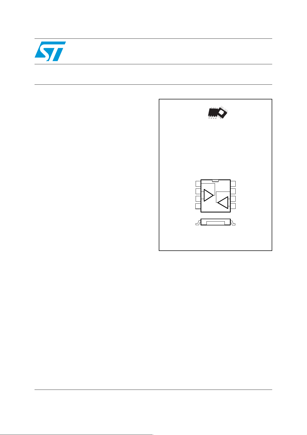
DW
SO-8 exposed-pad
(Plastic micropackage)
Pin connections (top view)
Output1
Output1
1
1
2
Inverting Input1 Output2
Inverting Input1 Output2
Non Inverting Input1
Non Inverting Input1
This pad can be connected to a (-Vcc) copper area on the PCB
This pad can be connected to a (-Vcc) copper area on the PCB
2
-
-
+
+
3
3
VCC -
VCC -
4
4
Cross Section View Showing Exposed-Pad
Cross Section View Showing Exposed-Pad
VCC +
VCC +
8
8
7
7
Inverting Input2
Inverting Input2
6
6
-
-
+
+
Non Inverting Input2
Non Inverting Input2
5
5
The TS982 is stable with a unity gain.
June 2008 Rev 6 1/20
www.st.com
20

Contents TS982
Contents
1 Absolute maximum ratings and operating conditions . . . . . . . . . . . . . 3
2 Electrical characteristics . . . . . . . . . . . . . . . . . . . . . . . . . . . . . . . . . . . . . 4
3 Application information . . . . . . . . . . . . . . . . . . . . . . . . . . . . . . . . . . . . . 14
3.1 Exposed-pad package description . . . . . . . . . . . . . . . . . . . . . . . . . . . . . . 14
3.2 Exposed-pad electrical connection . . . . . . . . . . . . . . . . . . . . . . . . . . . . . 14
3.3 Thermal management benefits . . . . . . . . . . . . . . . . . . . . . . . . . . . . . . . . 15
3.4 Thermal management guidelines . . . . . . . . . . . . . . . . . . . . . . . . . . . . . . . 15
3.5 Parallel operation . . . . . . . . . . . . . . . . . . . . . . . . . . . . . . . . . . . . . . . . . . . 16
4 Package information . . . . . . . . . . . . . . . . . . . . . . . . . . . . . . . . . . . . . . . . 17
5 Ordering information . . . . . . . . . . . . . . . . . . . . . . . . . . . . . . . . . . . . . . . 19
6 Revision history . . . . . . . . . . . . . . . . . . . . . . . . . . . . . . . . . . . . . . . . . . . 19
2/20
TS982 Absolute maximum ratings and operating conditions
1 Absolute maximum ratings and operating conditions
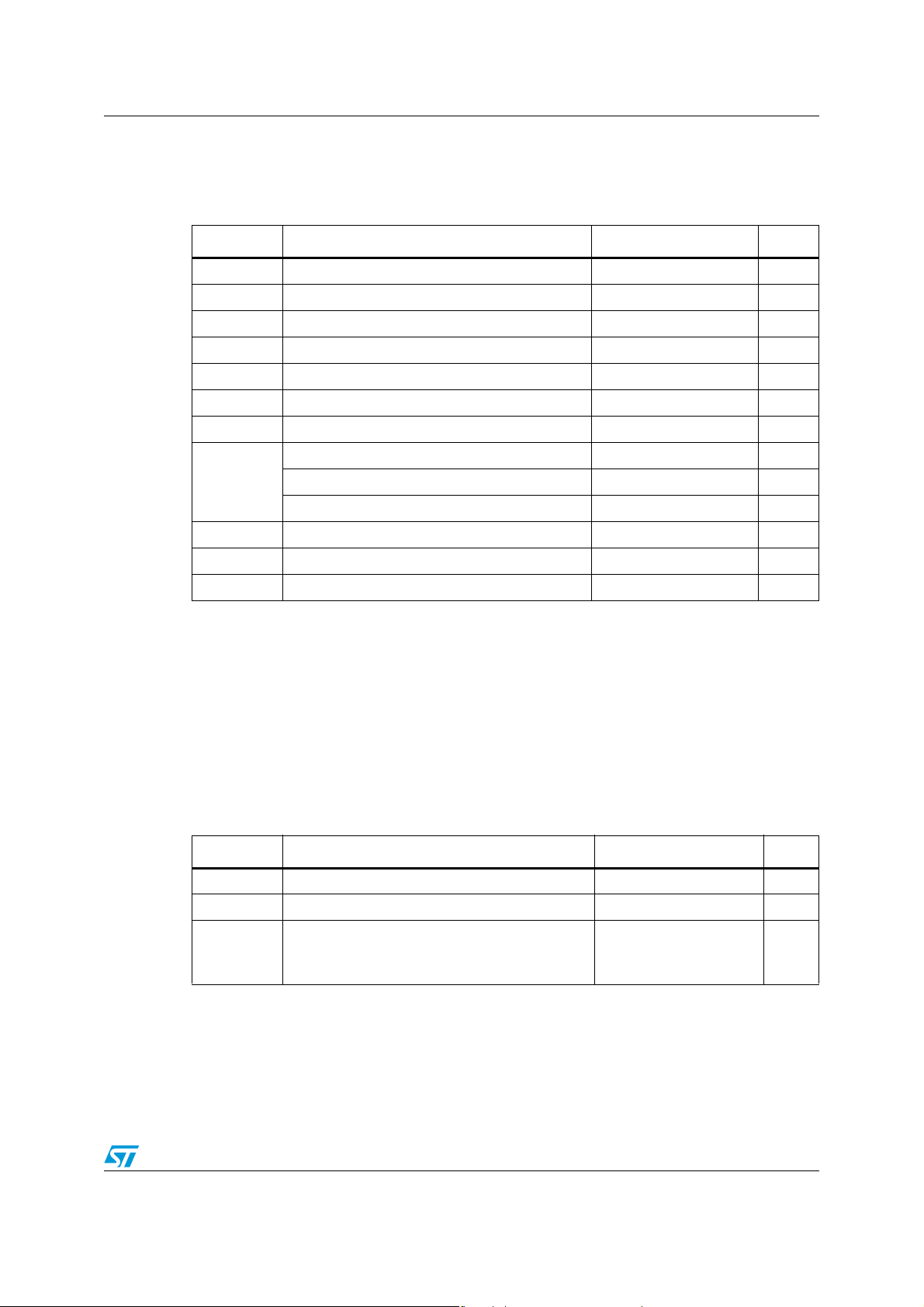
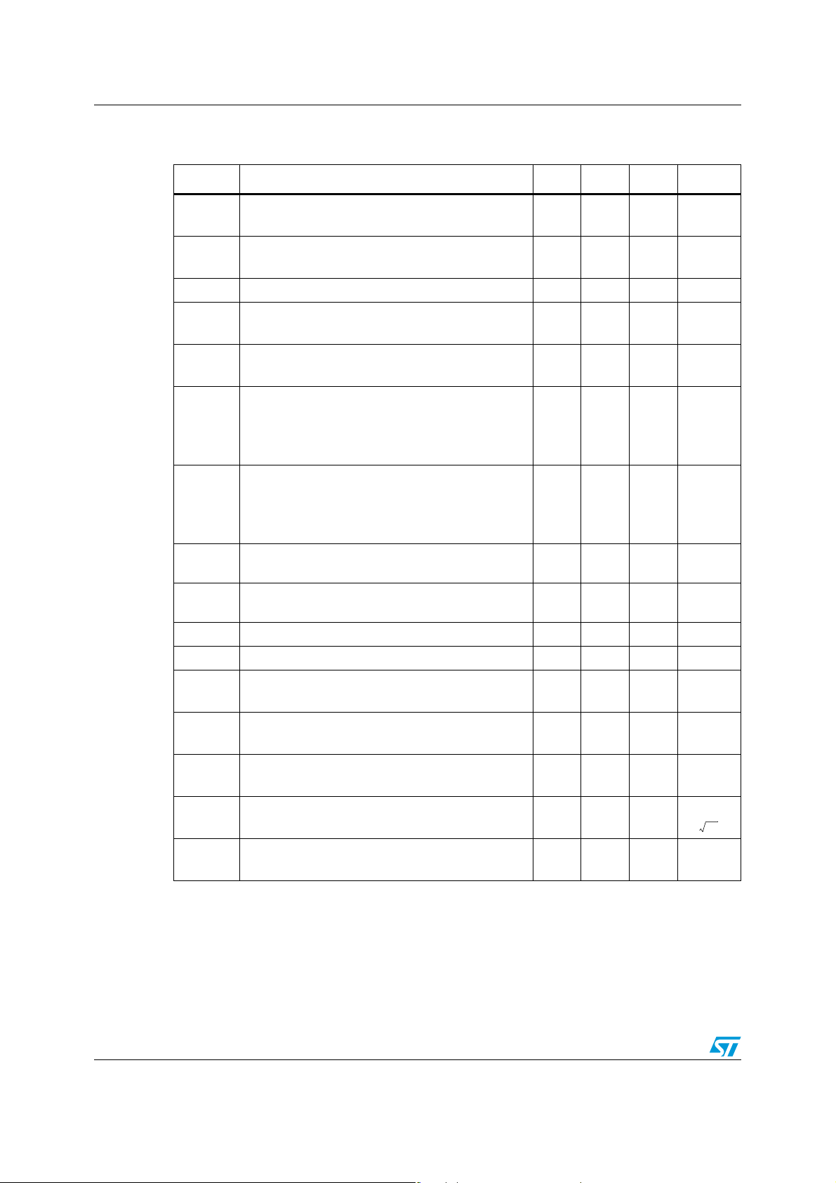
Table 1. Absolute maximum ratings (AMR)
Symbol Parameter Value Unit
V
T
T
R
R
CC
V
oper
stg
T
thja
thjc
in
j
Supply voltage
Input voltage -0.3 V to V
Operating free-air temperature range -40 to + 125 °C
Storage temperature -65 to +150 °C
Maximum junction temperature 150 °C
Thermal resistance junction to ambient
Thermal resistance junction to case 10 °C/W
Human body model (HBM)l
ESD
Charged device model (CDM)
Machine model (MM)
Latch-up Latch-up immunity (all pins) 200 mA
Lead temperature (soldering, 10sec) 250 °C
Output short-circuit duration see note
1. All voltage values are measured with respect to the ground pin.
2. With two sides, two-plane PCB following the EIA/JEDEC JESD51-7 standard.
3. Human body model: A 100 pF capacitor is charged to the specified voltage, then discharged through a
1.5 kΩ resistor between two pins of the device. This is done for all couples of connected pin combinations
while the other pins are floating.
4. Charged device model: all pins and the package are charged together to the specified voltage and then
discharged directly to the ground through only one pin. This is done for all pins.
5. Machine model: A 200pF capacitor is charged to the specified voltage, then discharged directly between
two pins of the device with no external series resistor (internal resistor < 5 Ω). This is done for all couples of
connected pin combinations while the other pins are floating.
6. Short-circuits can cause excessive heating. Destructive dissipation can result from a short-circuit on one or
two amplifiers simultaneously.
Table 2. Operating conditions
(1)
(5)
(3)
(4)
(2)
6V
+0.3 V V
CC
45 °C/W
2kV
1.5 kV
200 V
(6)
Symbol Parameter Value Unit
V
CC
V
icm
Supply voltage 2.5 to 5.5 V
Common mode input voltage range GND to V
CC
V
Load capacitor
C
L
R
< 100 Ω
L
> 100 Ω
R
L
400
100
pF
3/20
Electrical characteristics TS982
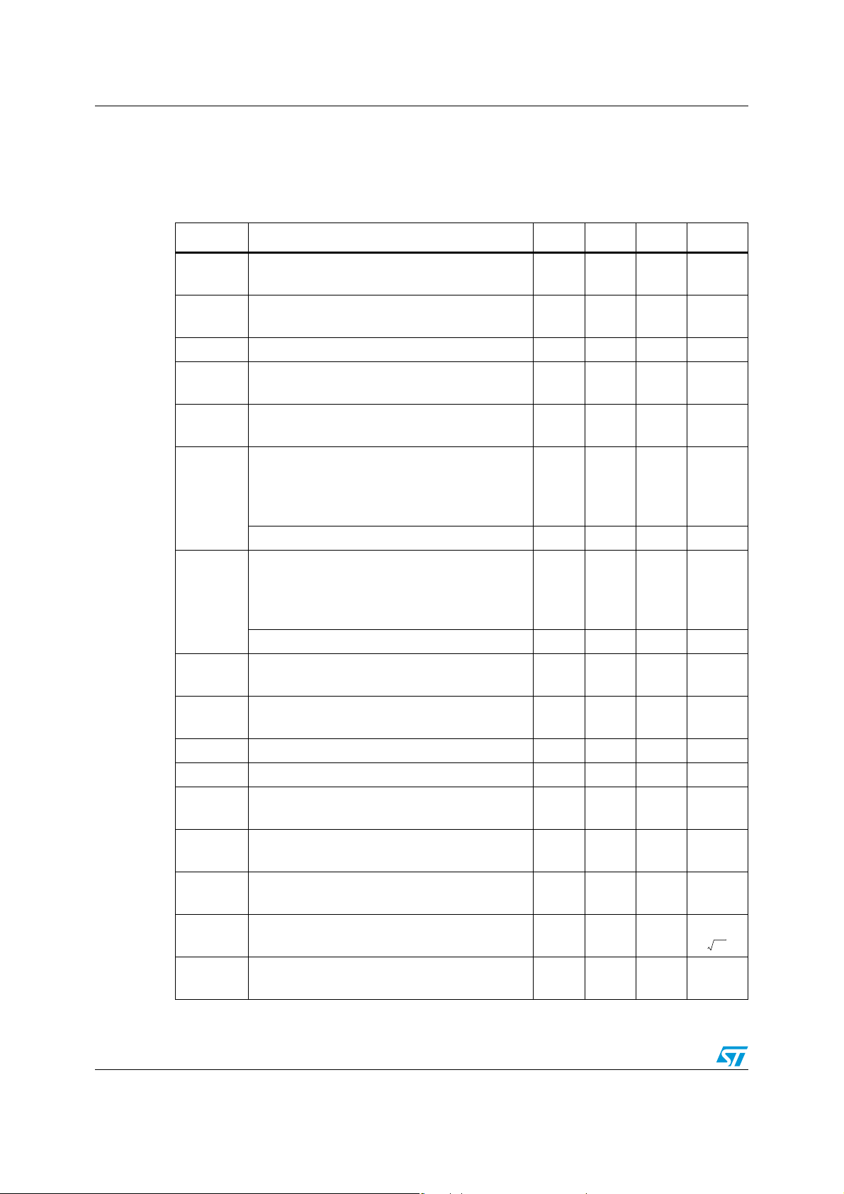
2 Electrical characteristics
Table 3. Electrical characteristics for V
(unless otherwise specified)
Symbol Parameter Min. Typ. Max. Unit
= +5 V, V
CC+
= 0 V, and T
CC-
amb
= 25° C
V
ΔV
I
CC
I
I
Supply current - No input signal, no load
< Top < T
T
min
Input offset voltage (V
IO
IO
< Top < T
T
min
Input offset voltage drift 2 µV/°C
Input bias current - V
IB
T
min
< Top < T
max
max
max
icm
= VCC/2
icm
= VCC/2)
Input offset current
IO
V
icm
= VCC/2
5.5 7.2
7.2
15
7
200 500
500
10 nA
mA
mV
nA
High level output voltage
RL = 16Ω
R
V
OH
= 16Ω, T
L
I
= 200mA
out
VCC= 4.75V, T = 125° C, I
< Top < T
min
max
= 25mA 4.3 V
out
4.2
4
4.4
4
V
Low level output voltage
0.5510.65
0.95
95 dB
V
V
OL
A
VD
GBP
RL = 16Ω
R
= 16Ω, T
L
I
= 200mA
out
V
= 4.75V, T = 125°C, I
CC
< Top < T
min
Large signal voltage gain
= 16Ω
R
L
Gain bandwidth product
R
= 32Ω
L
max
= 25mA 0.45 V
out
1.35 2.2 MHz
CMR Common mode rejection ratio 80 dB
SVR Supply voltage rejection ratio 95 dB
SR
Φ
G
e
Crosstalk
Slew rate, unity gain inverting
= 16Ω
R
L
Phase margin at unit gain
m
= 16Ω, CL = 400pF
R
L
Gain margin
m
= 16Ω, CL = 400pF
R
L
Equivalent input noise voltage
n
F = 1kHz
Channel separation
= 16Ω, F = 1kHz
R
L
4/20
0.45 0.7 V/µs
56 degrees
18 dB
nV
17
----------- Hz
100 dB
TS982 Electrical characteristics
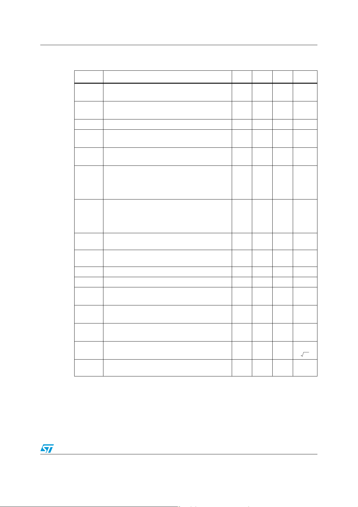
Table 4. Electrical characteristics for V
(unless otherwise specified)
Symbol
Table 5. Parameter
(1)
CC+
= +3.3 V, V
= 0 V, and T
CC-
amb
= 25° C
Min. Typ. Max. Unit
ΔV
I
V
CC
I
I
Supply current - No input signal, no load
T
< Top < T
min
Input offset voltage (V
IO
T
< Top < T
min
Input offset voltage drift 2 µV/°C
IO
Input bias current - V
IB
T
min
< Top < T
max
max
max
= VCC/2)
icm
= VCC/2
icm
Input offset current
IO
V
icm
= VCC/2
5.3 7.2
7.2
15
7
200 500
500
10 nA
mA
mV
nA
High level output voltage
= 16Ω
R
V
OH
L
R
= 16Ω, T
L
I
= 200 mA
out
< Top < T
min
max
2.68
2.64
2.85
2.3
V
Low level output voltage
V
OL
A
VD
GBP
= 16Ω
R
L
R
= 16Ω, T
L
I
= 200mA
out
< Top < T
min
Large signal voltage gain
RL = 16Ω
Gain bandwidth product
R
= 32Ω
L
0.45
max
92 dB
1.2 2 MHz
0.52
0.65
V
1
CMR Common mode rejection ratio 75 dB
SVR Supply voltage rejection ratio 95 dB
SR
Φ
G
e
Crosstalk
1. All electrical values are guaranteed by correlation with measurements at 2.7 V and 5 V.
Slew rate, unity gain inverting
= 16Ω
R
L
Phase margin at unit gain
m
= 16Ω, CL = 400pF
R
L
Gain margin
m
= 16Ω, CL = 400pF
R
L
Equivalent input noise voltage
n
F = 1kHz
Channel separation
= 16Ω, F = 1kHz
R
L
0.45 0.7 V/µs
57 degrees
16 dB
17
100 dB
5/20
nV
----------- Hz
Electrical characteristics TS982
Table 6. Electrical characteristics for VCC = +2.7 V, V
= 0 V, and T
CC-
amb
= 25° C
(unless otherwise specified)
Symbol Parameter Min. Typ. Max. Unit
I
V
ΔV
CC
I
IB
I
IO
Supply current - No input signal, no load
T
< Top < T
min
Input offset voltage (V
IO
T
< Top < T
min
Input offset voltage drift 2 µV/°C
IO
Input bias current - V
< Top < T
T
min
ma
max
max
= VCC/2)
icm
= VCC/2
icm
Input offset current
= VCC/2
V
icm
5.3 6.4
6.4
15
7
200 500
500
10 nA
mA
mV
nA
High level output voltage
= 16Ω
R
V
OH
L
R
= 16Ω, T
L
I
= 20 mA
out
< Top < T
min
max
2.3
2.25
2.85
2.3
V
Low level output voltage
V
OL
A
VD
GBP
= 16Ω
R
L
R
= 16Ω, T
L
I
= 200mA
out
< Top < T
min
Large signal voltage gain
RL = 16Ω
Gain bandwidth product
R
= 32Ω
L
max
1.2 2 MHz
0.4510.37
0.42
92 dB
V
CMR Com mo n mo de r ejection ratio 75 dB
SVR Supply voltage rejection ratio 95 dB
SR
Φ
G
e
Crosstalk
Slew rate, unity gain inverting
= 16Ω
R
L
Phase margin at unit gain
m
= 16Ω, CL = 400pF
R
L
Gain margin
m
= 16 Ω, CL = 400pF
R
L
Equivalent input noise voltage
n
F = 1kHz
Channel separation
RL = 16Ω, F = 1kHz
6/20
0.45 0.7 V/µs
57 degrees
16 dB
nV
17
----------- Hz
100 dB

TS982 Electrical characteristics
Vicm = Vcc/2
Vid = 100mV
Isource = 200mA
Testboard
Figure 1. Current consumption vs. supply
voltage
No load
Ta=125 C
Ta=25 C
Ta=-40 C
Figure 3. Voltage drop vs. output sinking
current
Vcc = 2.7V to 5V
Vicm = Vcc/2
Vid = 100mV
Output Sinking
Testboard PCB
Figure 2. Voltage drop vs. output sourcing
current
Vcc = 2.7V to 5V
Vicm = Vcc/2
Vid = 100mV
Output Sourcing
Testboard PCB
Figure 4. V oltage drop vs. supply voltage
(sourcing)
Figure 5. Voltage drop vs. supply voltage
(sinking)
Vicm = Vcc/2
Vid = 100mV
Isink = 200mA
Testboard
Figure 6. V oltage drop vs. temperature
(I
=50mA)
out
Vcc = 5V
Vicm = Vcc/2
Vid = 100mV
Iout= 50mA
7/20

Electrical characteristics TS982
0.1 1 10 100 1000 10000
-40
-20
0
20
40
60
80
-20
0
20
40
60
80
100
120
140
160
180
Gain (dB)
Frequency (kHz)
Vcc = 5V
RL = 8Ω
Tamb = 25°C
Gain
Phase
Phase (Deg)
0.1 1 10 100 1000 10000
-40
-20
0
20
40
60
80
-20
0
20
40
60
80
100
120
140
160
180
Gain (dB)
Frequency (kHz)
Vcc = 5V
RL = 16Ω
Tamb = 25°C
Gain
Phase
Phase (Deg)
Figure 7. Voltage drop vs. temperature
(I
=100mA)
out
Vcc = 5V
Vicm = Vcc/2
Vid = 100mV
Iout= 100mA
Figure 9. Open loop gain and phase vs.
frequency
80
60
40
Phase
20
Gain (dB)
0
-20
-40
0.1 1 10 100 1000 10000
Gain
Frequency (kHz)
Vcc = 2.7V
RL = 8Ω
Tamb = 25°C
180
160
140
120
100
80
60
40
20
0
-20
Figure 8. V oltage drop vs. temperature
(I
= 200 mA)
out
Figure 10. Open loop gain and phase vs.
frequency
Phase (Deg)
Vcc = 5V
Vicm = Vcc/2
Vid = 100mV
Iout= 200mA
Figure 11. Open loop gain and phase vs.
frequency
80
60
40
Phase
20
Gain (dB)
0
-20
-40
0.1 1 10 100 1000 10000
8/20
Gain
Frequency (kHz)
Vcc = 2.7V
RL = 16Ω
Tamb = 25°C
180
160
140
120
100
80
60
40
20
0
-20
Figure 12. Open loop gain and phase vs.
frequency
Phase (Deg)

TS982 Electrical characteristics
0.1 1 10 100 1000 10000
-40
-20
0
20
40
60
80
-20
0
20
40
60
80
100
120
140
160
180
Gain (dB)
Frequency (kHz)
Vcc = 5V
RL = 32Ω
Tamb = 25°C
Gain
Phase
Phase (Deg)
0.1 1 10 100 1000 10000
-40
-20
0
20
40
60
80
-20
0
20
40
60
80
100
120
140
160
180
Gain (dB)
Frequency (kHz)
Vcc = 5V
RL = 600
Ω
Tamb = 25°C
Gain
Phase
Phase (Deg)
0.1 1 10 100 1000 10000
-40
-20
0
20
40
60
80
-20
0
20
40
60
80
100
120
140
160
180
Gain (dB)
Frequency (kHz)
Vcc = 5V
RL = 5k
Ω
Tamb = 25°C
Gain
Phase
Phase (Deg)
Figure 13. Open loop gain and phase vs.
frequency
80
60
40
20
Gain (dB)
0
-20
-40
0.1 1 10 100 1000 10000
Phase
Gain
Frequency (kHz)
Vcc = 2.7V
RL = 32Ω
Tamb = 25°C
180
160
140
120
100
80
60
40
20
0
-20
Figure 15. Open loop gain and phase vs.
frequency
80
60
40
20
Gain (dB)
0
-20
-40
0.1 1 10 100 1000 10000
Phase
Gain
Frequency (kHz)
Vcc = 2.7V
RL = 600Ω
Tamb = 25°C
180
160
140
120
100
80
60
40
20
0
-20
Figure 14. Open loop gain and phase vs.
frequency
Phase (Deg)
Figure 16. Open loop gain and phase vs.
frequency
Phase (Deg)
Figure 17. Open loop gain and phase vs.
frequency
80
60
40
20
Gain (dB)
0
-20
-40
0.1 1 10 100 1000 10000
Phase
Gain
Frequency (kHz)
Vcc = 2.7V
RL = 5k
Tamb = 25°C
Figure 18. Open loop gain and phase vs.
frequency
180
160
Ω
140
120
100
80
60
Phase (Deg)
40
20
0
-20
9/20

Electrical characteristics TS982
2.0 2.5 3.0 3.5 4.0 4.5 5.0
0
10
20
30
40
50
CL=0 to 500pF
RL=8
Ω
Tamb=25°C
Gain Margin (dB)
Power Supply Voltage (V)
2.0 2.5 3.0 3.5 4.0 4.5 5.0
0
10
20
30
40
50
CL=0 to 500pF
RL=16
Ω
Tamb=25°C
Gain Margin (dB)
Power Supply Voltage (V)
2.0 2.5 3.0 3.5 4.0 4.5 5.0
0
10
20
30
40
50
CL=0 to 500pF
RL=32
Ω
Tamb=25°C
Gain Margin (dB)
Power Supply Voltage (V)
Figure 19. Phase margin vs. supply voltage Figure 20. Gain margin vs. supply voltage
50
RL=8
Ω
Tamb=25°C
40
30
20
Phase Margin (Deg)
10
0
2.0 2.5 3.0 3.5 4.0 4.5 5.0
CL= 0 to 500pF
Power Supply Voltage (V)
Figure 21. Phase margin vs. supply voltage Figure 22. Gain margin vs. supply voltage
50
40
30
CL= 0 to 500pF
20
Phase Margin (Deg)
10
RL=16
Ω
Tamb=25°C
0
2.0 2.5 3.0 3.5 4.0 4.5 5.0
Power Supply Voltage (V)
Figure 23. Phase margin vs. supply voltage Figure 24. Gain margin vs. supply voltage
50
40
30
20
Phase Margin (Deg)
10
RL=32
Ω
Tamb=25°C
0
2.0 2.5 3.0 3.5 4.0 4.5 5.0
CL= 0 to 500pF
Power Supply Voltage (V)
10/20

TS982 Electrical characteristics
2.0 2.5 3.0 3.5 4.0 4.5 5.0
0
10
20
CL=500pF
CL=200pF
CL=100pF
CL=0pF
RL=600
Ω
Tamb=25°C
Gain Margin (dB)
Power Supply Voltage (V)
2.0 2.5 3.0 3.5 4.0 4.5 5.0
0
10
20
CL=500pF
CL=200pF
CL=100pF
CL=0pF
RL=5k
Ω
Tamb=25°C
Gain Margin (dB)
Power Supply Voltage (V)
Figure 25. Phase margin vs. supply voltage Figure 26. Gain margin vs. supply voltage
70
60
50
40
CL=0pF
CL=500pF
30
20
Phase Margin (Deg)
10
RL=600
Ω
Tamb=25°C
0
2.0 2.5 3.0 3.5 4.0 4.5 5.0
Power Supply Voltage (V)
Figure 27. Phase margin vs. supply voltage Figure 28. Gain margin vs. supply voltage
70
60
50
CL=0pF
40
CL=300pF CL=500pF
30
20
Phase Margin (Deg)
10
RL=5k
Ω
Tamb=25°C
0
2.0 2.5 3.0 3.5 4.0 4.5 5.0
Power Supply Voltage (V)
Figure 29. Distortion vs. output voltage Figure 30. Distortion vs. output voltage
RL = 4
RL = 2
Ω
F = 1kHz
Av = +1
BW < 80kHz
Tamb = 25°C
Vcc=2.7V
Vcc=3.3V
Vcc=5V
Ω
F = 1kHz
Av = +1
BW < 80kHz
Tamb = 25°C
Vcc=2.7V
Vcc=3.3V
Vcc=5V
11/20

Electrical characteristics TS982
100 1000 10000
0
20
40
60
80
100
120
ChB to ChA & ChA to Chb
RL=600
Ω
Vcc=5V
Vout=1.4Vrms
Av=-1
Bw < 125kHz
Tamb=25°C
20k20
Crosstalk (dB)
Frequency (Hz)
Figure 31. Distortion vs. output voltage Figure 32. Distortion vs. output voltage
RL = 8
Ω
F = 1kHz
Av = +1
BW < 80kHz
Tamb = 25°C
Vcc=2.7V
Vcc=3.3V
Vcc=5V
RL = 16
Ω
F = 1kHz
Av = +1
BW < 80kHz
Tamb = 25°C
Vcc=2.7V
Vcc=3.3V
Vcc=5V
Figure 33. Crosstalk vs. frequency Figure 34. Crosstalk vs. frequency
Crosstalk (dB)
100
80
ChB to ChA
ChA to ChB
60
RL=8
40
Ω
Vcc=5V
Pout=100mW
20
Av=-1
Bw < 125kHz
Tamb=25°C
100 1000 10000
20k20
Frequency (Hz)
Crosstalk (dB)
100
80
60
40
20
100 1000 10000
Frequency (Hz)
ChB to ChA
ChA to ChB
RL=16
Ω
Vcc=5V
Pout=90mW
Av=-1
Bw < 125kHz
Tamb=25°C
20k20
Figure 35. Crosstalk vs. frequency Figure 36. Crosstalk vs. frequency
100
80
60
40
Crosstalk (dB)
20
12/20
ChB to ChA & ChA to Chb
RL=32
Ω
Vcc=5V
Pout=60mW
Av=-1
Bw < 125kHz
Tamb=25°C
100 1000 10000
Frequency (Hz)
20k20

TS982 Electrical characteristics
Figure 37. Crosstalk vs. frequency Figure 38. Equivalent input noise voltage vs.
frequency
120
100
80
60
40
Crosstalk (dB)
20
0
ChB to ChA & ChA to Chb
RL=5kΩ
Vcc=5V
Vout=1.5Vrms
Av=-1
Bw < 125kHz
Tamb=25°C
100 1000 10000
Frequency (Hz)
20k20
25
20
15
10
Equivalent Input Noise Voltage (nv/ Hz)
5
0.02 0.1 1 10
Frequency (kHz)
Vcc=5V
Rs=100
Tamb=25°C
Ω
Figure 39. Power supply rejection ratio vs.
frequency
Vcc=5V
Vcc=3.3V
Gain = +1
pins 3 & 5 tied to Vcc/2
RL >= 8
Ω
Vin=70mVrms
Vripple on pin8=100mVpp
Tamb=25°C
20
Vcc=2.7V
13/20

Application information TS982
3 Application information
3.1 Exposed-pad package description
The dual operational amplifier TS982 is housed in an SO-8 exposed-pad plastic package.
As shown in Figure 40, the die is mounted and glued on a lead frame. This lead frame is
exposed as a thermal pad on the underside of the package. The thermal contact is direct
with the die and therefore, offers an excellent thermal performance in comparison with the
common SO packages. The thermal contact between the die and the exposed-pad is
characterized using the parameter R
Figure 40. Exposed-pad plastic package
thjc
.
As 90% of the heat is removed t hrough the pad, the thermal dissipation of the circuit is
directly linked to the copper area soldered to the pad. In other words, the R
the copper area and the number of layers of the printed circuit board under the pad.
Figure 41. TS982 test board layout: 6 cm
2
of copper topside
3.2 Exposed-pad electrical connection
In the SO-8 exposed-pad package, the silicon die is mounted on the thermal pad (see
Figure 40). The silicon substrate is not directly connected to the pad because of the glue.
Therefore, the copper area of the expo sed-pad must be connected to the substrate voltage
-
(V
) pin 4.
CC
depends on
thja
14/20

TS982 Application information
3.3 Thermal management benefits
A good thermal design is important to maintain the temperature of the silicon junction below
T
= 150° C as given in the absolute maximum ratings and also to maintain the operating
j
power level.
Another effect of temperature is that the life expectancy of an integrate d circuit decreases
exponentially when operating at high temperature over an extended period of time. It is
estimated that, the chip failure rate doubles for every 10° to 20° C. This demonstrates that
reducing the junction temperature is also important to improve the reliability of the amplifier.
Because of the high dissipation capability of the SO-8 exposed-pad pac kage, the dual opamp TS982 has a lower junction temperature for high current applications in high ambient
temperatures.
3.4 Thermal management guidelines
The following guidelines are a simple procedure to determine the PCB you should use in
order to get the best from the SO-8 exposed-pad package:
1. Determine the total power P
P
= I
x V
CC
+ V
drop1
I
total
CC
CC
x V
is the DC power needed by the TS982 to operate with no load. Refer to
CC
Figure 1: Current consumption vs. supply voltage on page 7 to determine I
V
and versus temperature.
CC
The other terms are the power dissipated b y the two operators to source the load. If the
output signal can be assimilated to a DC signal, y ou can calculate the dissip ated po wer
using the voltage drop curves versus output current, supply voltage, and temperature
(Figure 2 on page 7 to Figure 8 on page 8).
2. Specify the maximum operating temperature, (T
3. Specify the maximum junction temperature (T
discussed above, T
must be below 150°C and as low as possible for reliability
j
considerations.
to be dissipated by the IC.
total
x I
out1
+ V
drop2
x I
out2
versus
CC
) of the TS982.
a
) at the maximum output power. As
j
Therefore, the maximum thermal resistance between junction and ambient R
R
= (Tj - Ta)/P
thja
Different PCBs can giv e the right R
total
for a giv en application. Figure 42 gives the R
thja
SO-8 exposed pad versus the copper area of a top side PCB.
15/20
thja
is:
thja
of the

Application information TS982
Figure 42. R
The ultimate R
of the TS982 vs. top side copper area
thja
of the package on a 4-layer PCB under natural convection co nditions, is
thja
45° C/W by using two power planes and metallized holes.
3.5 Parallel operation
Using the two amplifiers of the TS982 in parallel mode provides a higher output current:
400 mA.
Figure 43. Parallel operation: 400 mA output current
10K
10K
10K
Input
Input
10K
-
-+-
TS981-1
TS981-1
+
+
-
-+-
TS981-2
TS981-2
+
+
400 mA Output Current
400 mA Output Current
Load
Load
16/20

TS982 Package information
4 Package information
In order to meet environmental requirements, STMicroelectronics offers these devices in
ECOPACK
category of second level interconnect is marke d on the pa ckage and on the inner box label,
in compliance with JEDEC Standard JESD97. The maximum ratings related t o soldering
conditions are also marked on the inner box label. ECOPACK is an STMicroelectronics
trademark. ECOPACK specifications are available at: www .st.com
®
packages. These packages have a Lead-free second level interconnect. The
.
17/20

Package information TS982
Figure 44. SO-8 exposed pad package mechanical drawing
Table 7. SO-8 exposed pad pack age mechanical data
Dimensions
Ref.
Millimeters Inches
Min. Typ. Max. Min. Typ. Max.
A 1.35 1.75 0.053 0.069
A1 0.10 0.15 0.04 0.059
A2 1.10 1.65 0.043 0.065
B 0.33 0.51 0.013 0.020
C 0.19 0.25 0.007 0.010
D 4.80 5.00 0.189 0.197
D1 3.1 0.122
E 3.80 4.00 0.150 0.157
E1 2.41 0.095
e 1.27 0.050
H 5.80 6.20 0.228 0.244
h 0.25 0.50 0.010 0.020
L 0.40 1.27 0.016 0.050
k 8° (max.)
ddd 0.1 0.04
18/20

TS982 Ordering information
5 Ordering information
Table 8. Order codes
Order code Temperature range Package Packing Marking
TS982IDW
TS982IDWT Tape & reel
TS982IYDW
TS982IYDWT
1. Qualified and characterized according to AEC Q100 and Q003 or equivalent, advanced screening
according to AEC Q001 & Q 002 or equivalent.
(1)
(1)
-40° C to +125° C
6 Revision history
Table 9. Document revision history
Date Revision Changes
02-Jan-2004 1 First release.
01-Feb- 2004 2 Order codes modified on cover page.
01-Dec-2005 3
02-Apr-2006 4
24-Oct-2006 5
5-Jun-2008 6
SO-8 exposed-pad
SO-8 exposed-pad
(Automotive grade)
Tube
Tape & reel
TS982I
TS982IY
PPAP references inserted in the datasheet see Table 5: Ordering
information on page 19.
Tube
V
and VOL limits (at V
OH
= 4.75 V, T
CC
= 125° C) added in
amb
Table 3. on page 4.
Corrections to Section 3.3: Thermal management benefits and
Section 3.4: Thermal management guidelines on page 15.
Pad size added to package mechanical data table under SO-8
exposed pad package mechanical drawing on page 18, and
stand-off value corrected.
Corrected value of V
for VCC = 2.7 V.
OH
Moved ordering information from cover page to end of document.
Added footnotes for ESD parameters in Table 1: Absolute
maximum ratings (AMR).
Added footnote for automotive grade parts in Table 8: Order
codes.
19/20

TS982
Please Read Carefully:
Information in this document is provided solely in connection with ST products. STMicroelectronics NV and its subsidiaries (“ST”) reserve the
right to make changes, corrections, modifications or improvements, to this document, and the products and services described herein at any
time, without notice.
All ST products are sold pursuant to ST’s terms and conditions of sale.
Purchasers are solely res ponsibl e fo r the c hoic e, se lecti on an d use o f the S T prod ucts and s ervi ces d escr ibed he rein , and ST as sumes no
liability whatsoever relati ng to the choice, selection or use of the ST products and services described herein.
No license, express or implied, by estoppel or otherwise, to any intellectual property rights is granted under this document. If any part of this
document refers to any third pa rty p ro duc ts or se rv ices it sh all n ot be deem ed a lice ns e gr ant by ST fo r t he use of su ch thi r d party products
or services, or any intellectua l property c ontained the rein or consi dered as a warr anty coverin g the use in any manner whats oever of suc h
third party products or servi ces or any intellectual propert y contained therein.
UNLESS OTHERWISE SET FORTH IN ST’S TERMS AND CONDITIONS OF SALE ST DISCLAIMS ANY EXPRESS OR IMPLIED
WARRANTY WITH RESPECT TO THE USE AND/OR SALE OF ST PRODUCTS INCLUDING WITHOUT LIMITATION IMPLIED
WARRANTIES OF MERCHANTABILITY, FITNESS FOR A PARTICUL AR PURPOS E (AND THEIR EQUIVALE NTS UNDER THE LAWS
OF ANY JURISDICTION), OR INFRINGEMENT OF ANY PATENT, COPYRIGHT OR OTHER INTELLECTUAL PROPERTY RIGHT.
UNLESS EXPRESSLY APPROVED IN WRITING BY AN AUTHORIZED ST REPRESENTATIVE, ST PRODUCTS ARE NOT
RECOMMENDED, AUTHORIZED OR WARRANTED FOR USE IN MILITARY, AIR CRAFT, SPACE, LIFE SAVING, OR LIFE SUSTAINING
APPLICATIONS, NOR IN PRODUCTS OR SYSTEMS WHERE FAILURE OR MALFUNCTION MAY RESULT IN PERSONAL INJ URY,
DEATH, OR SEVERE PROPERTY OR ENVIRONMENTAL DAMAGE. ST PRODUCTS WHICH ARE NOT SPECIFIED AS "AUTOMOTIVE
GRADE" MAY ONLY BE USED IN AUTOMOTIVE APPLICATIONS AT USER’S OWN RISK.
Resale of ST products with provisions different from the statements and/or technical features set forth in this document shall immediately void
any warranty granted by ST fo r the ST pro duct or serv ice describe d herein and shall not cr eate or exten d in any manne r whatsoever , any
liability of ST.
ST and the ST logo are trademarks or registered trademarks of ST in various countries.
Information in this document su persedes and replaces all information previously supplied.
The ST logo is a registered trademark of STMicroelectronics. All other names are the property of their respective owners.
© 2008 STMicroelectronics - All rights reserved
STMicroelectronics group of compan ie s
Australia - Belgium - Brazil - Canada - China - Czech Republic - Finland - France - Germany - Hong Kong - India - Israel - Italy - Japan -
Malaysia - Malta - Morocco - Singapore - Spain - Sweden - Switzerland - United Kingdom - United States of America
www.st.com
20/20
 Loading...