

ST TS951, TS952, TS954 User Manual

TS951, TS952, TS954
Input/output rail-to-rail low power operational amplifiers
Features
■ Rail-to-rail input common-mode voltage range
■ Rail-to-rail output voltage swing
■ Operating from 2.7 V to 12 V
■ High-speed (3 MHz, 1 V/µs)
■ Low consumption (0.9 mA at 3 V)
■ Supply voltage rejection ratio: 80 dB
■ Latch-up immunity
■ Available in SOT23-5 micropackage
Applications
■ Set-top boxes
■ Laptop/notebook computers
■ Transformer/line drivers
■ Personal entertainment (CD players)
■ Portable communications (cell phones,
pagers)
■ Instrumentation and sensoring
■ Digital-to-analog converter buffers
■ Portable headphone speaker drivers
TS951ILT
TS951ID
TS952IN-TS952ID-TS952IPT
Description
The TS951, TS952 and TS954 family of devices
are rail-to-rail BiCMOS operational amplifiers
optimized and fully specified for 3 V and 5 V
operation.
The TS951 is housed in the space-saving 5-pin
SOT23 package that makes it well-suited for
battery-powered systems. This micropackage
simplifies the PC board design because of its
ability to be placed in tight spaces (outside
dimensions are: 2.8 mm x 2.9 mm).
February 2011 Doc ID 5561 Rev 8 1/18
TS954IN-TS954ID-TS954IPT
www.st.com
18

Absolute maximum ratings and operating conditions TS951, TS952, TS954
1 Absolute maximum ratings and operating conditions
Table 1. Absolute maximum ratings
Symbol Parameter Value Unit
(3)
(1)
(6)
(2)
(5)
14 V
±1 V
VDD-0.3 to VCC+0.3 V
(4)
250
125
103
°C/W
120
100
(4)
81
40
31
°C/W
37
32
1
2
kV
3
100 V
(7)
1.5
1.5
kV
1
V
CC
V
id
V
in
T
stg
T
R
thja
R
thjc
ESD
Supply voltage
Differential input voltage
Input voltage
Storage temperature range -65 to +150
Maximum junction temperature 150 °C
j
Thermal resistance junction to ambient
SOT23-5
SO-8
SO-14
TSSOP8
TSSOP14
Thermal resistance junction to case
SOT23-5
SO-8
SO-14
TSSOP8
TSSOP14
HBM: human body model
TS951
TS952
TS954
MM: machine model
CDM: charged device model
TS951
TS952
TS954
Latch-up immunity 200 mA
Lead temperature (soldering, 10sec) 260 °C
1. All voltage values, except differential voltage are with respect to network ground terminal.
2. Differential voltages are the non-inverting input terminal with respect to the inverting input terminal.
If V
> ±1 V, the maximum input current must not exceed ±1 mA. In this case (Vid > ±1 V), an input series
id
resistor must be added to limit input current.
3. Do not exceed 14 V.
4. Short-circuits can cause excessive heating and destructive dissipation. Rth are typical values.
5. Human body model: a 100 pF capacitor is charged to the specified voltage, then discharged through a
1.5 kΩ resistor between two pins of the device. This is done for all couples of connected pin combinations
while the other pins are floating.
6. Machine model: a 200 pF capacitor is charged to the specified voltage, then discharged directly between
two pins of the device with no external series resistor (internal resistor < 5 Ω). This is done for all couples of
connected pin combinations while the other pins are floating.
7. Charged device model: all pins and the package are charged together to the specified voltage and then
discharged directly to the ground through only one pin. This is done for all pins.
2/18 Doc ID 5561 Rev 8

TS951, TS952, TS954 Absolute maximum ratings and operating conditions
Table 2. Operating conditions
Symbol Parameter Value Unit
V
T
V
CC
icm
oper
Supply voltage 2.7 to 12 V
Common mode input voltage range VDD -0.2 to VCC +0.2 V
Operating free air temperature range -40 to +125 °C
Doc ID 5561 Rev 8 3/18
Electrical characteristics TS951, TS952, TS954
2 Electrical characteristics
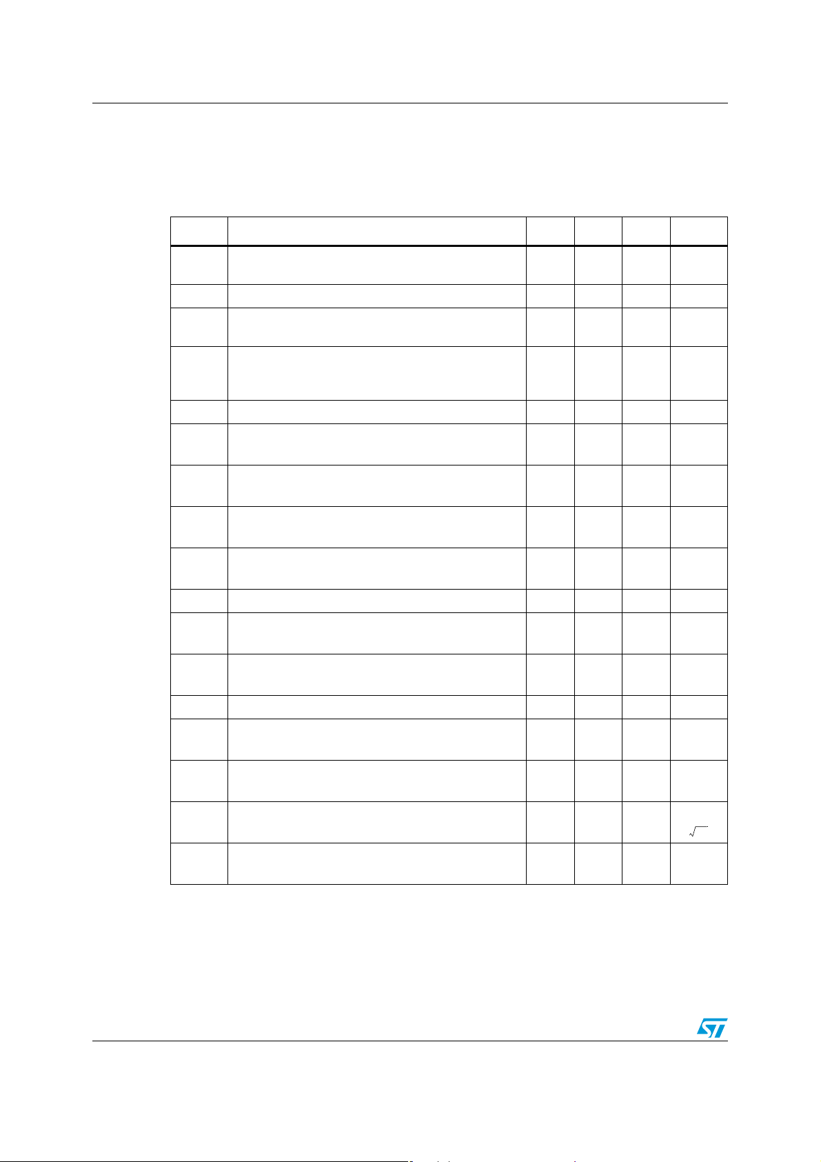
Table 3. VCC = +3 V, V
(unless otherwise specified)
Symbol Parameter Min. Typ. Max. Unit
= 0 V , RL connected to VCC/2, T
DD
amb
= 25° C
V
DV
Input offset voltage
io
io
I
io
I
ib
≤ T
T
min
amb
≤ T
max
Input offset voltage drift 2 µV/°C
Input offset current
≤ T
T
min
amb
≤ T
max
Input bias current
V
= VCC/2
icm
≤ T
T
min
amb
≤ T
max
130
35 100
6
8
80
200
mV
nA
nA
CMR Common mode rejection ratio 50 80 dB
SVR
V
V
GBP
Supply voltage rejection ratio
V
= 2.7 V to 3.3 V 60 80
CC
Large signal voltage gain
A
vd
Vo = 2 V
High level output voltage
OH
RL = 600 Ω
, RL = 600 Ω
pk-pk
2.8 2.9 V
Low level output voltage
OL
RL = 600 Ω
I
Output short-circuit current 10 mA
sc
Supply current (per amplifier)
I
CC
No load, V
= VCC/2
icm
Gain bandwidth product
R
= 2 kΩ
L
80 dB
80 250 mV
0.9 1.3 mA
3MHz
dB
SR Slew rate 1 V/µs
∅m
Gm
THD
Phase margin at unit gain
R
= 600 Ω, CL =100 pF
L
Gain margin
R
= 600 Ω, CL =100 pF
L
Equivalent input noise voltage
e
n
f = 1 kHz
Total harmonic distortion
V
= 4 V
out
pk-pk
, F = 10 kHz, AV = 2, RL =10 kΩ
60 Degrees
10 dB
nV
25
-----------Hz
0.01 %
4/18 Doc ID 5561 Rev 8

TS951, TS952, TS954 Electrical characteristics
Table 4. VCC = +5 V, VDD = 0 V, RL connected to VCC/2, T
amb
= 25° C
(unless otherwise specified)
Symbol Parameter Min. Typ. Max. Unit
V
DV
Input offset voltage
io
T
≤ T
amb
≤ T
max
min
Input offset voltage drift 2 µV/°C
io
6
8
mV
Input offset current
I
io
V
icm
T
min
= VCC/2
≤ T
≤ T
amb
max
130
80
nA
Input bias current
I
ib
V
icm
T
min
= VCC/2
≤ T
≤ T
amb
max
35 100
200
nA
CMR Common mode rejection ratio 50 80 dB
SVR
A
V
V
I
GBP
Supply voltage rejection ratio
VCC = 2.7 V to 3.3 V
Large signal voltage gain
vd
Vo = 2 V
, RL = 600 Ω
pk-pk
High level output voltage
OH
RL = 600 Ω
Low level output voltage
OL
RL = 600 Ω
I
Output short-circuit current 10 mA
sc
Supply current (per amplifier)
CC
No load, V
= VCC/2
icm
Gain bandwidth product
R
= 2 kΩ
L
60 80 dB
86 dB
4.7 4.8 V
80 300 mV
0.95 1.4 mA
3MHz
SR Slew rate 1 V/μs
∅m
Gm
THD
Phase margin at unit gain
R
= 600 Ω, CL =100 pF
L
Gain margin
R
= 600 Ω, CL =100 pF
L
Equivalent input noise voltage
e
n
f = 1 kHz
Total harmonic distortion
V
= 4 V
out
pk-pk
, F = 10 kHz, AV = 2, RL =10 kΩ
60 Degrees
10 dB
nV
25
------------
0.01 %
Hz
Doc ID 5561 Rev 8 5/18

Electrical characteristics TS951, TS952, TS954
Figure 1. Supply current vs. supply voltage Figure 2. Output short circuit current vs.
output voltage
Figure 3. Voltage gain and phase vs.
Figure 4. Supply current vs. temperature
frequency
Figure 5. Output short circuit current vs.
Figure 6. Slew rate vs. temperature
temperature
6/18 Doc ID 5561 Rev 8
 Loading...