


TS951, TS952, TS954
Input/output rail-to-rail low power operational amplifiers
Features
■ Rail-to-rail input common-mode voltage range
■ Rail-to-rail output voltage swing
■ Operating from 2.7 V to 12 V
■ High-speed (3 MHz, 1 V/µs)
■ Low consumption (0.9 mA at 3 V)
■ Supply voltage rejection ratio: 80 dB
■ Latch-up immunity
■ Available in SOT23-5 micropackage
Applications
■ Set-top boxes
■ Laptop/notebook computers
■ Transformer/line drivers
■ Personal entertainment (CD players)
■ Portable communications (cell phones,
pagers)
■ Instrumentation and sensoring
■ Digital-to-analog converter buffers
■ Portable headphone speaker drivers
TS951ILT
TS951ID
TS952IN-TS952ID-TS952IPT
Description
The TS951, TS952 and TS954 family of devices
are rail-to-rail BiCMOS operational amplifiers
optimized and fully specified for 3 V and 5 V
operation.
The TS951 is housed in the space-saving 5-pin
SOT23 package that makes it well-suited for
battery-powered systems. This micropackage
simplifies the PC board design because of its
ability to be placed in tight spaces (outside
dimensions are: 2.8 mm x 2.9 mm).
February 2011 Doc ID 5561 Rev 8 1/18
TS954IN-TS954ID-TS954IPT
www.st.com
18

Absolute maximum ratings and operating conditions TS951, TS952, TS954
1 Absolute maximum ratings and operating conditions
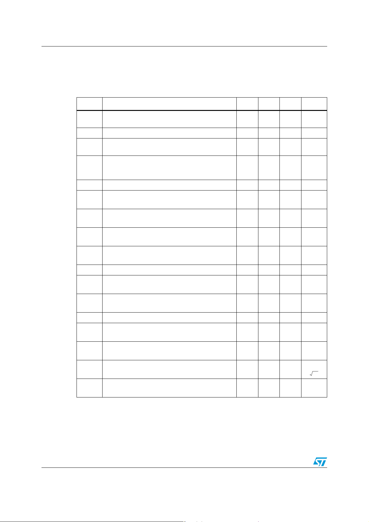
Table 1. Absolute maximum ratings
Symbol Parameter Value Unit
(3)
(1)
(6)
(2)
(5)
14 V
±1 V
VDD-0.3 to VCC+0.3 V
(4)
250
125
103
°C/W
120
100
(4)
81
40
31
°C/W
37
32
1
2
kV
3
100 V
(7)
1.5
1.5
kV
1
V
CC
V
id
V
in
T
stg
T
R
thja
R
thjc
ESD
Supply voltage
Differential input voltage
Input voltage
Storage temperature range -65 to +150
Maximum junction temperature 150 °C
j
Thermal resistance junction to ambient
SOT23-5
SO-8
SO-14
TSSOP8
TSSOP14
Thermal resistance junction to case
SOT23-5
SO-8
SO-14
TSSOP8
TSSOP14
HBM: human body model
TS951
TS952
TS954
MM: machine model
CDM: charged device model
TS951
TS952
TS954
Latch-up immunity 200 mA
Lead temperature (soldering, 10sec) 260 °C
1. All voltage values, except differential voltage are with respect to network ground terminal.
2. Differential voltages are the non-inverting input terminal with respect to the inverting input terminal.
If V
> ±1 V, the maximum input current must not exceed ±1 mA. In this case (Vid > ±1 V), an input series
id
resistor must be added to limit input current.
3. Do not exceed 14 V.
4. Short-circuits can cause excessive heating and destructive dissipation. Rth are typical values.
5. Human body model: a 100 pF capacitor is charged to the specified voltage, then discharged through a
1.5 kΩ resistor between two pins of the device. This is done for all couples of connected pin combinations
while the other pins are floating.
6. Machine model: a 200 pF capacitor is charged to the specified voltage, then discharged directly between
two pins of the device with no external series resistor (internal resistor < 5 Ω). This is done for all couples of
connected pin combinations while the other pins are floating.
7. Charged device model: all pins and the package are charged together to the specified voltage and then
discharged directly to the ground through only one pin. This is done for all pins.
2/18 Doc ID 5561 Rev 8

TS951, TS952, TS954 Absolute maximum ratings and operating conditions
Table 2. Operating conditions
Symbol Parameter Value Unit
V
T
V
CC
icm
oper
Supply voltage 2.7 to 12 V
Common mode input voltage range VDD -0.2 to VCC +0.2 V
Operating free air temperature range -40 to +125 °C
Doc ID 5561 Rev 8 3/18
Electrical characteristics TS951, TS952, TS954
2 Electrical characteristics
Table 3. VCC = +3 V, V
(unless otherwise specified)
Symbol Parameter Min. Typ. Max. Unit
= 0 V , RL connected to VCC/2, T
DD
amb
= 25° C
V
DV
Input offset voltage
io
io
I
io
I
ib
≤ T
T
min
amb
≤ T
max
Input offset voltage drift 2 µV/°C
Input offset current
≤ T
T
min
amb
≤ T
max
Input bias current
V
= VCC/2
icm
≤ T
T
min
amb
≤ T
max
130
35 100
6
8
80
200
mV
nA
nA
CMR Common mode rejection ratio 50 80 dB
SVR
V
V
GBP
Supply voltage rejection ratio
V
= 2.7 V to 3.3 V 60 80
CC
Large signal voltage gain
A
vd
Vo = 2 V
High level output voltage
OH
RL = 600 Ω
, RL = 600 Ω
pk-pk
2.8 2.9 V
Low level output voltage
OL
RL = 600 Ω
I
Output short-circuit current 10 mA
sc
Supply current (per amplifier)
I
CC
No load, V
= VCC/2
icm
Gain bandwidth product
R
= 2 kΩ
L
80 dB
80 250 mV
0.9 1.3 mA
3MHz
dB
SR Slew rate 1 V/µs
∅m
Gm
THD
Phase margin at unit gain
R
= 600 Ω, CL =100 pF
L
Gain margin
R
= 600 Ω, CL =100 pF
L
Equivalent input noise voltage
e
n
f = 1 kHz
Total harmonic distortion
V
= 4 V
out
pk-pk
, F = 10 kHz, AV = 2, RL =10 kΩ
60 Degrees
10 dB
nV
25
-----------Hz
0.01 %
4/18 Doc ID 5561 Rev 8

TS951, TS952, TS954 Electrical characteristics
Table 4. VCC = +5 V, VDD = 0 V, RL connected to VCC/2, T
amb
= 25° C
(unless otherwise specified)
Symbol Parameter Min. Typ. Max. Unit
V
DV
Input offset voltage
io
T
≤ T
amb
≤ T
max
min
Input offset voltage drift 2 µV/°C
io
6
8
mV
Input offset current
I
io
V
icm
T
min
= VCC/2
≤ T
≤ T
amb
max
130
80
nA
Input bias current
I
ib
V
icm
T
min
= VCC/2
≤ T
≤ T
amb
max
35 100
200
nA
CMR Common mode rejection ratio 50 80 dB
SVR
A
V
V
I
GBP
Supply voltage rejection ratio
VCC = 2.7 V to 3.3 V
Large signal voltage gain
vd
Vo = 2 V
, RL = 600 Ω
pk-pk
High level output voltage
OH
RL = 600 Ω
Low level output voltage
OL
RL = 600 Ω
I
Output short-circuit current 10 mA
sc
Supply current (per amplifier)
CC
No load, V
= VCC/2
icm
Gain bandwidth product
R
= 2 kΩ
L
60 80 dB
86 dB
4.7 4.8 V
80 300 mV
0.95 1.4 mA
3MHz
SR Slew rate 1 V/μs
∅m
Gm
THD
Phase margin at unit gain
R
= 600 Ω, CL =100 pF
L
Gain margin
R
= 600 Ω, CL =100 pF
L
Equivalent input noise voltage
e
n
f = 1 kHz
Total harmonic distortion
V
= 4 V
out
pk-pk
, F = 10 kHz, AV = 2, RL =10 kΩ
60 Degrees
10 dB
nV
25
------------
0.01 %
Hz
Doc ID 5561 Rev 8 5/18

Electrical characteristics TS951, TS952, TS954
Figure 1. Supply current vs. supply voltage Figure 2. Output short circuit current vs.
output voltage
Figure 3. Voltage gain and phase vs.
Figure 4. Supply current vs. temperature
frequency
Figure 5. Output short circuit current vs.
Figure 6. Slew rate vs. temperature
temperature
6/18 Doc ID 5561 Rev 8

TS951, TS952, TS954 Electrical characteristics
Figure 7. THD + noise vs. V
Figure 9. THD + noise vs. V
out
out
Figure 8. THD + noise vs. frequency
Figure 10. Equivalent input noise voltage vs.
frequency
Doc ID 5561 Rev 8 7/18

Package information TS951, TS952, TS954
3 Package information
In order to meet environmental requirements, ST offers these devices in different grades of
ECOPACK
specifications, grade definitions and product status are available at: www.st.com.
ECOPACK
®
packages, depending on their level of environmental compliance. ECOPACK®
®
is an ST trademark.
8/18 Doc ID 5561 Rev 8

TS951, TS952, TS954 Package information
3.1 SOT23-5 package information
Figure 11. SOT23-5 package mechanical drawing
Table 5. SOT23-5 package mechanical data
Dimensions
Ref.
Min. Typ. Max. Min. Typ. Max.
A 0.90 1.20 1.45 0.035 0.047 0.057
A1 0.15 0.006
A2 0.90 1.05 1.30 0.035 0.041 0.051
B 0.35 0.40 0.50 0.013 0.015 0.019
C 0.09 0.15 0.20 0.003 0.006 0.008
D 2.80 2.90 3.00 0.110 0.114 0.118
D1 1.90 0.075
e 0.95 0.037
E 2.60 2.80 3.00 0.102 0.110 0.118
F 1.50 1.60 1.75 0.059 0.063 0.069
L 0.10 0.35 0.60 0.004 0.013 0.023
K 0 degrees 10 degrees
Millimeters Inches
Doc ID 5561 Rev 8 9/18

Package information TS951, TS952, TS954
3.2 DIP8 package information
Figure 12. DIP8 package mechanical drawing
Table 6. DIP8 package mechanical data
Dimensions
Ref.
Min. Typ. Max. Min. Typ. Max.
A5.330.210
A1 0.38 0.015
A2 2.92 3.30 4.95 0.115 0.130 0.195
b 0.36 0.46 0.56 0.014 0.018 0.022
b2 1.14 1.52 1.78 0.045 0.060 0.070
c 0.20 0.25 0.36 0.008 0.010 0.014
D 9.02 9.27 10.16 0.355 0.365 0.400
E 7.62 7.87 8.26 0.300 0.310 0.325
E1 6.10 6.35 7.11 0.240 0.250 0.280
e 2.54 0.100
eA 7.62 0.300
eB 10.92 0.430
L 2.92 3.30 3.81 0.115 0.130 0.150
Millimeters Inches
10/18 Doc ID 5561 Rev 8

TS951, TS952, TS954 Package information
3.3 SO-8 package information
Figure 13. SO-8 package mechanical drawing
Table 7. SO-8 package mechanical data
Dimensions
Ref.
Min. Typ. Max. Min. Typ. Max.
A1.750.069
A1 0.10 0.25 0.004 0.010
A2 1.25 0.049
b 0.28 0.48 0.011 0.019
c 0.17 0.23 0.007 0.010
D 4.80 4.90 5.00 0.189 0.193 0.197
E 5.80 6.00 6.20 0.228 0.236 0.244
E1 3.80 3.90 4.00 0.150 0.154 0.157
e 1.27 0.050
h 0.25 0.50 0.010 0.020
L 0.40 1.27 0.016 0.050
L1 1.04 0.040
k1° 8°1° 8°
ccc 0.10 0.004
Millimeters Inches
Doc ID 5561 Rev 8 11/18

Package information TS951, TS952, TS954
3.4 TSSOP8 package information
Figure 14. TSSOP8 package mechanical drawing
Table 8. TSSOP8 package mechanical data
Dimensions
Ref.
Min. Typ. Max. Min. Typ. Max.
A1.200.047
A1 0.05 0.15 0.002 0.006
A2 0.80 1.00 1.05 0.031 0.039 0.041
b 0.19 0.30 0.007 0.012
c 0.09 0.20 0.004 0.008
D 2.90 3.00 3.10 0.114 0.118 0.122
E 6.20 6.40 6.60 0.244 0.252 0.260
E1 4.30 4.40 4.50 0.169 0.173 0.177
e 0.65 0.0256
k0° 8°0° 8°
L 0.45 0.60 0.75 0.018 0.024 0.030
L1 1 0.039
aaa 0.10 0.004
Millimeters Inches
12/18 Doc ID 5561 Rev 8

TS951, TS952, TS954 Package information
3.5 DIP14 package information
Figure 15. DIP14 package mechanical drawing
Table 9. DIP14 package mechanical data
Dimensions
Millimeters Inches
Ref.
Min. Typ. Max. Min. Typ. Max.
A5.330.21
A1 0.38 0.015
A2 2.92 3.30 4.95 0.11 0.13 0.19
b 0.36 0.46 0.56 0.014 0.018 0.022
b2 1.14 1.52 1.78 0.04 0.06 0.07
c 0.20 0.25 0.36 0.007 0.009 0.01
D 18.67 19.05 19.69 0.73 0.75 0.77
E 7.62 7.87 8.26 0.30 0.31 0.32
E1 6.10 6.35 7.11 0.24 0.25 0.28
e2.54 0.10
e1 15.24 0.60
eA 7.62 0.30
eB 10.92 0.43
L 2.92 3.30 3.81 0.11 0.13 0.15
Doc ID 5561 Rev 8 13/18

Package information TS951, TS952, TS954
3.6 SO-14 package information
Figure 16. SO-14 package mechanical drawing
Table 10. SO-14 package mechanical data
Dimensions
Millimeters Inches
Ref.
Min. Typ. Max. Min. Typ. Max.
A 1.35 1.75 0.05 0.068
A1 0.10 0.25 0.004 0.009
A2 1.10 1.65 0.04 0.06
B 0.33 0.51 0.01 0.02
C 0.19 0.25 0.007 0.009
D 8.55 8.75 0.33 0.34
E 3.80 4.0 0.15 0.15
e1.27 0.05
H 5.80 6.20 0.22 0.24
h 0.25 0.50 0.009 0.02
L 0.40 1.27 0.015 0.05
k 8° (max.)
ddd 0.10 0.004
14/18 Doc ID 5561 Rev 8

TS951, TS952, TS954 Package information
3.7 TSSOP14 package information
Figure 17. TSSOP14 package mechanical drawing
Table 11. TSSOP14 package mechanical data
Dimensions
Ref.
Min. Typ. Max. Min. Typ. Max.
A1.200.047
A1 0.05 0.15 0.002 0.004 0.006
A2 0.80 1.00 1.05 0.031 0.039 0.041
b 0.19 0.30 0.007 0.012
c 0.09 0.20 0.004 0.0089
D 4.90 5.00 5.10 0.193 0.197 0.201
E 6.20 6.40 6.60 0.244 0.252 0.260
E1 4.30 4.40 4.50 0.169 0.173 0.176
e 0.65 0.0256
L 0.45 0.60 0.75 0.018 0.024 0.030
L1 1.00 0.039
k0° 8°0° 8°
aaa 0.10 0.004
Millimeters Inches
Doc ID 5561 Rev 8 15/18

Ordering information TS951, TS952, TS954
4 Ordering information
(1)
Temperature
range
Package Packing Marking
SO-8
Tub e o r
Tape & reel
951I
K101
SOT23-5L
(Automotive grade)
Tape & reel
K1A2
Table 12. Order codes
Order code
TS951ID
TS951IDT
TS951ILT SOT23-5L
TS951IYLT
TS952IN DIP8 Tube TS952IN
TS952ID
TS952IDT
TS952IYD
TS952IYDT
TS952IPT TSSOP8
TS952IYPT
(1)
(1)
-40°C to +125°C
(2)
SO-8
SO-8
(Automotive grade)
TSSOP8
(Automotive grade)
Tub e o r
952I
Tape & reel
952IY
952I
Tape & reel
952Y
TS954IN DIP14 Tube TS954IN
TS954ID
TS954IDT
TS954IYD
TS954IYDT
(1)
(1)
TS954IPT TSSOP14
TS954IYPT
(2)
SO-14
SO-14
(Automotive grade)
TSSOP14
(Automotive grade)
Tub e o r
954I
Tape & reel
954IY
954I
Tape & reel
954Y
1. Qualified and characterized according to AEC Q100 and Q003 or equivalent, advanced screening according to AEC Q001
& Q 002 or equivalent.
2. Qualification and characterization according to AEC Q100 and Q003 or equivalent, advanced screening according to AEC
Q001 & Q 002 or equivalent are on-going.
16/18 Doc ID 5561 Rev 8

TS951, TS952, TS954 Revision history
5 Revision history
Table 13. Document revision history
Date Revision Changes
01-May-2001 1 Initial release.
02-Jan-2005 2
03-Jul-2005 3
04-Aug-2005 4 Table data was badly formatted, see Table 4 on page 5.
15-Dec-2005 5 TS951IYLT PPAP reference added, see Table 12: Order codes.
10-Dec-2007 6
10-Mar-2009 7 Removed TS951IN and TS951IYD/DT from Table 12: Order codes.
24-Feb-2011 8
Modifications on AMR Table 1 on page 2 (explanation of Vid and Vi
limits, ESD MM and CDM values added, R
PPAP references inserted in the datasheet see Table 12: Order
codes.
Added missing order codes, and automotive grade status in
Table 12: Order codes.
Updated footnotes for ESD parameters in Table 1: Absolute
maximum ratings.
Reformatted package information.
Changed TS951IYLT marking and updated automotive grade status
in Table 12: Order codes.
added).
thja
Doc ID 5561 Rev 8 17/18

TS951, TS952, TS954
Please Read Carefully:
Information in this document is provided solely in connection with ST products. STMicroelectronics NV and its subsidiaries (“ST”) reserve the
right to make changes, corrections, modifications or improvements, to this document, and the products and services described herein at any
time, without notice.
All ST products are sold pursuant to ST’s terms and conditions of sale.
Purchasers are solely responsible for the choice, selection and use of the ST products and services described herein, and ST assumes no
liability whatsoever relating to the choice, selection or use of the ST products and services described herein.
No license, express or implied, by estoppel or otherwise, to any intellectual property rights is granted under this document. If any part of this
document refers to any third party products or services it shall not be deemed a license grant by ST for the use of such third party products
or services, or any intellectual property contained therein or considered as a warranty covering the use in any manner whatsoever of such
third party products or services or any intellectual property contained therein.
UNLESS OTHERWISE SET FORTH IN ST’S TERMS AND CONDITIONS OF SALE ST DISCLAIMS ANY EXPRESS OR IMPLIED
WARRANTY WITH RESPECT TO THE USE AND/OR SALE OF ST PRODUCTS INCLUDING WITHOUT LIMITATION IMPLIED
WARRANTIES OF MERCHANTABILITY, FITNESS FOR A PARTICULAR PURPOSE (AND THEIR EQUIVALENTS UNDER THE LAWS
OF ANY JURISDICTION), OR INFRINGEMENT OF ANY PATENT, COPYRIGHT OR OTHER INTELLECTUAL PROPERTY RIGHT.
UNLESS EXPRESSLY APPROVED IN WRITING BY AN AUTHORIZED ST REPRESENTATIVE, ST PRODUCTS ARE NOT
RECOMMENDED, AUTHORIZED OR WARRANTED FOR USE IN MILITARY, AIR CRAFT, SPACE, LIFE SAVING, OR LIFE SUSTAINING
APPLICATIONS, NOR IN PRODUCTS OR SYSTEMS WHERE FAILURE OR MALFUNCTION MAY RESULT IN PERSONAL INJURY,
DEATH, OR SEVERE PROPERTY OR ENVIRONMENTAL DAMAGE. ST PRODUCTS WHICH ARE NOT SPECIFIED AS "AUTOMOTIVE
GRADE" MAY ONLY BE USED IN AUTOMOTIVE APPLICATIONS AT USER’S OWN RISK.
Resale of ST products with provisions different from the statements and/or technical features set forth in this document shall immediately void
any warranty granted by ST for the ST product or service described herein and shall not create or extend in any manner whatsoever, any
liability of ST.
ST and the ST logo are trademarks or registered trademarks of ST in various countries.
Information in this document supersedes and replaces all information previously supplied.
The ST logo is a registered trademark of STMicroelectronics. All other names are the property of their respective owners.
© 2011 STMicroelectronics - All rights reserved
STMicroelectronics group of companies
Australia - Belgium - Brazil - Canada - China - Czech Republic - Finland - France - Germany - Hong Kong - India - Israel - Italy - Japan -
Malaysia - Malta - Morocco - Philippines - Singapore - Spain - Sweden - Switzerland - United Kingdom - United States of America
www.st.com
18/18 Doc ID 5561 Rev 8
 Loading...