

ST TS941, TS942, TS944, TS941A, TS942A User Manual
...
TS94x, TS94xA, TS94xB
Output rail-to-rail micropower operational amplifiers
Features
■ Rail-to-rail output voltage swing
■ Micropower consumption (1.2 µA)
■ Single supply operation (2.5 V to 10 V)
■ CMOS inputs
■ Ultra low input bias current (1 pA)
■ ESD protection (2 kV)
■ Latch-up immunity (class A)
■ Available in SOT23-5 micropackage
Applications
■ Battery-powered systems (alarm)
■ Portable communication systems (pagers)
■ Smoke/gas/fire detectors
■ Instrumentation and sensoring
■ PH meter
Description
The TS94x (single, dual and quad) series are
operational amplifiers characterized for 2.5 V to
10 V operation over a -40° C to +85° C
temperature range.
They exhibit excellent consumption -1.2 µA, while
featuring 10 kHz gain bandwidth product, 1.5 mA
output capability and output rail-to-rail operation
- 2.85 V typical at 3 V with R
The TS94x op-amps are ideal for battery-powered
systems, where very low supply current and
output rail-to-rail are required. Their very low
- 1 pA typical input bias current and constant
supply current over supply voltage enhance the
devices’ performance near the end of the battery
charge or battery life.
=10 kΩ.
L
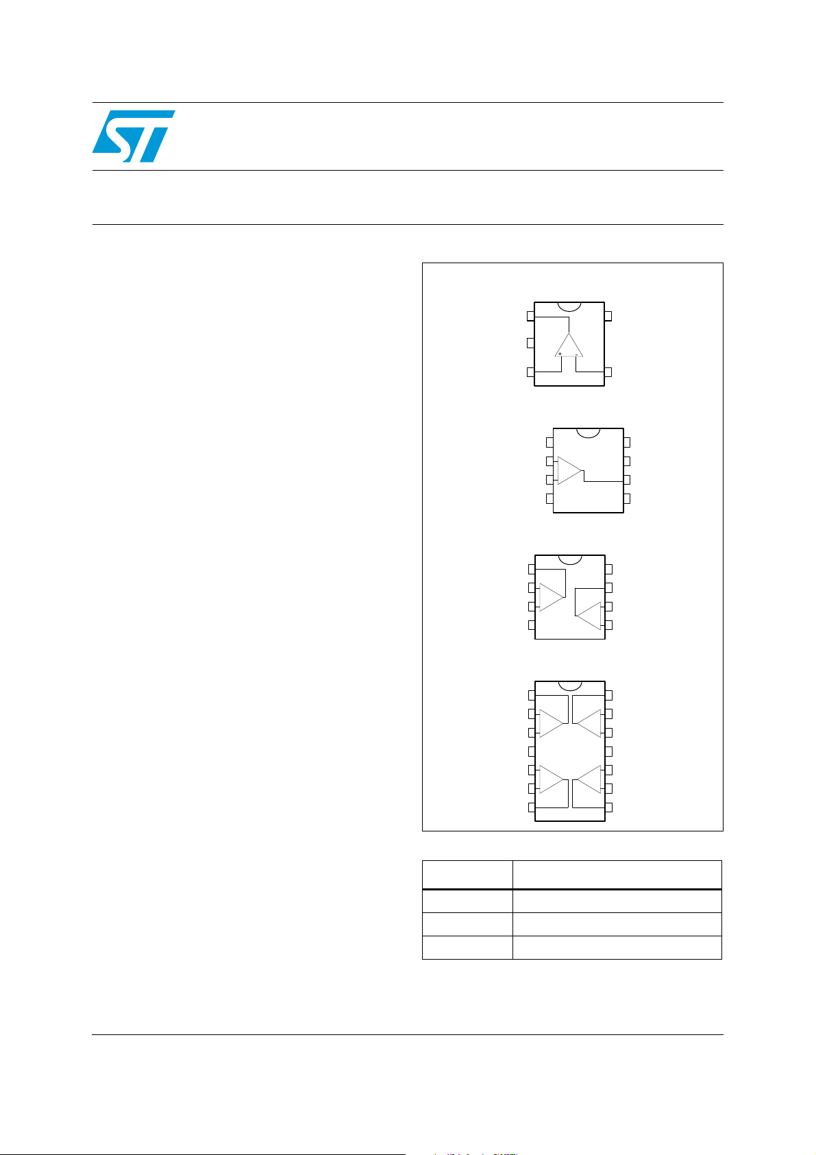
TS941ILT
Output
Non-inverting input
1
V
2
DD
3
V
5
CC
Inverting input
4
TS941ID-TS941IDT
N.C.
N.C.
Inverting Input 1
Non-inverting Input 1
V
1
2
-
+
3
4
DD
8
V
7
6
Output 2
N.C.
5
CC
TS942ID-TS942IDT-TS942IPT
Output 1
Inverting Input 1
Non-inverting Input 1
V
1
-
2
+
3
45
DD
V
8
CC
Output 2
7
-
Inverting Input 2
6
+
Non-inverting Input 2
TS944ID-TS944IDT-TS944IPT
Output 4
Output 1
1
Inverting Input 1
Non-inverting Input 1
Non-inverting Input 2
Inverting Input 2
Table 1. Device summary
V
Output 2
2
-
+
3
4
CC
5
+
-
6
7
Reference Selection on offset voltage
TS94x TS941, TS942, TS944
TS94xA TS941A, TS942A, TS944A
14
13
-
+
12
11
10
+
-
9
8
Inverting Input 4
Non-inverting Input 4
V
DD
Non-inverting Input 3
Inverting Input 3
Output 3
TS94xB TS941B, TS942B, TS944B
October 2009 Doc ID 6972 Rev 6 1/18
www.st.com
18
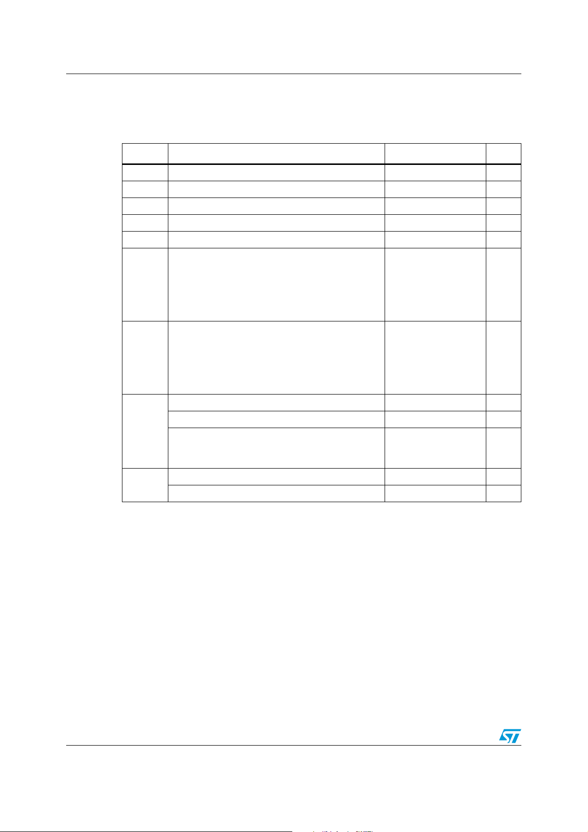
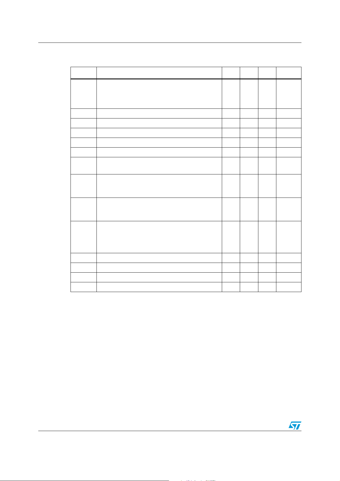
Absolute maximum ratings and operating conditions TS94x, TS94xA, TS94xB
1 Absolute maximum ratings and operating conditions
Table 2. Absolute maximum ratings
Symbol Parameter Value Unit
V
CC
V
id
V
in
T
stg
T
R
thja
R
thjc
ESD
Supply voltage
Differential input voltage
Input voltage range
Storage temperature range -65 to +150 °C
Maximum junction temperature 150 °C
j
Thermal resistance junction to ambient
SOT23-5
SO-8
SO-14
TSSOP8
TSSOP14
Thermal resistance junction to case
SOT23-5
SO-8
SO-14
TSSOP8
TSSOP14
HBM: human body model
MM: machine model
CDM: charged device model
TS941 - TS944IDT
TS942 - TS944IPT
Latch-up immunity 200 mA
Lead temperature (soldering, 10sec) 250 °C
(1)
(2)
(3)
(5)
(6)
(TS941, TS942)
(7)
(4)
12 V
± V
CC
V
VDD-0.3 to VCC+0.3 V
(4)
250
125
103
°C/W
120
100
81
40
31
°C/W
37
32
2kV
200 V
1.5
kV
1
1. All voltage values, except differential voltage are with respect to network terminal.
2. Differential voltages are the non-inverting input terminal with respect to the inverting input terminal.
3. The magnitude of input and output voltages must never exceed VCC +0.3 V.
4. Short-circuits can cause excessive heating and destructive dissipation. Rth are typical values.
5. Human body model: a 100 pF capacitor is charged to the specified voltage, then discharged through a
1.5 kΩ resistor between two pins of the device. This is done for all couples of connected pin combinations
while the other pins are floating.
6. Machine model: a 200 pF capacitor is charged to the specified voltage, then discharged directly between
two pins of the device with no external series resistor (internal resistor < 5 Ω). This is done for all couples of
connected pin combinations while the other pins are floating.
7. Charged device model: all pins and the package are charged together to the specified voltage and then
discharged directly to the ground through only one pin. This is done for all pins.
2/18 Doc ID 6972 Rev 6

TS94x, TS94xA, TS94xB Absolute maximum ratings and operating conditions
Table 3. Operating conditions
Symbol Parameter Value Unit
V
V
T
CC
icm
oper
Supply voltage 2.5 to 10 V
Common mode input voltage range VDD -0.2 to VCC -1.3 V
Operating free air temperature range -40 to + 85 °C
Doc ID 6972 Rev 6 3/18
Electrical characteristics TS94x, TS94xA, TS94xB
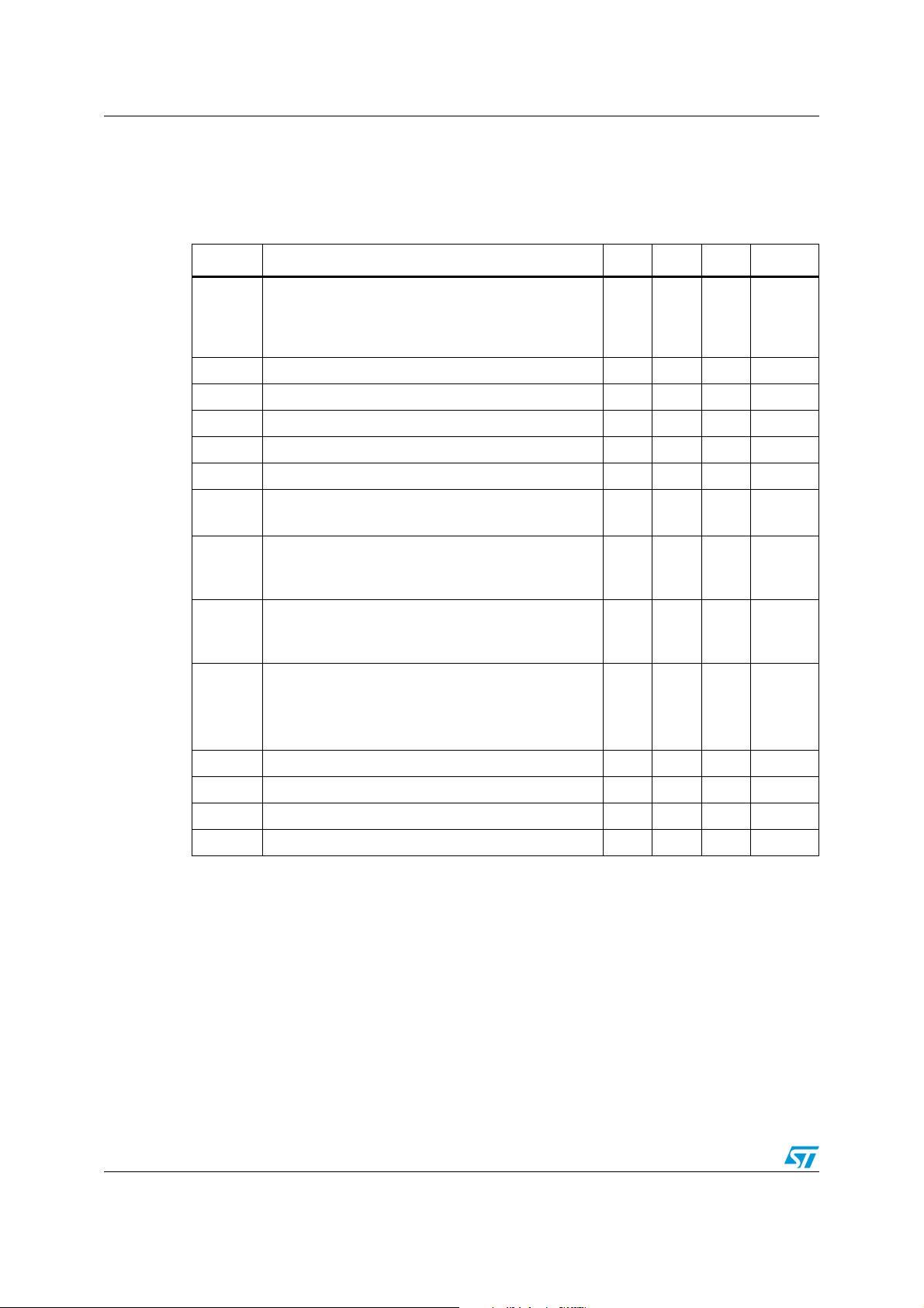
2 Electrical characteristics
Table 4. VCC = +2.5 V, VDD = 0 V, RL connected to VCC/2, T
(unless otherwise specified)
Symbol Parameter Min. Typ. Max. Unit
Input offset voltage
V
io
ΔV
io
I
io
I
ib
CMR Common mode rejection ratio 60 85 dB
SVR Supply voltage rejection ratio 50 78 dB
TS941/2/4
TS941/2/4A
TS941/2/4B
Input offset voltage drift 7 µV/°C
Input offset current
Input bias current
(1)
(1)
= 25° C
amb
1 100 pA
1 150 pA
10
5
mV
2
A
Large signal voltage gain
vd
= 2 Vpp, RL = 1 MΩ
V
O
High level output voltage
V
OH
= 100 mV, RL = 1 MΩ
V
ID
RL = 10 kΩ
Low level output voltage
V
OL
= -100 mV, RL = 1 MΩ
V
ID
RL = 10 kΩ
Output source current
VID = 100 mV, VO = V
Output sink current
= -100 mV, VO = V
V
ID
Supply current (per amplifier), A
I
I
CC
o
GBP Gain bandwidth product, R
SR Slew rate, R
= 1 MΩ, CL = 50 pF 3 4.5 V/ms
L
φm Phase margin, C
1. Maximum values include unavoidable inaccuracies of the industrial tests.
DD
CC
= 1, no load 1.2 1.8 µA
VCL
= 1 MΩ, CL = 50 pF 10 kHz
L
= 50 pF 65 Degrees
L
2.45
2.3
350
280
100 dB
2.49
2.4
1
mV
1005200
650
µA
500
V
4/18 Doc ID 6972 Rev 6
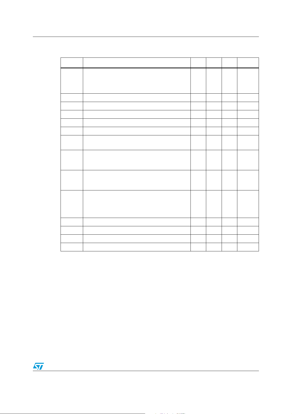
TS94x, TS94xA, TS94xB Electrical characteristics
Table 5. VCC = +3 V, VDD = 0 V, RL connected to VCC/2,T
(unless otherwise specified)
(1)
Symbol Parameter Min. Typ. Max. Unit
Input offset voltage
V
io
TS941/2/4
TS941/2/4A
TS941/2/4B
ΔV
I
I
Input offset voltage drift 7 µV/°C
io
Input offset current
io
Input bias current
ib
(2)
(2)
CMR Common mode rejection ratio 60 85 dB
SVR Supply voltage rejection ratio 50 85 dB
A
Large signal voltage gain
vd
= 2 Vpp,RL = 1 MΩ
V
O
High level output voltage
V
OH
= 100 mV, RL = 1 MΩ
V
ID
RL = 10 kΩ
Low level output voltage
V
OL
VID = -100 mV, RL = 1 MΩ
= 10 kΩ
R
L
Output source current
= 100 mV, VO = V
V
ID
Output sink current
= -100 mV, VO = V
V
ID
Supply current (per amplifier), A
I
I
CC
o
GBP Gain bandwidth product, R
SR Slew rate, R
= 1 MΩ, CL = 50 pF 3 4.5 V/ms
L
φm Phase margin, C
1. All electrical values are guaranteed with correlation measurements at 2.5 V and 5 V.
2. Maximum values include unavoidable inaccuracies of the industrial tests.
DD
CC
= 1, no load 1.2 1.8 µA
VCL
= 1 MΩ, CL = 50 pF 10 kHz
L
= 50 pF 65 Degrees
L
amb
2.9
2.8
680
650
= 25° C
10
5
2
1 100 pA
1 150 pA
100 dB
2.99
2.85
1
1005200
1500
1300
mV
V
mV
µA
Doc ID 6972 Rev 6 5/18
Electrical characteristics TS94x, TS94xA, TS94xB
Table 6. VCC = +5 V, VDD = 0 V, RL connected to VCC/2, T
amb
= 25° C
(unless otherwise specified)
Symbol Parameter Min. Typ. Max. Unit
Input offset voltage
V
io
TS941/2/4
TS941/2/4A
TS941/2/4B
ΔV
I
I
Input offset voltage drift 7 µV/°C
io
Input offset current
io
Input bias current
ib
(1)
(1)
CMR Common mode rejection ratio 60 85 dB
SVR Supply voltage rejection ratio 50 85 dB
A
Large signal voltage gain
vd
= 2 Vpp, RL = 1 MΩ
V
O
100 dB
High level output voltage
V
OH
= 100 mV, RL = 1 MΩ
V
ID
RL = 10 kΩ
4.9
4.8
4.99
4.85
Low level output voltage
V
OL
VID = -100 mV, RL = 1 MΩ
= 10 kΩ
R
L
1005150
Output source current
= 100 mV, VO = V
V
ID
Output sink current
= -100 mV, VO = V
V
ID
Supply current (per amplifier), A
I
I
CC
o
GBP Gain bandwidth product, R
SR Slew rate, R
= 1 MΩ, CL = 50 pF 3 4.5 V/ms
L
φm Phase margin, C
1. Maximum values include unavoidable inaccuracies of the industrial tests.
DD
CC
= 1, no load 1.2 1.85 µA
VCL
= 1 MΩ, CL = 50 pF 10 kHz
L
= 50 pF 65 Degrees
L
3
3.7
4.5
10
5
mV
2
1 100 pA
1 150 pA
V
1
mV
mA
5
6/18 Doc ID 6972 Rev 6
 Loading...