


TS922
Rail-to-Rail High Output Current Dual Operational Amplifier
■ Rail-to-rail input and output
■ Low noise: 9nV/
√Hz
■ Low distortion
■ High output current: 80mA
(able to drive 32Ω loads)
■ High-speed: 4MHz, 1V/µs
■ Operating from 2.7V to 12V
■ Low input offset voltage: 900µV max
(TS922A)
■ ESD Internal protection: 2kV
■ Latch-up immunity
■ Macromodel included in this specification
■ Dual version available in flip-chip package
Description
The TS922 is a rail-to-rail dual BiCMOS
operational amplifier optimized and fully specified
for 3V and 5V operation.
The device’s high output current allows low-load
impedances to be driven.
Very low noise, low distortion, low offset and a
high output current capability make this device an
excellent choice for high quality, low voltage or
battery operated audio systems.
The device is stable for capacitive loads up to
500pF.
J
TS922IJ
(Flip-chip)
N
DIP-8
(Plastic Package)
D
SO-8
(Plastic Micropackage)
P
TSSOP8
(Thin Shrink Small Outline Package)
Applications
■ Headphone amplifier
■ Piezoelectric speaker driver
■ Sound cards, multimedia systems
■ Line driver, actuator driver
■ Servo amplifier
■ Mobile phone and portable equipment
■ Instrumentation with low noise as key
factor
Order Codes
Part Number Temperature Range Package Packaging
TS922IN/AIN
TS922ID/IDT/AID/AIDT SO Tube or Tape & Reel
TS922IPT/TS922AIPT
TS922IJT Flip-Chip Tape & Reel
May 2005 Revision 3 1/16
-40°C, +125°C
(Thin Shrink Outline Package)
DIP Tube
TSSOP
Tape & Reel
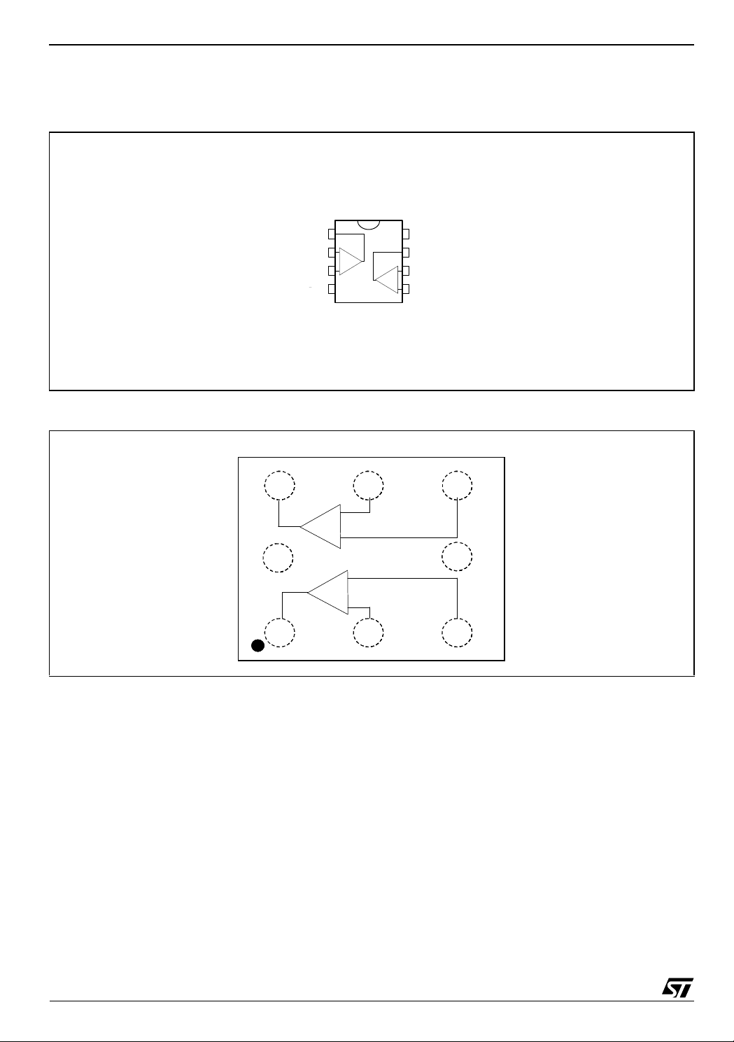
TS922 Pin Diagrams
1 Pin Diagrams
Figure 1: Pin connections (top view)
Output 1
Inverting Input 1
Non-inverting Input 1
1
2
-
+
3
V
45
CC
Figure 2: Pin-out for flip-chip package (top view)
OUT2 -IN2 +IN2
OUT2 -IN2 +IN2
-
-
+
+
VCC+
VCC+
+
+
-
-
V
8
Output 2
7
-
Inverting Input 2
6
+
Non-inverting Input 2
CC
+
GND
GND
+IN1-IN1OUT1
+IN1-IN1OUT1
2/16

Absolute Maximum Ratings TS922
2 Absolute Maximum Ratings
Table 1: Key parameters and their absolute maximum ratings
Symbol Parameter Value Unit
V
T
Supply voltage
CC
V
Differential Input Voltage
id
V
Input Voltage
in
Storage Temperature
stg
Thermal Resistance Junction to Ambient
SO8
R
TSSOP8 120
thja
DIP8 85
Flip Chip 90
T
Maximum Junction Temperature
j
HBM: Human Body Model
ESD
MM: Machine Model
CDM: Charged Device Model 1.5 kV
Output Short Circuit Duration
Latch-up Immunity 200 mA
Soldering Temperature (10sec), leaded version 250 °C
Soldering Temperature (10sec), unleaded version 260 °C
1) All voltages values, except differential voltage are with respect to network ground terminal.
2) Differential voltages are the non-inverting input terminal with respect to the inverting input terminal. If Vid > ±1V, the maximum input current must not exceed ±1mA. In this case (Vid > ±1V) an input serie resistor must be added to limit input current.
3) Do not exceed 14V.
4) Human body model, 100pF discharged through a 1.5kΩ resistor into pin of device.
5) Machine model ESD, a 200pF cap is charged to the specified voltage, then discharged directly into the IC with no external series resistor
(internal resistor < 5
6) There is no short-circuit protection inside the device: short-circuits from the output to V
output current is approximately 80mA, independent of the magnitude of V
circuits on all amplifiers.
1
2
3
4
5
Ω), into pin to pin of device.
14 V
±1 V
VDD-0.3 to VCC+0.3
-65 to +150 °C
125
150 °C
2kV
100 V
see note
can cause excessive heating. The maximum
. Destructive dissipation can result from simultaneous short-
cc
cc
6
V
°C/W
Table 2: Operating conditions
Symbol Parameter Value Unit
V
V
T
Supply voltage
CC
Common Mode Input Voltage Range
icm
Operating Free Air Temperature Range
oper
2.7 to 12 V
-0.2 to VCC +0.2
V
DD
-40 to +125 °C
V
3/16

TS922 Electrical Characteristics
3 Electrical Characteristics
Table 3: VCC = +3V, VDD = 0V, V
= VCC/2, T
icm
= 25°C, RL connected to Vcc/2 (unless otherwise
amb
specified)
Symbol Parameter Min. Typ. Max. Unit
Input Offset Voltage TS922
Input Offset voltage TS922A
Input Offset Voltage TS922IJ (Flip Chip)
V
io
T
≤ T
≤ T
TS922
max.
≤ T
TS922A
max.
≤ T
TS922IJ (Flip Chip)
max.
2
130nA
15 100 nA
DV
min.
min.
min.
≤ T
≤ T
amb
amb
amb
T
T
Input Offset Voltage Drift
io
Input Offset Current
I
io
Vout = Vcc/2
Input Bias Current
I
ib
Vout = Vcc/2
High Level Output Voltage
R
= 10k
V
OH
L
R
= 600Ω
L
RL = 32Ω
2.90
2.87
2.63
Low Level Output Voltage
R
= 10k
V
OL
A
I
cc
GBP
L
R
= 600Ω
L
RL = 32Ω
Large Signal Voltage Gain (V
R
= 10k
L
vd
R
= 600Ω
L
RL = 32Ω
Total Supply Current
no load, V
out
= V
Gain Bandwidth Product
(R
= 600Ω)
L
cc/2
= 2Vpk-pk)
out
180
200
35
16
23mA
4MHz
CMR Common Mode Rejection Ratio 60 80 dB
SVR
Supply Voltage Rejection Ratio
= 2.7 to 3.3V
V
cc
I
Output Short Circuit Current
o
60 85
50 80 mA
SR Slew Rate 0.7 1.3 V/
Phase Margin at Unit Gain
φm
G
m
e
n
THD
C
s
= 600Ω, CL =100pF
R
L
Gain Margin
R
= 600Ω, CL =100pF
L
Equivalent Input Noise Voltage
f = 1kHz
Total Harmonic Distortion
= 2Vpk-pk, F = 1kHz, Av = 1, RL =600Ω
V
out
Channel Separation
68 Degrees
12 dB
9
0.005 %
120 dB
3
0.9
1.5
5
1.8
2.5
µV/°C
50
100
mV
V
mV
V/mV
dB
µs
nV
-----------Hz
4/16

Electrical Characteristics TS922
Table 4: Electrical characteristics VCC = 5V, V
to V
/2 (unless otherwise specified)
cc
= 0V, V
DD
= Vcc/2, T
icm
= 25°C, RL connected
amb
Symbol Parameter Min. Typ. Max. Unit
V
V
DV
V
Input Offset Voltage TS922
Input Offset voltage TS922A
Input Offset Voltage TS922IJ (Flip Chip)
io
T
≤ T
≤ T
min.
amb
max.
TS922
TS922A
TS922IJ (Flip Chip)
Input Offset Voltage TS922IJ (flip chip)
io
T
≤ T
≤ T
min.
amb
Input Offset Voltage Drift
io
Input Offset Current
I
io
Vout = Vcc/2
Input Bias Current
I
ib
Vout = Vcc/2
TS922IJ
max.
High Level Output Voltage
R
= 10k
OH
L
R
= 600Ω
L
RL = 32Ω
2
130nA
15 100 nA
4.90
4.85
4.4
3
0.9
1.5
5
1.8
2.5
1.5
2.5
µV/°C
Low Level Output Voltage
V
OL
A
vd
I
cc
GBP
= 10k
L
R
= 600Ω
L
RL = 32Ω
Large Signal Voltage Gain (V
RL= 10k
R
= 600Ω
L
RL = 32Ω
Total Supply Current
no load, V
out
= V
cc/2
Gain Bandwidth Product
(R
= 600Ω)
L
= 2Vpk-pk)
out
300
200
35
16
23mA
4MHz
50
120
R
CMR Common Mode Rejection Ratio 60 80 dB
SVR
Supply Voltage Rejection Ratio
= 4.5 to 5.5V
V
cc
I
Output Short Circuit Current
o
60 85 dB
50 80 mA
SR Slew Rate 0.7 1.3 V/
φm
G
THD
Phase Margin at Unit Gain
= 600Ω, CL =100pF
R
L
Gain Margin
m
R
= 600Ω, CL =100pF
L
Equivalent Input Noise Voltage
e
n
f = 1kHz
Total Harmonic Distortion
V
= 2Vpk-pk, F = 1kHz, Av = 1, RL =600Ω
out
C
Channel Separation
s
68 Degrees
12 dB
9
0.005 %
120 dB
mV
mV
V
mV
V/mV
µs
nV
-----------Hz
5/16

TS922 Electrical Characteristics
Table 5: Electrical characteristics for V
= 3V, V
CC
= 0V, RL, CL connected to VCC/2, T
DD
amb
(unless otherwise specified)
Symbol Conditions Value Unit
V
A
I
CC
V
icm
V
OH
V
OL
I
sink
I
source
GBP
SR
φm
io
vd
RL = 10kΩ
No load, per operator
RL = 10kΩ
RL = 10kΩ
VO = 3V
VO = 0V
R
= 600kΩ
L
R
= 10kΩ, CL = 100pF
L
R
= 600kΩ
L
0mV
200 V/mV
1.2 mA
-0.2 to 3.2 V
2.95 V
25 mV
80 mA
80 mA
4MHz
1.3 V/
68 Degrees
= 25°C
µs
6/16
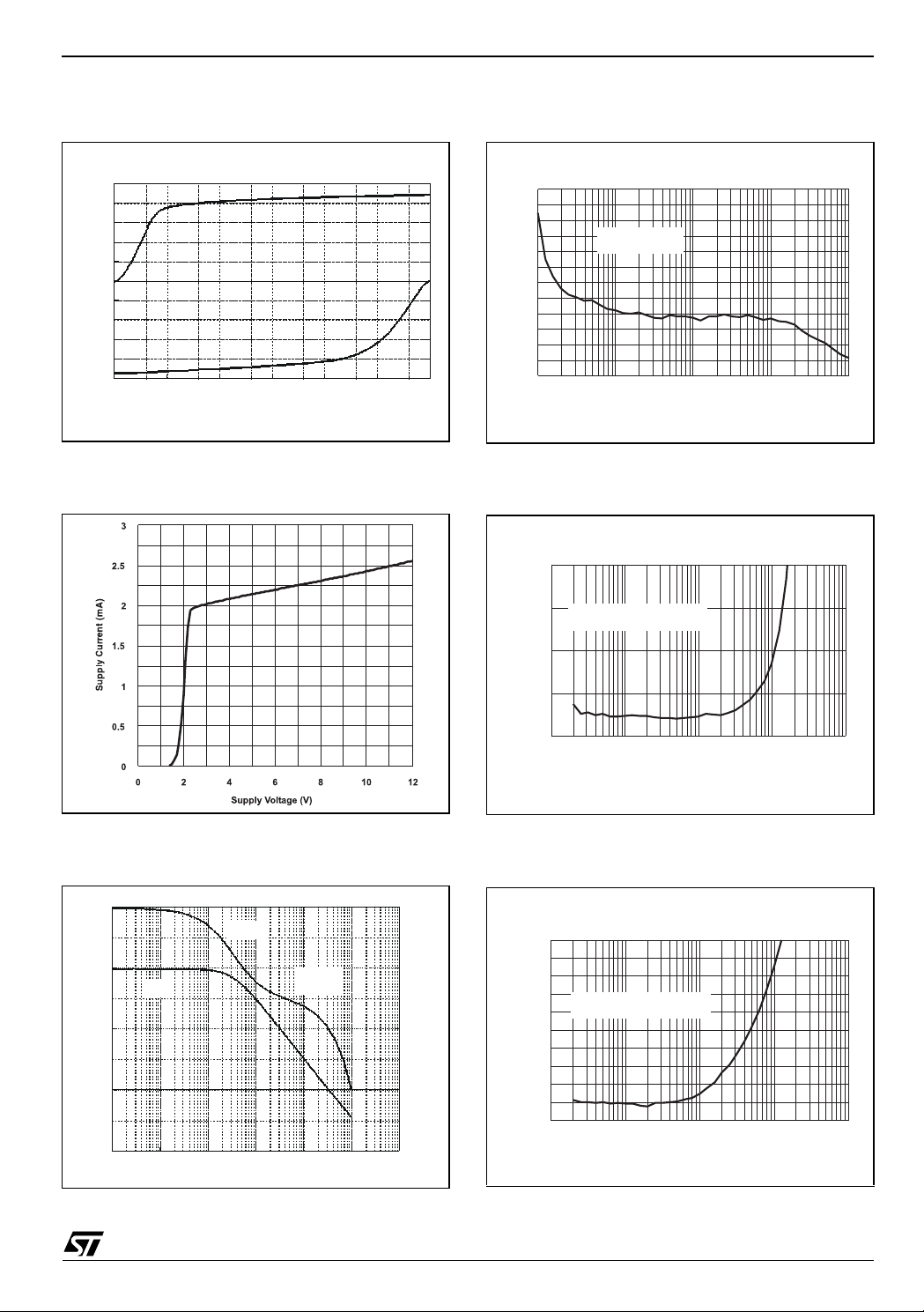
Electrical Characteristics TS922
3
O
Sh
Ci
i
C
(
A)
60
180
Figure 3: Output Short Circuit Current vs.
Output Voltage
100
80
60
m
40
urrent
20
t
0
rcu
-20
ort-
-40
utput
-60
-80
-100
00,511,522,5
Sink
Vcc=0/3V
Source
Output Voltage (V)
Figure 4: Total supply current vs. Supply
voltage
Figure 6: Equivalent Input Noise Voltage vs.
Frequency
30
25
20
15
10
5
Equivalent Input Noise (nV/sqrt(Hz)
0
0.01 0.1 1 10 100
VCC=±1.5V
R
=100Ω
L
Frequency (kHz)
Figure 7: THD + Noise vs. Frequency
0.02
0.015
0.01
THD+Noise (%)
0.005
RL=2k Vo=10Vpp
V
=±6V A v= 1
CC
0
Figure 5: Voltage Gain And Phase vs.
0.01 0.1 1 10 100
Figure 8: THD + Noise vs. Frequency
Frequency (kHz)
Frequency
phase
40
gain
20
Gain ( dB)
0
-20
1E+02 1E+03 1E+04 1E +05 1E+06 1E+07 1E+08
Frequency (Hz)
Rl=10k
Cl=100pF
120
60
Phase (Deg )
0
-60
0.04
0.032
RL=32Ω Vo=4Vpp
0.024
0.016
THD+Noise (%)
0.008
0
VCC=±2.5V Av= 1
0.01 0.1 1 10 100
Frequency (kHz)
7/16
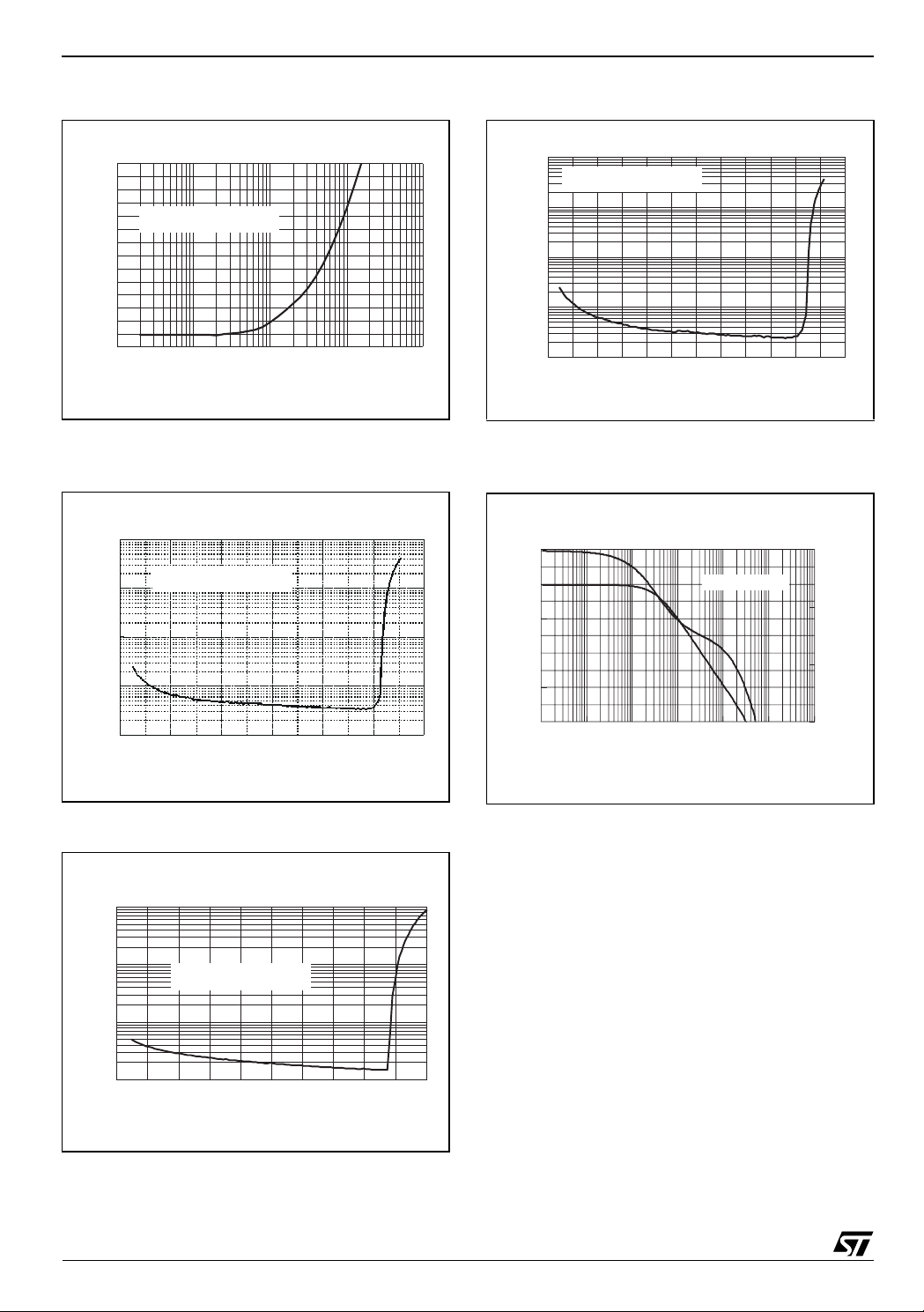
TS922 Electrical Characteristics
2
)
Figure 9: THD + Noise vs. Frequency
0.7
0.6
0.5
0.4
0.3
THD+Noise (%)
0.2
0.1
0
RL=32Ω Vo=2Vpp
VCC=±1.5V Av= 10
0.01 0.1 1 10 100
Frequency (kHz)
Figure 10: THD + Noise vs. Output Voltage
10,000
RL=600Ω f=1kHz
V
=0/3V Av= -1
1,000
0,100
THD+Noise (%)
0,010
CC
Figure 12: THD + Noise vs. Output Voltage
10
0.1
THD+Noise (%)
0.01
0.001
RL=2kΩ f=1kHz
V
=±1.5V Av= -1
CC
1
0 0.2 0.4 0.6 0.8 1 1.2
Vout (Vrms)
Figure 13: Open Loop Gain And Phase vs.
Frequency
50
40
30
Gain(dB)
20
10
CL=500pF
180
120
60
Phase (Deg)
0,001
0 0,2 0,4 0,6 0,8 1 1,
Vout (Vrms
Figure 11: THD + Noise vs. Output Voltage
10
1
THD+Noise (%)
0.1
0.01
0 0.2 0.4 0.6 0.8 1
RL=32Ω f=1kHz
V
=±1.5V Av= -1
CC
Vout (Vrms)
0
1E+2 1E+3 1E+4 1E+5 1E+6 1E+7 1E+8
Frequency (Hz)
0
8/16

Macromodel TS922
4 Macromodel
Warning: Please consider following remarks before using this macromodel:
All models are a trade-off between accuracy and complexity (i.e. simulation time).
Macromodels are not a substitute to breadboarding; rather, they confirm the validity of a design approach
and help to select surrounding component values.
A macromodel emulates the NOMINAL performance of a TYPICAL device within SPECIFIED OPERATING
CONDITIONS (i.e. temperature, supply voltage, etc.). Thus the macromodel is often not as exhaustive as
the datasheet, its goal is to illustrate the main parameters of the product.
Data issued from macromodels used outside of its specified conditions (Vcc, Temperature, etc) or even
worse: outside of the device operating conditions (Vcc, Vicm, etc) are not reliable in any way.
** Standard Linear Ics Macromodels, 1996.
** CONNECTIONS:
* 1 INVERTING INPUT
* 2 NON-INVERTING INPUT
* 3 OUTPUT
* 4 POSITIVE POWER SUPPLY
* 5 NEGATIVE POWER SUPPLY
*
.SUBCKT TS92X 1 2 3 4 5
*
.MODEL MDTH D IS=1E-8 KF=2.664234E-16 CJO=10F
*
* INPUT STAGE
CIP 2 5 1.000000E-12
CIN 1 5 1.000000E-12
EIP 10 5 2 5 1
EIN 16 5 1 5 1
RIP 10 11 8.125000E+00
RIN 15 16 8.125000E+00
RIS 11 15 2.238465E+02
DIP 11 12 MDTH 400E-12
DIN 15 14 MDTH 400E-12
VOFP 12 13 DC 153.5u
VOFN 13 14 DC 0
IPOL 13 5 3.200000E-05
CPS 11 15 1e-9
DINN 17 13 MDTH 400E-12
VIN 17 5 -0.100000e+00
DINR 15 18 MDTH 400E-12
VIP 4 18 0.400000E+00
FCP 4 5 VOFP 1.865000E+02
FCN 5 4 VOFN 1.865000E+02
FIBP 2 5 VOFP 6.250000E-03
FIBN 5 1 VOFN 6.250000E-03
* GM1 STAGE ***************
FGM1P 119 5 VOFP 1.1
FGM1N 119 5 VOFN 1.1
RAP 119 4 2.6E+06
RAN 119 5 2.6E+06
* GM2 STAGE ***************
G2P 19 5 119 5 1.92E-02
G2N 19 5 119 4 1.92E-02
9/16

TS922 Macromodel
R2P 19 4 1E+07
R2N 19 5 1E+07
**************************
VINT1 500 0 5
GCONVP 500 501 119 4 19.38
VP 501 0 0
GCONVN 500 502 119 5 19.38
VN 502 0 0
********* orientation isink isource *******
VINT2 503 0 5
FCOPY 503 504 VOUT 1
DCOPYP 504 505 MDTH 400E-9
VCOPYP 505 0 0
DCOPYN 506 504 MDTH 400E-9
VCOPYN 0 506 0
***************************
F2PP 19 5 poly(2) VCOPYP VP 0 0 0 0 0.5
F2PN 19 5 poly(2) VCOPYP VN 0 0 0 0 0.5
F2NP 19 5 poly(2) VCOPYN VP 0 0 0 0 1.75
F2NN 19 5 poly(2) VCOPYN VN 0 0 0 0 1.75
* COMPENSATION ************
CC 19 119 25p
* OUTPUT ***********
DOPM 19 22 MDTH 400E-12
DONM 21 19 MDTH 400E-12
HOPM 22 28 VOUT 6.250000E+02
VIPM 28 4 5.000000E+01
HONM 21 27 VOUT 6.250000E+02
VINM 5 27 5.000000E+01
VOUT 3 23 0
ROUT 23 19 6
COUT 3 5 1.300000E-10
DOP 19 25 MDTH 400E-12
VOP 4 25 1.052
DON 24 19 MDTH 400E-12
VON 24 5 1.052
.ENDS;TS92X
10/16
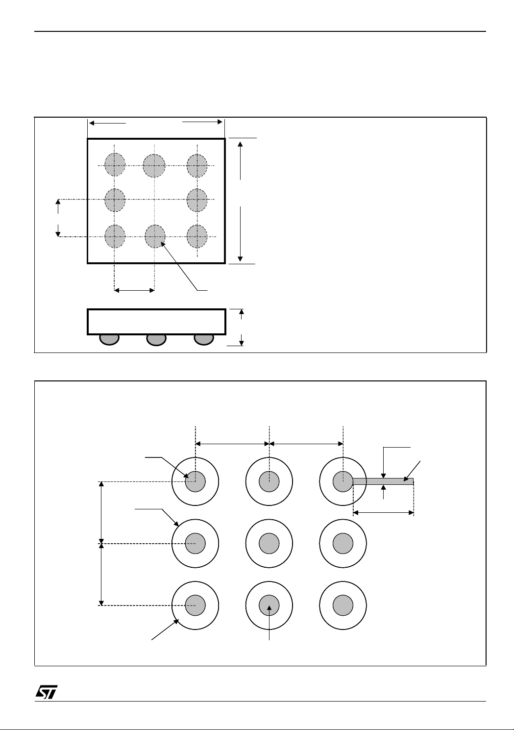
Package Mechanical Data TS922
5 Package Mechanical Data
5.1 Flip-chip package (8 bumps) - TS922IJ
Figure 14: Top view and dimensions of 8-bump flip-chip
1600 µm
1600 µm
■ Die size: 1600µm x 1600µm ±30µm
■ Die height: 350µm ±20µm
■ Die height (including bumps): 600µm
1600 µm
500µm
500µm
500µm
500µm
1600 µm
∅ 315µm
∅ 315µm
■ Bumps diameter: 315µm ±50µm
■ Bumps height: 250µm ±40µm
■ Pitch: 500µm ±10µm
600 µm
600 µm
Figure 15: Flip-chip Footprint recommendation
TS922IJ Footprint
TS922IJ Footprint
500µm
500µm
500µm
Φ=250µm
Φ=250µm
Φ=250µm
Φ=400µm
Φ=400µm
Φ=400µm
500µm
500µm
500µm
500µm
500µm
500µm
500µm
500µm
500µm
75µm min.
75µm min.
75µm min.
100µm max.
100µm max.
100µm max.
150µm min.
150µm min.
150µm min.
Track
Track
Track
Solder mask opening
Solder mask opening
Solder mask opening
Pad in Cu 1 8µm with Flash NiAu (6µm, 0.15µm)
Pad in Cu 1 8µm with Flash NiAu (6µm, 0.15µm)
Pad in Cu 1 8µm with Flash NiAu (6µm, 0.15µm)
11/16

TS922 Package Mechanical Data
Figure 16: Flip-chip marking (top view)
BUMP 1A CORNER
BUMP 1A CORNER
LEADFREE
E
E
922
922
YWW
YWW
■ Logo: ST
■ Part Number: 922
■ Date Code: YWW
■ The dot is for marking the bump
LEADFREE
Table 6: Tape & Reel specification (top view)
1
1
A
A
User direction of feed
User direction of feed
1
1
A
A
Note: Device Orientation: The devices are oriented in the carrier pocket with bump number A1 adjacent
to the sprocket holes.
12/16
Package Mechanical Data TS922
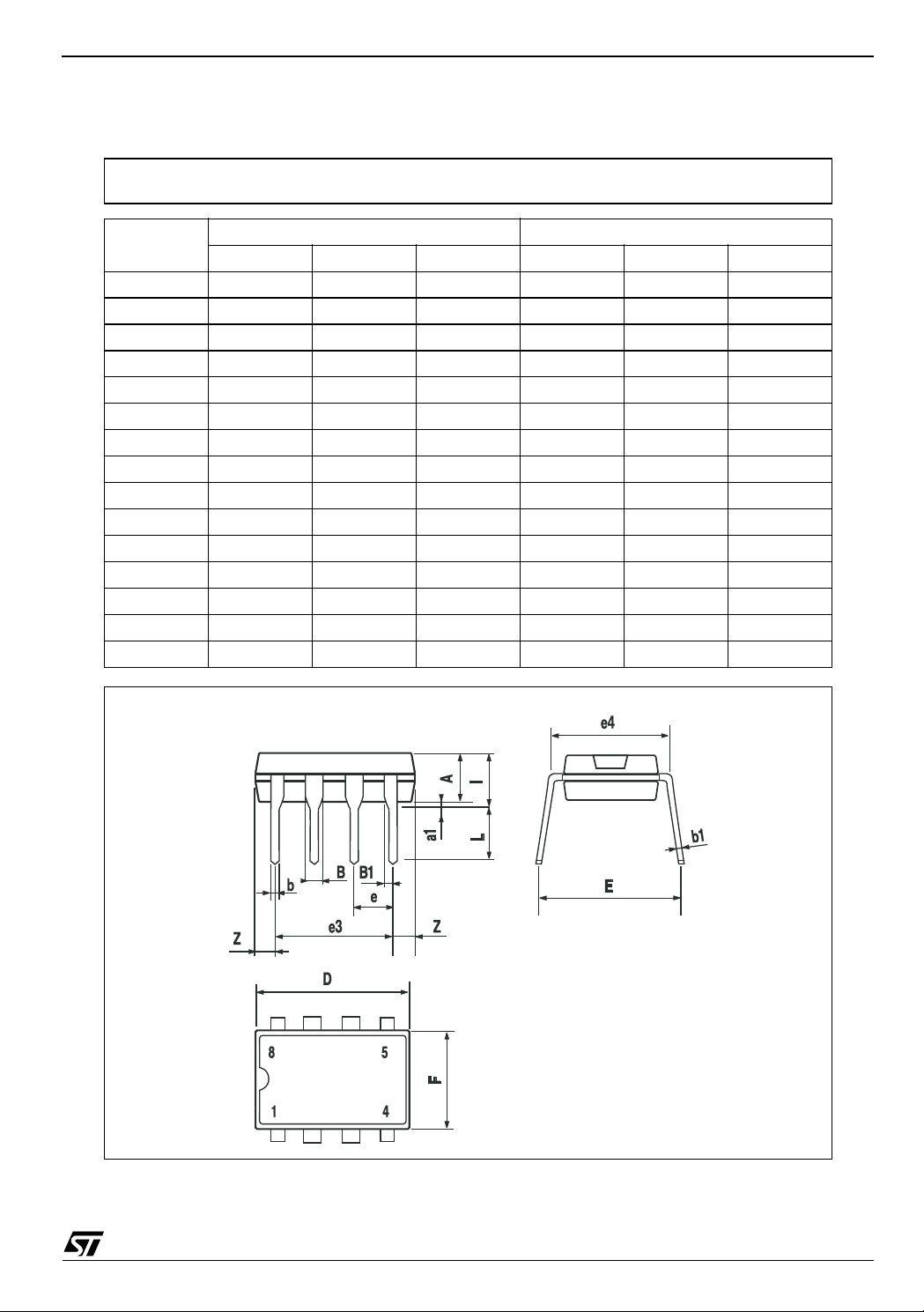
5.2 DIP8 package
Plastic DIP-8 MECHANICAL DATA
DIM.
A 3.3 0.130
a1 0.7 0.028
B 1.39 1.65 0.055 0.065
B1 0.91 1.04 0.036 0.041
b 0.5 0.020
b1 0.38 0.5 0.015 0.020
D 9.8 0.386
E 8.8 0.346
e 2.54 0.100
e3 7.62 0.300
e4 7.62 0.300
F 7.1 0.280
I 4.8 0.189
L 3.3 0.130
Z 0.44 1.6 0.017 0.063
MIN. TYP MAX. MIN. TYP. MAX.
mm. inch
P001F
13/16

TS922 Package Mechanical Data
5.3 SO8 package
SO-8 MECHANICAL DATA
DIM.
A 1.35 1.75 0.053 0.069
A1 0.10 0.25 0.04 0.010
A2 1.10 1.65 0.043 0.065
B 0.33 0.51 0.013 0.020
C 0.19 0.25 0.007 0.010
D 4.80 5.00 0.189 0.197
E 3.80 4.00 0.150 0.157
e 1.27 0.050
H 5.80 6.20 0.228 0.244
h 0.25 0.50 0.010 0.020
L 0.40 1.27 0.016 0.050
k ˚ (max.)
ddd 0.1 0.04
MIN. TYP MAX. MIN. TYP. MAX.
mm. inch
8
14/16
0016023/C

Package Mechanical Data TS922
5.4 TSSOP8 package
TSSOP8 MECHANICAL DATA
DIM.
MIN. TYP MAX. MIN. TYP. MAX.
A 1.2 0.047
A1 0.05 0.15 0.002 0.006
A2 0.80 1.00 1.05 0.031 0.039 0.041
b 0.19 0.30 0.007 0.012
c 0.09 0.20 0.004 0.008
D 2.90 3.00 3.10 0.114 0.118 0.122
E 6.20 6.40 6.60 0.244 0.252 0.260
E1 4.30 4.40 4.50 0.169 0.173 0.177
e 0.65 0.0256
K0˚ 8˚0˚ 8˚
L 0.45 0.60 0.75 0.018 0.024 0.030
L1 1 0.039
mm. inch
0079397/D
15/16

Revision History TS922
6 Revision History
Date Revision Description of Changes
Feb.2001 1 First Release
July 2004 2 Flip-Chip package inserted in the document
May 2005 3
Modifications on AMR Table 1 on page 3 (explanation of Vid and Vi limits,
ESD MM and CDM values added, Rthja added)
Information furnished is believed to be accurate and reliable. However, STMicroelectronics assumes no responsibility for the consequences
of use of such information nor for any infringement of patents or other rights of third parties which may result from its use. No license is granted
by implication or otherwise under any patent or patent rights of STMicroelectronics. Specifications mentioned in this publication are subject
to change without notice. This publication supersedes and replaces all information previously supplied. STMicroelectronics products are not
authorized for use as critical components in life support devices or systems without express written approval of STMicroelectronics.
The ST logo is a registered trademark of STMicroelectronics
All other names are the property of their respective owners
© 2005 STMicroelectronics - All rights reserved
Australia - Belgium - Brazil - Canada - China - Czech Republic - Finland - France - Germany - Hong Kong - India - Israel - Italy - Japan -
Malaysia - Malta - Morocco - Singapore - Spain - Sweden - Switzerland - United Kingdom - United States of America
STMicroelectronics group of companies
www.st.com
16/16
 Loading...