

Rail-to-rail CMOS dual operational amplifier
Features
■ Rail-to-rail input and output voltage ranges
■ Single (or dual) supply operation from 2.7 to
16 V
■ Extremely low input bias current: 1 pA typ.
■ Low input offset voltage: 2 mV max.
■ Specified for 600 Ω and 100 Ω loads
■ Low supply current: 200 μA/amplifier
(V
= 3 V)
CC
■ Latch-up immunity
■ ESD tolerance: 3 kV
■ Spice macromodel included in this specification
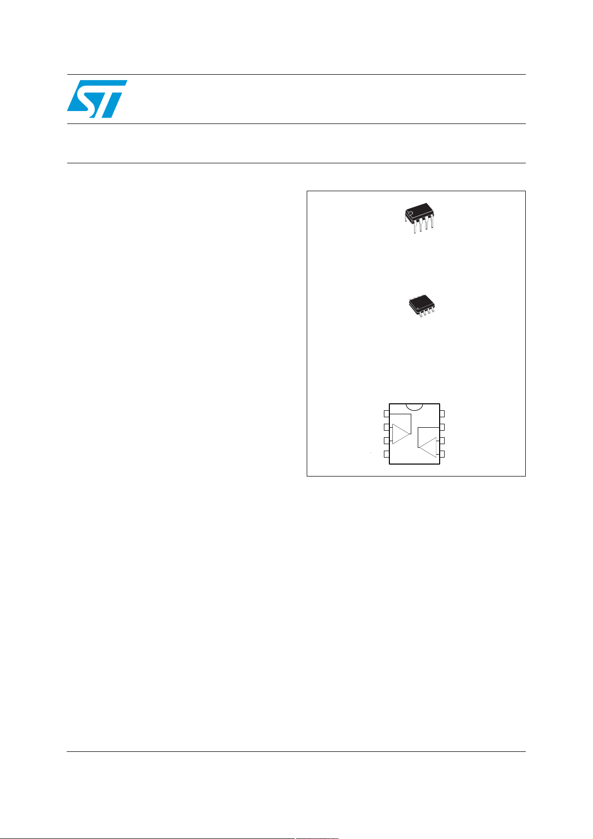
TS912, TS912A, TS912B
N
DIP-8
(Plastic package)
D
SO-8
(Plastic micropackage)
Description
The TS912 is a rail-to-rail CMOS dual operational
amplifier designed to operate with a single or dual
supply voltage.
The input voltage range V
supply rails V
The output reaches V
with R
= 10 kΩ and V
L
400 mV, with R
+
and V
CC
= 600 Ω.
L
CC
This product offers a broad supply voltage
operating range from 2.7 to 16 V and a supply
current of only 200 μA/amp (V
Source and sink output current capability is
typically 40 mA (at V
CC
limitation circuit.
includes the two
icm
-
.
CC
-
+30 mV, V
-
+300 mV, V
CC
CC
CC
CC
= 3 V).
+
-40 mV,
+
-
= 3 V), fixed by an internal
Output 1
Inverting Input 1
Non-inverting Input 1
Pin connections (top view)
+
1
2
-
+
3
V
45
CC
V
8
7
-
6
+
CC
Output 2
Inverting Input 2
Non-inverting Input 2
February 2010 Doc ID 2325 Rev 6 1/20
www.st.com
20
Absolute maximum ratings and operating conditions TS912, TS912A, TS912B
1 Absolute maximum ratings and operating conditions
Table 1. Absolute maximum ratings
Symbol Parameter Value Unit
(3)
(1)
(6)
(2)
(5)
(7)
(4)
(4)
CC
+
+0.3 V.
18 V
±18 V
-0.3 to 18 V
85
°C/W
125
41
°C/W
40
3kV
200 V
1500 V
V
CC
V
id
V
i
I
in
I
o
T
stg
T
j
Supply voltage
Differential input voltage
Input voltage
Current on inputs ±50 mA
Current on outputs ±130 mA
Storage temperature -65 to +150 °C
Maximum junction temperature 150 °C
Thermal resistance junction to ambient
R
thja
DIP8
SO-8
Thermal resistance junction to case
R
thjc
DIP8
SO-8
HBM: human body model
ESD
MM: machine model
CDM: charged device model
1. All voltage values, except differential voltage are with respect to network ground terminal.
2. Differential voltages are non-inverting input terminal with respect to the inverting input terminal.
3. The magnitude of input and output voltages must never exceed V
4. Short-circuits can cause excessive heating. Destructive dissipation can result from simultaneous short-circuits on all
amplifiers. These values are typical.
5. Human body model: a 100 pF capacitor is charged to the specified voltage, then discharged through a 1.5 kΩ resistor
between two pins of the device. This is done for all couples of connected pin combinations while the other pins are floating.
6. Machine model: a 200 pF capacitor is charged to the specified voltage, then discharged directly between two pins of the
device with no external series resistor (internal resistor < 5 Ω). This is done for all couples of connected pin combinations
while the other pins are floating.
7. Charged device model: all pins and the package are charged together to the specified voltage and then discharged directly
to the ground through only one pin. This is done for all pins.
Table 2. Operating conditions
Symbol Parameter Value Unit
V
V
T
CC
icm
oper
Supply voltage 2.7 to 16 V
Common mode input voltage range V
-0.2 to V
CC-
+0.2 V
CC+
Operating free air temperature range -40 to + 125 °C
2/20 Doc ID 2325 Rev 6

TS912, TS912A, TS912B Schematic diagram
2 Schematic diagram
Figure 1. Schematic diagram (1/2 TS912)
V
CC
Internal
Non-inverting
Input
Inverting
Input
Vref
Output
V
CC
Doc ID 2325 Rev 6 3/20

Electrical characteristics TS912, TS912A, TS912B
3 Electrical characteristics
Table 3. V
CC+
= 3 V, V
= 0 V, RL, CL connected to VCC/2, T
CC-
= 25°C (unless otherwise
amb
specified)
Symbol Parameter Min. Typ. Max. Unit
Input offset voltage (Vic = Vo = VCC/2)
TS912
TS912A
V
io
TS912B
T
min
≤ T
amb
≤ T
max
TS912
TS912A
TS912B
ΔV
I
CMR
Input offset voltage drift 5 μV/°C
io
Input offset current
I
io
T
≤ T
≤ T
≤ T
amb
amb
amb
≤ T
≤ T
≤ T
min
Input bias current
I
ib
T
min
Supply current (per amplifier, A
CC
T
min
(1)
max
(1)
max
max
Common mode rejection ratio
V
= 0 to 3 V, Vo = 1.5 V
ic
SVR Supply voltage rejection ratio (V
A
Large signal voltage gain (RL = 10 kΩ, Vo = 1.2 V to 1.8 V)
vd
T
≤ T
amb
≤ T
max
min
High level output voltage (Vid = 1 V)
= 100 kΩ
R
L
RL = 10 kΩ
= 600 Ω
R
T
min
L
R
= 100 Ω
L
≤ T
amb
≤ T
max
V
OH
RL = 10 kΩ
= 600 Ω
R
L
Low level output voltage (Vid = -1 V)
= 100 kΩ
R
L
RL = 10 kΩ
V
OL
RL = 600 Ω
= 100 Ω
R
L
T
≤ T
min
amb
≤ T
max
RL = 10 kΩ
RL = 600 Ω
1100
1150
= 1, no load)
VCL
200 300
70 dB
+
= 2.7 to 3.3 V, Vo = VCC/2) 50 80 dB
CC
3
10
2
2.95
2.9
2.3
2.96
2.6
2
2.8
2.1
30
300
900
10
5
2
12
7
3
200
300
400
V/mV
50
70
400
100
600
mV
pA
pA
μA
V
mV
Output short-circuit current (Vid = ±1 V)
I
o
GBP
Source (Vo = V
Sink (V
= V
o
CC+
CC-
)
)
Gain bandwidth product
= 100, RL = 10 kΩ, CL = 100 pF, f = 100 kHz)
(A
VCL
4/20 Doc ID 2325 Rev 6
20
20
40
mA
40
0.8 MHz

TS912, TS912A, TS912B Electrical characteristics
Table 3. V
CC+
= 3 V, V
= 0 V, RL, CL connected to VCC/2, T
CC-
= 25°C (unless otherwise
amb
specified) (continued)
Symbol Parameter Min. Typ. Max. Unit
+
SR
SR
φm Phase margin 30 Degrees
1. Maximum values include unavoidable inaccuracies of the industrial tests.
Slew rate (A
-
Slew rate (A
= 1, RL = 10 kΩ, CL = 100 pF, Vi = 1.3 V to 1.7 V) 0.4 V/μs
VCL
= 1, RL = 10 kΩ, CL = 100 pF, Vi = 1.3 V to 1.7 V) 0.3 V/μs
VCL
en Equivalent input noise voltage (R
= 100 Ω, f = 1 kHz) 30 nV/√Hz
s
Doc ID 2325 Rev 6 5/20

Electrical characteristics TS912, TS912A, TS912B
Table 4. V
CC+
= 5 V, V
= 0 V, RL, CL connected to VCC/2, T
CC-
= 25°C (unless otherwise
amb
specified)
Symbol Parameter Min. Typ. Max. Unit
Input offset voltage (Vic = Vo = VCC/2)
TS912
TS912A
V
io
TS912B
T
min
≤ T
amb
≤ T
max
TS912
TS912A
TS912B
ΔV
I
I
I
CC
CMR
Input offset voltage drift 5 μV/°C
io
Input offset current
io
T
min
Input bias current
ib
T
min
≤ T
≤ T
amb
amb
≤ T
≤ T
(1)
max
(1)
max
Supply current (per amplifier, A
≤ T
T
min
amb
≤ T
max
Common mode rejection ratio
= 1.5 to 3.5 V, Vo = 2.5 V
V
ic
SVR Supply voltage rejection ratio (V
A
Large signal voltage gain (RL = 10 kΩ, Vo = 1.5 V to 3.5 V)
vd
T
≤ T
amb
≤ T
max
min
High level output voltage (Vid = 1V)
RL = 100 kΩ
= 10 kΩ
R
L
V
OH
RL = 600 Ω
RL = 100 Ω
≤ T
T
min
amb
≤ T
max
RL = 10 kΩ
R
= 600 Ω
L
Low level output voltage (Vid = -1 V)
= 100 kΩ
R
L
= 10 kΩ
R
L
= 600 Ω
R
V
OL
L
RL = 100 Ω
≤ T
T
min
amb
≤ T
max
RL = 10 kΩ
= 600 Ω
R
L
Output short-circuit current (Vid = ±1 V)
I
o
GBP
SR
SR
Source (V
Sink (Vo = V
Gain bandwidth product
(A
VCL
+
Slew rate (A
-
Slew rate (A
= V
CC+
CC-
)
)
o
= 100, RL = 10 kΩ, CL = 100 pF, f = 100 kHz)
= 1, RL = 10 kΩ, CL = 100 pF, Vi = 1 V to 4 V) 0.8 V/μs
VCL
= 1, RL = 10 kΩ, CL = 100 pF, Vi = 1 V to 4 V) 0.6 V/μs
VCL
1 100
1 150
= 1, no load)
VCL
230 350
60 85 dB
= 3 to 5 V, Vo = VCC/2) 55 80 dB
CC+
10
40
7
4.95
4.9
4.95
4.25
4.55
3.7
4.8
4.1
40
350
1400
45
45
65
65
1MHz
10
5
2
12
7
3
200
300
450
50
100
500
150
750
mV
pA
pA
μA
V/mV
V
mV
mA
6/20 Doc ID 2325 Rev 6
 Loading...