

ST TS861, TS862, TS864 User Manual
Features
TS861, TS862, TS864
Rail-to-rail micropower BiCMOS comparators
■ Ultra low current consumption (6 µA/comp at
V
=2.7V)
CC
■ Rail to rail CMOS inputs
■ Push pull outputs
■ Supply operation from 2.7 to 10 V
■ Low propagation delay
■ ESD protection (2 kV)
■ Latch-up immunity (class A)
■ Available in SOT23-5 micropackage
Applications
■ Battery-powered systems such as alarms
■ Portable communication systems
■ Smoke/gas/fire detectors
■ Portable computers
Description
The TS86x (single, dual and quad) is a rail-to-rail
comparator characterized for 2.7 to 10 V
operation over -40° C to +85° C temperature
ranges. It exhibits an excellent speed-to-power
ratio, featuring a current consumption of 6 μA per
comparator and a response time of 500 ns at
2.7 V for a 100 mV overdrive.
Due to its ultra-low power consumption and its
availability in a tiny package, the TS86x
comparator family is perfectly suited to batterypowered systems. The output stage is designed
with a push-pull structure allowing a direct
connection to the microcontroller without
additional pull-up resistors.
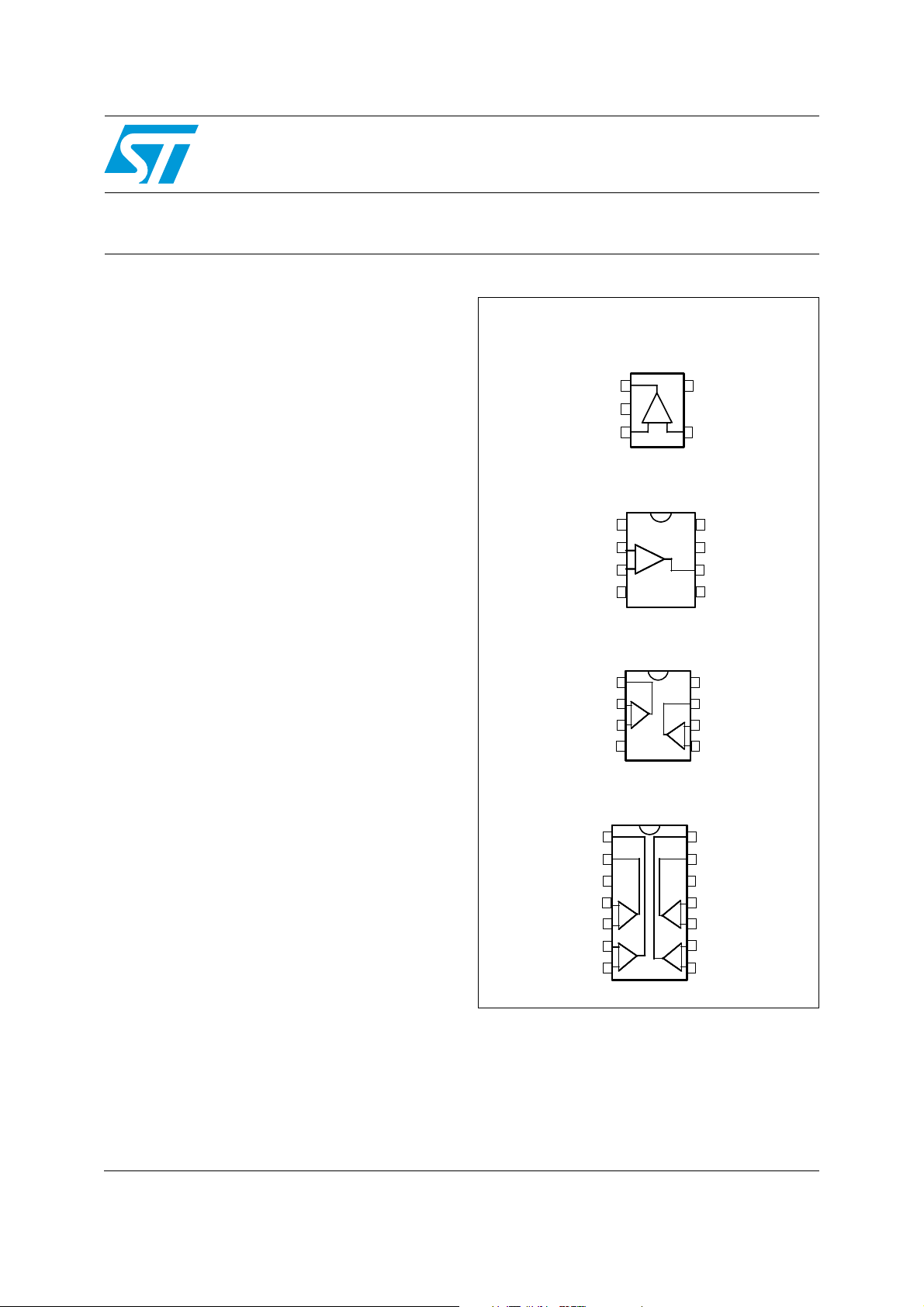
Output
Non-inverting input
Inverting input
Inverting input
Non-inverting input
Non-inverting input
Output 1
Output 1
Inverting input 1
Inverting input 1
Non-inverting input 1
Non-inverting input 1
SO-14, TSSOP14 (quad)
Output 2
Output 2
Output 1
Output 1
Vcc+
Vcc+
Inverting input 1
Inverting input 1
Non-inverting input 1
Non-inverting input 1
Inverting input 2
Inverting input 2
Non-inverting input 2
Non-inverting input 2
SOT23-5
5
4
Vcc-
1
2
+-
3
SO-8 (single)
1
NC 8
1
NC
-
-
2
2
+
+-+
3
3
Vcc-
Vcc-
4
4
8
7
7
6
6
5
5
SO-8, TSSOP8 (dual)
8
8
7
7
6
6
-
-
+
+-+
5
5
14
14
13
13
12
12
11
11
+
+-+
-
-
10
10
9
9
+
+-+
-
8
8
Vcc-
Vcc-
1
1
-
-
2
2
+
+-+
3
3
4
4
1
1
2
2
3
3
-
-
4
4
+
+-+
5
5
-
-
6
6
+
+-+
7
7
Vcc+
Inverting input
NC
NC
Vcc+
Vcc+
Output
Output
NC
NC
Vcc+
Vcc+
Output 2
Output 2
Inverting input 2
Inverting input 2
Non-inverting input 2
Non-inverting input 2
Output 3
Output 3
Output 4
Output 4
Vcc-
Vcc-
Non-inverting input 4
Non-inverting input 4
Inverting input 4
Inverting input 4
Non-inverting input 3
Non-inverting input 3
Inverting input 3
Inverting input 3
April 2009 Doc ID 6422 Rev 2 1/19
www.st.com
19
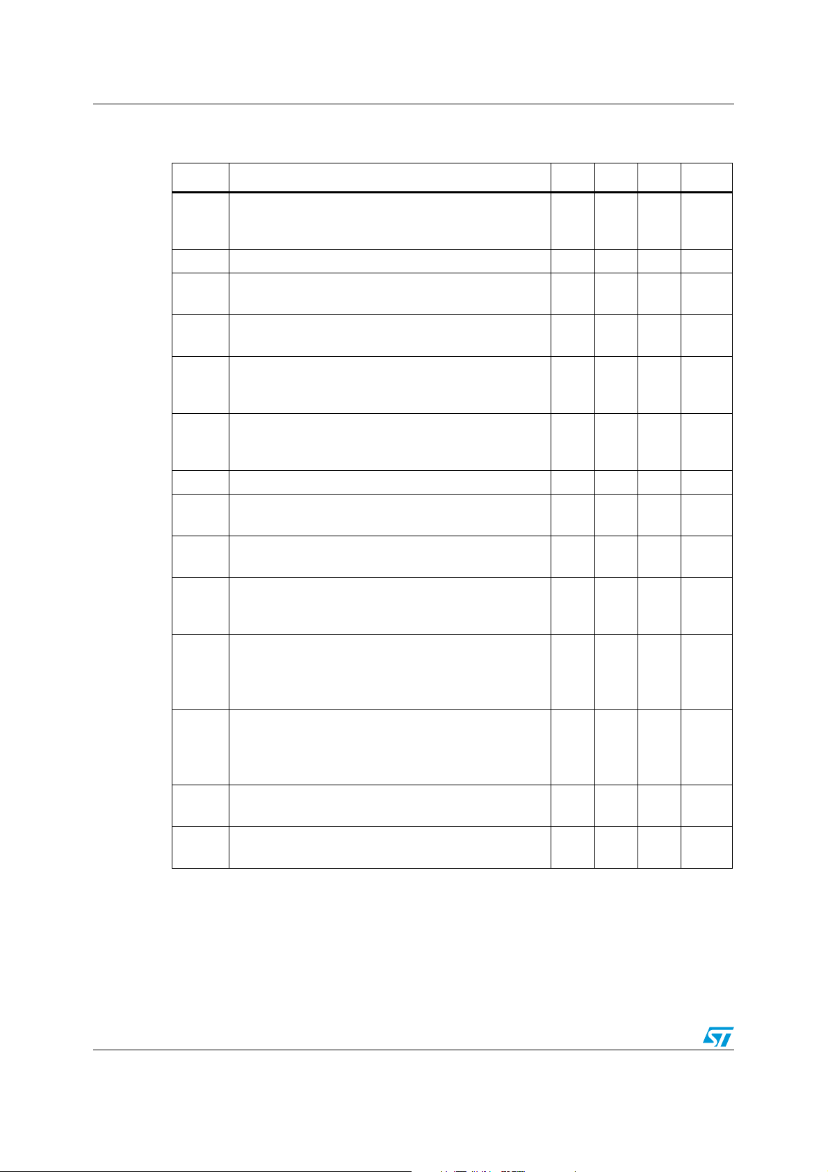
Absolute maximum ratings and operating conditions TS861, TS862, TS864
1 Absolute maximum ratings and operating conditions
Table 1. Absolute maximum ratings
Symbol Parameter Value Unit
V
V
V
Supply voltage
CC
Differential Input Voltage
ID
Input Voltage Range
IN
Thermal resistance junction to ambient
SOT23-5
R
THJA
SO8
SO14
TSSOP8
TSSOP14
Thermal resistance junction to case
SOT23-5
R
THJC
SO8
SO14
TSSOP8
TSSOP14
T
T
LEAD
ESD
Storage temperature range -65 to +150 °C
STG
T
Maximum junction temperature 150 °C
J
Lead temperature (soldering, 10 sec) 260 °C
Human body model (HBM)
Machine model (MM)
Latch-up immunity Class A
1. All voltages values, except differential voltage are with respect to network terminal.
2. Differential voltages are non-inverting input terminal with respect to the inverting input terminal.
3. The magnitude of input and output voltages must never exceed VCC +0.3V.
4. Short-circuits can cause excessive heating. These values are typical.
5. Human body model: a 100 pF capacitor is charged to the specified voltage, then discharged through a
1.5 kΩ resistor between two pins of the device. This is done for all couples of connected pin combinations
while the other pins are floating.
6. Machine model: a 200 pF capacitor is charged to the specified voltage, then discharged directly between
two pins of the device with no external series resistor (internal resistor < 5 Ω). This is done for all couples of
connected pin combinations while the other pins are floating.
(1)
(3)
(6)
(2)
(5)
(4)
(4)
12 V
±12 V
-0.3 to 12.3 V
250
125
105
°C/W
120
100
81
40
31
°C/W
37
32
2
kV
200
V
Table 2. Operating conditions
Symbol Parameter Value Unit
V
V
T
Supply voltage 2.7 to 10 V
CC
Common mode input voltage range V
ICM
Operating free air temperature range -40 to + 85 °C
Oper
2/19 Doc ID 6422 Rev 2
CC
-
- 0.3 to V
+
+ 0.3 V
CC
TS861, TS862, TS864 Electrical characteristics
2 Electrical characteristics
Table 3. Electrical characteristics at VCC = 2.7 V, T
(unless otherwise specified)
Symbol Parameter Min. Typ. Max. Unit
Input offset voltage
TS861/2/4
V
IO
ΔV
IO
I
IO
I
IB
V
OH
V
OL
A
VD
CMR
SVR
I
CC
T
PLH
T
PHL
Tmin<T<Tmax
TS861/2/4A
Tmin<T<Tmax
Input offset voltage drift 6 μV/°C
Input offset current
(1)
Tmin<T<Tmax
Input bias current
(1)
Tmin<T<Tmax
High level output voltage
I
SOURCE
=2.5mA
Tmin<T<Tmax
Low level output voltage
=2.5mA
I
SINK
Tmin<T<Tmax
Large signal voltage gain
(2)
Common mode rejection ratio
0 < V
< 2.7 V 65
ICM
Supply voltage rejection ratio
0 < V
CC
< 10V
Supply current per comparator
no load, output low
no load, output high
Propagation delay from output low to output high
= 1.35 V, f = 10 kHz, CL=50pF
V
ICM
overdrive = 10 mV
overdrive = 100 mV
Propagation delay from output high to output low
= 1.35 V, f = 10 kHz, CL=50pF
V
ICM
overdrive = 10 mV
overdrive = 100 mV
amb
= 25° C
2.35
2.15
3
15
18
3
7
mV
10
1150
300
1300
600
pA
pA
2.45
0.2 0.35
0.45
240 dB
dB
80
6
12
8
14
dB
μA
1.5
0.6
1.5
0.5
V
V
µs
µs
Doc ID 6422 Rev 2 3/19

Electrical characteristics TS861, TS862, TS864
Table 3. Electrical characteristics at VCC = 2.7 V, T
amb
= 25° C
(unless otherwise specified) (continued)
Symbol Parameter Min. Typ. Max. Unit
Fall time
T
F
f = 10 kHz, C
Rise time
T
R
f = 10 kHz, C
1. Maximum values including unavoidable inaccuracies of the industrial tests.
2. Design evaluation.
= 50 pF, overdrive = 100 mV 20 ns
L
= 50 pF, overdrive = 100 mV
L
20 ns
Note: Limits are 100% production tested at 25° C. Limits over temperature are guaranteed through
correlation and by design.
4/19 Doc ID 6422 Rev 2
TS861, TS862, TS864 Electrical characteristics
Table 4. Electrical characteristics at V
CC
= 5 V, T
amb
= 25° C
(unless otherwise specified)
Symbol Parameter Min. Typ. Max. Unit
Input offset voltage
V
IO
ΔV
I
IO
I
IB
V
OH
V
OL
A
VD
CMR
SVR
I
CC
TS861/2/4
Tmin<T<Tmax
TS861/2/4A
Tmin<T<Tmax
Input offset voltage drift 6 μV/°C
IO
Input offset current
(1)
Tmin<T<Tmax
Input bias current
(1)
Tmin<T<Tmax
High level output voltage
I
SOURCE
=5mA
Tmin<T<Tmax
4.6
4.45
Low level output voltage
I
=5mA
SINK
Tmin<T<Tmax
Large signal voltage gain
(2)
Common mode rejection ratio
0 < V
< 5 V 70
ICM
Supply voltage rejection ratio
2.7 < V
< 10 V 80
CC
Supply current per comparator
no load, output low
no load, output high
3
15
18
3
mV
7
10
1150
300
1300
600
pA
pA
4.8
0.2 0.4
0.55
240 dB
dB
dB
6
12
8
14
μA
V
V
Propagation delay from output low to output high
= 2.5 V, f = 10 kHz, CL=50pF
V
T
T
PLH
PHL
T
ICM
overdrive = 10 mV
overdrive = 100 mV
Propagation delay from output high to output low
V
= 2.5 V, f = 10 kHz, CL=50pF
ICM
overdrive = 10 mV
overdrive = 100 mV
Fall time
F
2
0.5
2
0.4
f = 10 kHz, CL= 50 pF, overdrive = 100 mV 20 ns
Rise time
T
R
f = 10 kHz, CL= 50 pF, overdrive = 100 mV 20 ns
1. Maximum values including unavoidable inaccuracies of the industrial test.
2. Design evaluation.
Note: Limits are 100% production tested at 25°C. Limits over temperature are guaranteed through
correlation and by design.
Doc ID 6422 Rev 2 5/19
µs
µs
Electrical characteristics TS861, TS862, TS864
Table 5. Electrical characteristics at V
= +10 V, T
CC
amb
= 25° C
(unless otherwise specified)
Symbol Parameter Min. Typ. Max. Unit
V
ΔV
Input offset voltage (V
IO
TS861/2/4
Tmin<T<Tmax
Input offset voltage drift 6 μV/°C
IO
Input offset current
I
IO
I
IB
Tmin<T<Tmax
Input bias current
Tmin<T<Tmax
(1)
(1)
= VCC / 2)
ICM
315
18
1150
300
1300
600
High level output voltage
V
OH
I
SOURCE
Tmin<T<Tmax
=5mA
9.6
9.45
9.8
Low level output voltage
V
OL
A
VD
CMR
SVR
=5mA
I
SINK
Tmin<T<Tmax
Large signal voltage gain
(2)
Common mode rejection ratio
0 < V
< 10 V 75
ICM
Supply voltage rejection ratio
2.7 < V
< 10V 80
CC
0.2 0.4
0.55
240 dB
Supply current per comparator
I
CC
no load, output low
no load, output high
10
7
14
16
Propagation delay from output low to output high
= 5 V, f = 10 kHz, CL=50pF
V
T
PLH
ICM
overdrive = 10 mV
overdrive = 100 mV
3
0.5
Propagation delay from output high to output low
= 5 V, f = 10 kHz, CL=50pF
V
F
ICM
overdrive = 10 mV
overdrive = 100 mV
Fall time
f = 10 kHz, C
L
Rise time
f = 10 kHz, C
L
2.6
0.4
= 50 pF, overdrive = 100 mV 20 ns
= 50 pF, overdrive = 100 mV 20 ns
T
PHL
T
T
R
1. Maximum values including unavoidable inaccuracies of the industrial test.
2. Design evaluation.
Note: Limits are 100% production tested at 25° C. Limits over temperature are guaranteed through
correlation and by design.
mV
pA
pA
V
V
dB
dB
μA
µs
µs
6/19 Doc ID 6422 Rev 2
 Loading...