

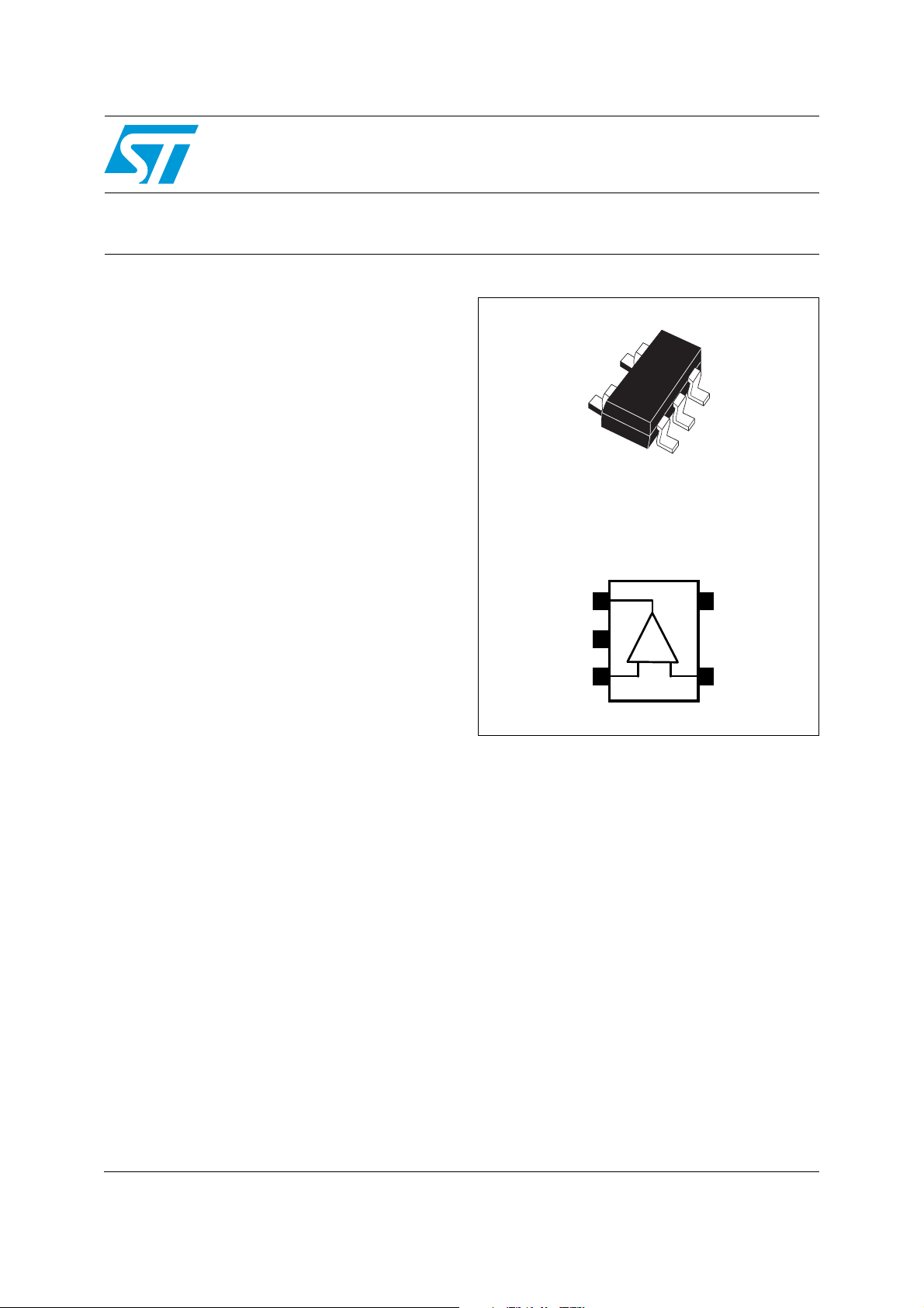
Single BiCMOS rail-to-rail micropower comparator
Features
■ Rail-to-rail inputs
■ Open drain output
■ Supply operation from 2.7 to 10 V
■ Typical supply current: 6 µA at 5 V
■ Response time of 0.5 µs at 5 V
■ Low input current
■ ESD protection: 2 kV (HBM), 200 V (MM)
■ Available in tiny SOT23-5 package
TS7221
L
SOT23-5L
Applications
■ Battery-powered systems
■ Notebooks and PDAs
■ PCMCIA cards
■ Cellular and mobile communications
■ Alarms and security systems
■ Replacement of amplifiers used in comparator
configurations for improved performance.
Description
The TS7221 is a micropower comparator
featuring a rail-to-rail input performance in a tiny
SOT23-5 package. This comparator is ideally
suited to space and weight-critical applications. It
is fully specified at 2.7-, 5- and 10-V operation
over industrial temperature ranges
(-40°C to +85°C).
The TS7221 features an open-drain output stage.
The speed-to-power ratio makes this device ultraversatile for a wide range of applications.
TS7221 open drain output
OUT
Vcc+
IN+
1
2
+
3
5
-
4
Vcc-
IN-
March 2009 Rev 5 1/13
www.st.com
13
Absolute maximum ratings TS7221
1 Absolute maximum ratings
Table 1. Absolute maximum ratings
Symbol Parameter Value Unit
V
CC
V
ID
V
IN
V
OUT
I
IN
I
OUT
R
thja
R
thjc
T
Lead
T
stg
T
J
ESD
1. The magnitude of input voltages must never exceed 0.3 V beyond the supply voltage.
2. Short-circuits can cause excessive heating. These values are typical.
3. Human body model: a 100 pF capacitor is charged to the specified voltage, then discharged through a
1.5 kΩ resistor between two pins of the device. This is done for all couples of connected pin combinations
while the other pins are floating.
4. Machine model: a 200 pF capacitor is charged to the specified voltage, then discharged directly between
two pins of the device with no external series resistor (internal resistor < 5 Ω). This is done for all couples of
connected pin combinations while the other pins are floating.
Table 2. Operating conditions
Supply voltage 12 V
Differential input voltage (V
Input voltage
(1)
(V
-
) -0.3 to (V
CC
-
) -0.3 to (V
CC
+
) +0.3 V
CC
+
) +0.3 V
CC
Output voltage 12 V
Current at input pins
(1)
± 5 mA
Current at output pin ± 30 mA
(2)
(2)
250
°C/W
°C/W
Thermal resistance junction to ambient
SOT23-5
Thermal resistance junction to case
SOT23-5 81
Lead temperature (soldering 10 seconds) 260 °C
Storage temperature -65 to +150 °C
Junction temperature 150 °C
(4)
(3)
2000
200
Human body model (HBM)
Machine model (MM)
V
Symbol Parameter Value Unit
V
T
V
CC
amb
icm
Supply voltage 2.7 to 10 V
Ambient temperature -40 to +85 °C
Common mode input voltage range (V
2/13
-
) -0.3 to (V
CC
+
) +0.3 V
CC
TS7221 Electrical characteristics
2 Electrical characteristics
Table 3. Electrical characteristics at V
+
=2.7V, T
CC
= 25° C (unless otherwise specified)
amb
Symbol Parameter Min. Typ. Max. Unit
Input offset voltage (full common mode range)
– TS7221A
V
IO
at T
min
≤ T
amb
≤ T
max
– TS7221B
at T
≤ T
amb
amb
amb
≤ T
≤ T
≤ T
(2)
max
max
(2)
max
ΔV
min
Input offset voltage drift with temperature 6 µV/oC
IO
I
IB
I
IO
Input bias current
at T
≤ T
min
Input offset current
≤ T
at T
min
CMRR Common-mode rejection ratio (0 < V
PSRR Power supply rejection ratio (2.7 < V
≤ T
≤ T
amb
amb
(3)
≤ T
≤ T
max
max
sink
= 5 mA
A
VD
V
icm
I
OH
V
OL
Voltage gain
Input common mode voltage range
at T
min
High level output voltage (IN+= 0.5 V, IN-= 0 V and
OUT = 10 V)
Low level output voltage, I
at T
min
1 300
1 150
< 2.7 V) 65 dB
icm
< 10 V) 80 dB
CC
240 dB
-0.3
0.0
0.1 500 nA
0.2 0.35
7
10
15
18
600
300
3
2.7
0.45
Supply current
I
CC
Output low
Output high
6
8
12
14
(1)
mV
pA
pA
V
V
µA
Response time low to high
(V
= 1.35 V, CL=50pF, RL=10kΩ)
T
PLH
ic
Overdrive = 10 mV
Overdrive = 100 mV
1.5
0.6
Response time high to low
= 1.35 V, CL=50pF, RL=10kΩ)
(V
T
PHL
T
F
T
R
1. Limits are 100% production-tested at +25° C. Behavior at temperature range limits is guaranteed through correlation and
by design.
2. Maximum values include unavoidable inaccuracies of industrial testing.
3. Design evaluation.
ic
Overdrive = 10 mV
Overdrive = 100 mV
Fall time
= 50 pF, RL=5kΩ, overdrive = 10 mV
C
L
Rise time
CL = 50 pF, RL=5kΩ, overdrive = 10 mV
1.5
0.5
0.3 µs
0.3 µs
3/13
µs
µs
Electrical characteristics TS7221
Table 4. Electrical characteristics for V
CC
+
= 5 V, T
= 25° C (unless otherwise specified)
amb
Symbol Parameter Min. Typ. Max. Unit
Input offset voltage (full common mode range)
– TS7221A
V
IO
at T
min
≤ T
amb
≤ T
max
– TS7221B
≤ T
≤ T
≤ T
amb
amb
amb
≤ T
≤ T
≤ T
max
(2)
max
max
(2)
ΔV
T
min
Input offset voltage drift with temperature 6 µV/oC
IO
I
IB
I
IO
Input bias current
at T
min
Input offset current
at T
min
CMRR Common-mode rejection ratio (0 < V
PSRR Power supply rejection ratio (2.7 < V
≤ T
min
amb
≤ T
(3)
≤ T
amb
max
≤ T
max
sink
= 5 mA
A
VD
V
icm
I
OH
V
OL
Voltage gain
Input common mode voltage range
at T
min
High level output voltage
(IN+= 0.5 V, IN-= 0 V and OUT = 10 V) 0.1 500
Low level output voltage, I
at T
1 300
1 150
< 5 V) 70 dB
icm
< 10 V) 80 dB
CC
240 dB
-0.3
0.0
0.2 0.40
7
10
15
18
600
300
5.3
5.0
0.55
Supply current
I
CC
Output low
Output high
6
8
12
14
(1)
mV
pA
pA
V
nA
V
µA
Response time low to high
T
PLH
(Vic= 2.5 V, CL =50pF, RL=10kΩ)
Overdrive = 10 mV
Overdrive = 100 mV
2
0.5
Response time high to low
= 2.5 V, CL = 50 pF, RL=10kΩ)
(V
T
PHL
T
F
T
R
1. Limits are 100% production-tested at +25° C. Behavior at temperature range limits is guaranteed through correlation and
by design.
2. Maximum values include unavoidable inaccuracies of industrial testing.
3. Design evaluation.
ic
Overdrive = 10 mV
Overdrive = 100 mV
Fall time
= 50 pF, RL=5kΩ, overdrive = 10 mV
C
L
Rise time
CL = 50 pF, RL=5kΩ, overdrive = 10 mV
2
0.4
0.3 µs
0.3 µs
µs
µs
4/13

TS7221 Electrical characteristics
Table 5. Electrical characteristics for V
+
=10V, T
CC
= 25° C (unless otherwise specified)
amb
Symbol Parameter Min. Typ. Max. Unit
Input offset voltage (full common mode range)
– TS7221A
V
IO
at T
min
≤ T
amb
≤ T
max
– TS7221B
T
≤ T
≤ T
≤ T
amb
amb
amb
≤ T
≤ T
≤ T
max
(2)
max
max
(2)
ΔV
min
Input offset voltage drift with temperature 6 μV/oC
IO
I
IB
I
IO
Input bias current
at T
min
Input offset current
at T
min
CMRR Common-mode rejection ratio (0 < V
PSRR Power supply rejection ratio (2.7 < V
≤ T
≤ T
(3)
240 dB
≤ T
amb
max
= 5 mA
sink
≤ T
amb
max
A
VD
V
ICM
I
OH
V
OL
Voltage gain
Input common mode voltage range
at T
min
High level output voltage
+
= 0.5 V, IN-= 0 V and OUT = 10 V) 0.1 500
(IN
Low level output voltage, I
at T
min
1 300
1 150
< 10 V) 75 dB
icm
< 10 V) 80 dB
CC
-0.3
0.0
0.2 0.40
7
10
15
18
600
300
10.3
10.0
0.55
Supply current
I
CC
Output low
Output high
10
7
14
16
Response time low to high
= 5 V, CL = 50 pF, RL=10kΩ)
(V
T
PLH
ic
Overdrive = 10 mV
Overdrive = 100 mV
3
0.5
Response time high to low
= 5 V, CL = 50 pF, RL=10kΩ)
(V
T
PHL
ic
Overdrive = 10 mV
Overdrive = 100 mV
4
0.4
(1)
mV
pA
pA
V
nA
V
μA
μs
μs
T
T
1. Limits are 100% production-tested at +25° C. Behavior at temperature range limits is guaranteed through correlation and
by design.
2. Maximum values include unavoidable inaccuracies of industrial testing.
3. Design evaluation.
Fall time
F
CL = 50 pF, RL=5kΩ, overdrive = 10 mV
Rise time
R
= 50 pF, RL=5kΩ, overdrive = 10 mV
C
L
0.3 μs
0.3 μs
5/13

Electrical characteristics TS7221
Figure 1. Supply current vs. supply voltage
(output low)
10
T=+85°C
8
6
4
Supply current (µA)
2
0
0246810
T=+25°C
Supply voltage (V)
Output low
No load
T=-40°C
Figure 3. Output sinking current vs. output
voltage at V
1.0
0.8
0.6
T
AMB
0.4
Output voltage (V)
0.2
0.0
T
=+25°C
AMB
0246810
Figure 5. VIO vs. V
V
=5V
CC
4
T = -40°C
2
0
=+2.7V, VCC=+5V
CC
=+85°C
Sink current (mA)
and temperature at
icm
T = +85°C
VCC = + 5V
Output Low
T
=-40°C
AMB
T = +25°C
Figure 2. Supply current vs. supply voltage
(output high)
12
T=+85°C
10
8
6
Supply current (µA)
4
2
0
0246810
Figure 4. V
4
2
0
Input offset voltage (mV)
IO
V
-2
-4
0.0 0.5 1.0 1.5 2.0 2.5 3.0
Figure 6. V
6
4
2
0
T=+25°C
Supply voltage (V)
vs. V
IO
V
CC
IO
V
CC
icm
=2.7V
T = -40°C
V
Common mode voltage (V)
ICM
vs. V
icm
=10V
T=-40°C
Output high
and temperature at
T = +85°C
T = +25°C
and temperature at
T = +25°C
T = +85°C
Input offset voltage (mV)
IO
V
-2
-4
012345
V
Common mode voltage (V)
ICM
6/13
Input offset voltage (mV)
-2
IO
V
-4
-6
0246810
T = -40°C
V
Common mode voltage (V)
ICM

TS7221 Electrical characteristics
Figure 7. T
4
T
=+25°C
AMB
R
=10kΩ & CL=50pF
L
3
2
1
(µs) with 10mV overdrive
PLH
T
0
Figure 9. T
4
T
=+25°C
AMB
=10kΩ & CL=50pF
R
L
3
PLH
vs V
at VCC=10V and
icm
Figure 8. T
10 mV overdrive
0510
Common mode voltage (V)
PLH
vs V
at VCC= 5 V and 10 mV
icm
Figure 10. T
overdrive
PLH
vs V
at VCC= 10 V and
icm
100 mV overdrive
4
T
=+25°C
AMB
=10kΩ & CL=50pF
R
L
3
2
1
(µs) with 100mV overdrive
PLH
T
0
0510
Common mode voltage (V)
PLH
vs V
at VCC=5V and
icm
100 mV overdrive
4
T
=+25°C
AMB
=10kΩ & CL=50pF
R
L
3
2
1
(µs) with 10mV overdrive
PLH
T
0
0.0 2.5 5.0
Figure 11. T
5
4
3
2
(µs) with 10mV overdrive
1
PHL
T
0
Common mode voltage (V)
PHL
vs V
at VCC= 10 V and
icm
Figure 12. T
10 mV overdrive
T
=+25°C
AMB
=10kΩ & CL=50pF
R
L
0510
Common mode voltage (V)
2
1
(µs) with 100mV overdrive
PLH
T
0
0.0 2.5 5.0
Common mode voltage (V)
PHL
vs V
at VCC= 10 V and
icm
100 mV overdrive
5
4
3
2
1
(µs) with 100mV overdrive
PHL
T
0
0510
Common mode voltage (V)
T
=+25°C
AMB
=10kΩ & CL=50pF
R
L
7/13

Electrical characteristics TS7221
Figure 13. T
3
2
1
(µs) with 10mV overdrive
PHL
T
0
0.0 2.5 5.0
PHL
vs V
at VCC=5V and 10 mV
icm
overdrive
Common mode voltage (V)
T
=+25°C
AMB
=10kΩ & CL=50pF
R
L
Figure 14. T
3
2
1
(µs) with 100mV overdrive
PHL
T
0
0.0 2.5 5.0
PHL
vs V
at VCC=5V and
icm
100 mV overdrive
Common mode voltage (V)
T
=+25°C
AMB
=10kΩ & CL=50pF
R
L
8/13

TS7221 Package information
3 Package information
In order to meet environmental requirements, ST offers these devices in different grades of
ECOPACK
specifications, grade definitions and product status are available at: www.st.com.
ECOPACK
®
packages, depending on their level of environmental compliance. ECOPACK®
®
is an ST trademark.
9/13

Package information TS7221
3.1 SOT23-5 package information
Figure 15. SOT23-5L package mechanical drawing
Table 6. SOT23-5L package mechanical data
Dimensions
Ref.
Min. Typ. Max. Min. Typ. Max.
A 0.90 1.20 1.45 0.035 0.047 0.057
A1 0.15 0.006
A2 0.90 1.05 1.30 0.035 0.041 0.051
B 0.35 0.40 0.50 0.013 0.015 0.019
C 0.09 0.15 0.20 0.003 0.006 0.008
D 2.80 2.90 3.00 0.110 0.114 0.118
D1 1.90 0.075
e 0.95 0.037
E 2.60 2.80 3.00 0.102 0.110 0.118
F 1.50 1.60 1.75 0.059 0.063 0.069
L 0.10 0.35 0.60 0.004 0.013 0.023
K 0 degrees 10 degrees
Millimeters Inches
10/13

TS7221 Ordering information
4 Ordering information
Table 7. Order codes
Order code Temperature range Package Packing Marking
TS7221AILT
-40°C, +85°C SOT23-5L Tape & reel
TS7221BILT K519
K518
11/13

Revision history TS7221
5 Revision history
Table 8. Document revision history
Date Revision Changes
01-Dec-2002 1 Initial release
Update of datasheet presentation and format.
Change of T
to Pb-free package.
Corrections to V
01-Sep-2005 2
tables.
Addition of Pb-free information in Section 3: Package information on
page 9.
Correction to package mechanical data given in
Figure 15 on page 10.
26-Mar-2007 3
Added automotive grade part numbers in Section 4: Ordering
information on page 11.
05-Jul-2007 4 Corrected automotive grade part numbers in Table 7: Order codes.
Added notes for ESD in Table 1: Absolute maximum ratings.
Added Rthja and Rthjc parameters in Table 1: Absolute maximum
ratings.
27-Mar-2009 5
Removed power dissipation parameter (P
maximum ratings.
Updated package information in Section 3.1.
Removed automotive grade part numbers in Table 7: Order codes.
temperature in Table 1 on page 2, to reflect change
lead
upper rail parameters in Electrical characteristics
icm
) in Table 1: Absolute
D
12/13

TS7221
Please Read Carefully:
Information in this document is provided solely in connection with ST products. STMicroelectronics NV and its subsidiaries (“ST”) reserve the
right to make changes, corrections, modifications or improvements, to this document, and the products and services described herein at any
time, without notice.
All ST products are sold pursuant to ST’s terms and conditions of sale.
Purchasers are solely responsible for the choice, selection and use of the ST products and services described herein, and ST assumes no
liability whatsoever relating to the choice, selection or use of the ST products and services described herein.
No license, express or implied, by estoppel or otherwise, to any intellectual property rights is granted under this document. If any part of this
document refers to any third party products or services it shall not be deemed a license grant by ST for the use of such third party products
or services, or any intellectual property contained therein or considered as a warranty covering the use in any manner whatsoever of such
third party products or services or any intellectual property contained therein.
UNLESS OTHERWISE SET FORTH IN ST’S TERMS AND CONDITIONS OF SALE ST DISCLAIMS ANY EXPRESS OR IMPLIED
WARRANTY WITH RESPECT TO THE USE AND/OR SALE OF ST PRODUCTS INCLUDING WITHOUT LIMITATION IMPLIED
WARRANTIES OF MERCHANTABILITY, FITNESS FOR A PARTICULAR PURPOSE (AND THEIR EQUIVALENTS UNDER THE LAWS
OF ANY JURISDICTION), OR INFRINGEMENT OF ANY PATENT, COPYRIGHT OR OTHER INTELLECTUAL PROPERTY RIGHT.
UNLESS EXPRESSLY APPROVED IN WRITING BY AN AUTHORIZED ST REPRESENTATIVE, ST PRODUCTS ARE NOT
RECOMMENDED, AUTHORIZED OR WARRANTED FOR USE IN MILITARY, AIR CRAFT, SPACE, LIFE SAVING, OR LIFE SUSTAINING
APPLICATIONS, NOR IN PRODUCTS OR SYSTEMS WHERE FAILURE OR MALFUNCTION MAY RESULT IN PERSONAL INJURY,
DEATH, OR SEVERE PROPERTY OR ENVIRONMENTAL DAMAGE. ST PRODUCTS WHICH ARE NOT SPECIFIED AS "AUTOMOTIVE
GRADE" MAY ONLY BE USED IN AUTOMOTIVE APPLICATIONS AT USER’S OWN RISK.
Resale of ST products with provisions different from the statements and/or technical features set forth in this document shall immediately void
any warranty granted by ST for the ST product or service described herein and shall not create or extend in any manner whatsoever, any
liability of ST.
ST and the ST logo are trademarks or registered trademarks of ST in various countries.
Information in this document supersedes and replaces all information previously supplied.
The ST logo is a registered trademark of STMicroelectronics. All other names are the property of their respective owners.
© 2009 STMicroelectronics - All rights reserved
STMicroelectronics group of companies
Australia - Belgium - Brazil - Canada - China - Czech Republic - Finland - France - Germany - Hong Kong - India - Israel - Italy - Japan -
Malaysia - Malta - Morocco - Singapore - Spain - Sweden - Switzerland - United Kingdom - United States of America
www.st.com
13/13
 Loading...