

TS7211
SINGLE BiCMOS RAIL TO RAIL
µPOWER COMPARATOR
■ RAIL TO RAIL INPUTS
■ PUSH-PULL OUTPUT
■ SUPPLY OPERATION FROM 2.7V TO 10V
■ TYPICAL SUPPLY CURRENT: 6µA @ 5V
■ RESPONSE TIME OF 0. 5µs AT 5V
■ LOW INPUT CURRENT
■ ESD PROTECTION : 2KV (HBM) 2 00V (MM)
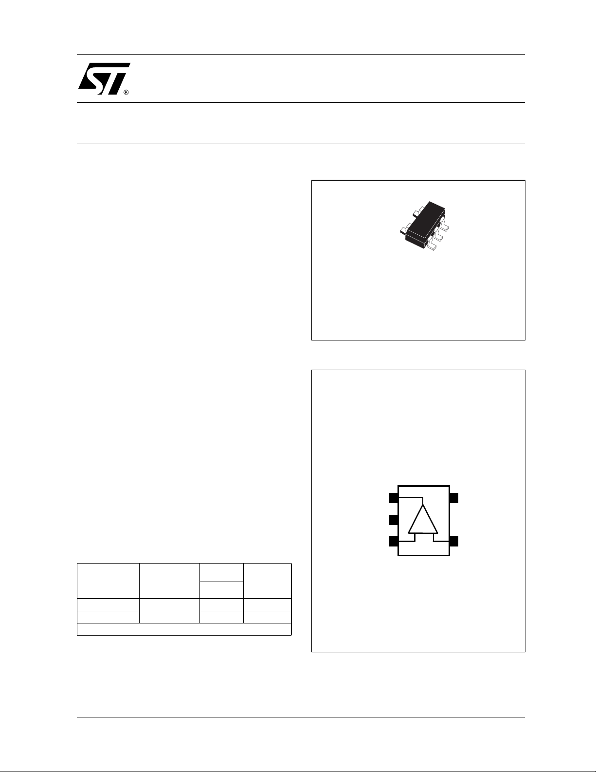
■ AVAILABLE IN TINY SOT23-5 PACKAGE
DESCRIPTION
The TS7211 is a micropower comparator
featuring rail to rail input performance in a tiny
SOT23-5 package. This comparator is ideally
suited to space and weight critical applications. It
is fully specified at 2.7V, 5V and 10V operations
over the industrial temperature range (-40/+85°C).
The TS7211 features a push-pull output stage.
The speed to power ratio mak es this device ultra
versatile for a wide range of applications.
APPLICATIONS
■ Battery powered systems
■ Notebooks and PDAs
■ PCMCIA cards
■ Cellulars and mobile communication
■ Alarm and security systems
■ Replacement of amplifiers used in
comparator configuration with better
performances
ORDER CODE
L
SOT23-5L
(Tiny Package)
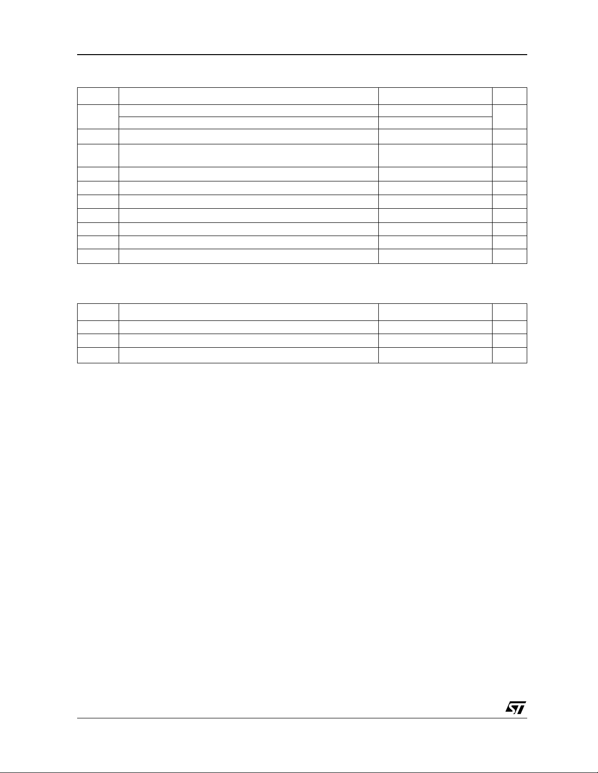
PIN CONNECTIONS (top view)
TS7211 Push-Pull output
OUT
Vcc+
IN+
1
2
+
3
5
4
Vcc-
IN-
Part Number
TS7211AI
TS7211BI
Example : TS7211AILT
L = Tiny Package (SOT23-5) - only available in Tape & Reel (LT)
May 2002
Temperature
Range
-40°C, +85°C
Package
L
•
•
SOT23-5
Marking
K515
K516
1/9
TS7211
ABSOLUTE MAXIMUM RATINGS
Symbol Parameter Value Unit
ESD
V
V
V
I
T
T
1. The magnitude of input and output voltages must never exceed 0.3V beyond the supply voltage.
2. T
Human body model (HBM) 2000
Machine model (MM) 200
V
Differential Input Voltage
ID
&
IN
Input and output Voltages
OUT
Supply voltage 12 V
CC
I
Current at input pins ± 5 mA
IN
Current at output pin ± 30 mA
OUT
Lead temperature (soldering 10 seconds) 250 °C
Lead
Storage Temperature -65 to +150 °C
STG
T
Junction Temperature 150 °C
J
P
Power dissipation 2) SOT23-5
D
= 150°C, T
J
= 25oC with R
AMB
TH-JA
1)
= 250oC/W for SOT23-5 package
(V
(V
CC
CC
-
) -0.3 to (V
-
) -0.3 to (V
CC
CC
500 mW
+
) +0.3
+
) +0.3
OPERATING CONDITIONS
Symbol Parameter Value Unit
V
T
V
Supply Voltage 2.7 to 10 V
CC
Ambient Temperature -40 to +85 °C
AMB
Common mode input voltage range
ICM
(V
CC
-
) -0.3 to (V
CC
+
) +0.3
V
V
V
V
2/9
TS7211
ELECTRICAL CHARACTERISTICS
+
V
= 2.7V, T
CC
Symbol Parameter Min. Typ. Max. Unit
V
Input Offset Voltage (Full common mode range)
IO
V
∆
CMRR
PSRR
A
V
Input Offset Voltage Drift with temperature 6
IO
I
IB
Input Bias Current
I
IO
Input Offset Current 1)
Common-mode Rejection Ratio (0 < V
Power Supply Rejection Ratio (2.7 < V
VD Voltage Gain
Input Common Mode Voltage Range (upper rail)
ICM
Input Common Mode Voltage Range (lower rail)
V
V
T
T
1) Maximum values include unavoidable inaccurates of the industrial test.
2) Design evaluation.
3) Limits are 100% production tested at +25°C. Limits over temperature are guaranteed through correlation and by design.
High Level Output Voltage - I
OH
Low Level Output Voltage - I
OL
I
Supply Current
CC
Response Time Low to High (Vic = 1.35V, CL = 50pF)
PLH
Response Time Low to High (Vic = 1.35V, CL = 50pF)
PHL
Fall Time (CL = 50pF)
T
F
T
Rise Time (CL = 50pF)
R
= 25°C (unless otherwise specified)
AMB
TS7211A
≤ T
T
MIN
AMB
≤ T
MAX
TS7211B
≤ T
≤ T
≤ T
≤ T
≤ T
≤ T
≤ T
AMB
AMB
AMB
AMB
AMB
AMB
AMB
≤ T
≤ T
≤ T
≤ T
≤ T
source
≤ T
sink
≤ T
MAX
MAX
MAX
MAX
MAX
= 2.5mA
MAX
= 2.5mA
MAX
< 2.7V)
icm
CC
< 10V)
T
MIN
1)
T
MIN
T
MIN
2)
T
MIN
T
MIN
T
MIN
T
MIN
No load, output low
No load, output high
Overdrive = 10mV
Overdrive = 100mV
Overdrive = 10mV
Overdrive = 100mV
Overdrive = 100mV
Overdrive = 100mV
3
2.7
-0.3
0.0
2.35
2.15
7
10
15
18
µ
1 300
600
1 150
300
65 dB
80 dB
240 dB
2.45 V
0.2 0.35
0.45
6
8
12
14
1.5
0.6
1.5
0.5
20 ns
20 ns
mV
V/
pA
pA
V
V
µ
µ
µ
o
C
A
s
s
3/9

TS7211
ELECTRICAL CHARACTERISTICS
+
V
= 5V, T
CC
Symbol Parameter Min. Typ. Max. Unit
V
IO
V
∆
IO
I
IB
I
IO
CMRR Common-mode Rejection Ratio (0 < V
PSRR Power Supply Rejection Ratio (2.7 < V
A
VD
V
ICM
V
OH
V
OL
I
CC
T
PLH
T
PHL
T
F
T
R
1) Maximum values include unavoidable inaccurates of the industrial test.
2) Design evaluation.
3) Limits are 100% production tested at +25°C. Limits over temperature are guaranteed through correlation and by design.
= 25°C (unless otherwise specified)
AMB
Input Offset Voltage (Full common mode range)
TS7211A
≤ T
T
MIN
AMB
≤ T
MAX
TS7211B
≤ T
T
MIN
AMB
≤ T
MAX
Input Offset Voltage Drift with temperature 6
Input Bias Current 1)
T
≤ T
AMB
≤ T
MAX
MIN
Input Offset Current 1)
≤ T
≤ T
≤ T
≤ T
≤ T
AMB
AMB
AMB
AMB
AMB
≤ T
≤ T
≤ T
source
≤ T
sink
≤ T
MAX
MAX
MAX
= 5mA
MAX
= 5mA
MAX
icm
CC
< 5V)
< 10V)
5.3
5.0
-0.3
0.0
4.6
4.45
240 dB
4.8 V
0.2 0.40
T
MIN
Voltage Gain 2)
Input Common Mode Voltage Range (upper rail)
T
MIN
Input Common Mode Voltage Range (lower rail)
T
MIN
High Level Output Voltage - I
T
MIN
Low Level Output Voltage - I
T
MIN
Supply Current
No load, output low
No load, output high
Response Time Low to High (VIC = 2.5V, CL = 50pF)
Overdrive = 10mV
Overdrive = 100mV
0.5
Response Time Low to High (Vic = 2.5V, CL = 50pF)
Overdrive = 10mV
Overdrive = 100mV
0.4
Fall Time (CL = 50pF)
Overdrive = 100mV
Rise Time (CL = 50pF)
Overdrive = 100mV
7
10
15
18
µ
1 300
600
1 150
300
70 dB
80 dB
0.55
6
8
12
14
2
2
20 ns
20 ns
mV
V/
pA
pA
V
V
µ
µ
µ
o
C
A
s
s
4/9

TS7211
ELECTRICAL CHARACTERISTICS
+
V
= 10V, T
CC
Symbol Parameter Min. Typ. Max. Unit
V
IO
V
∆
IO
I
IB
I
IO
CMRR Common-mode Rejection Ratio (0 < V
PSRR Power Supply Rejection Ratio (2.7 < V
A
VD
V
ICM
V
OH
V
OL
I
CC
T
PLH
T
PHL
T
F
T
R
1) Maximum values include unavoidable inaccurates of the industrial test.
2) Design evaluation.
3) Limits are 100% production tested at +25°C. Limits over temperature are guaranteed through correlation and by design.
= 25°C (unless otherwise specified)
AMB
Input Offset Voltage (Full common mode range)
TS7211A
≤ T
T
MIN
AMB
≤ T
MAX
TS7211B
≤ T
T
MIN
AMB
≤ T
MAX
Input Offset Voltage Drift with temperature 6
Input Bias Current 1)
≤ T
T
MIN
AMB
≤ T
MAX
Input Offset Current 1)
T
≤ T
≤ T
≤ T
≤ T
≤ T
AMB
AMB
AMB
AMB
AMB
≤ T
≤ T
≤ T
source
≤ T
sink
≤ T
MAX
MAX
MAX
= 5mA
MAX
= 5mA
MAX
< 10V)
icm
CC
< 10V)
10.3
10.0
-0.3
0.0
9.6
9.45
240 dB
9.8 V
0.2 0.40
MIN
Voltage Gain 2)
Input Common Mode Voltage Range (upper rail)
T
MIN
Input Common Mode Voltage Range (lower rail)
T
MIN
High Level Output Voltage - I
T
MIN
Low Level Output Voltage - I
T
MIN
Supply Current
No load, output low
No load, output high
Response Time Low to High (Vic = 5V, CL = 50pF)
Overdrive = 10mV
Overdrive = 100mV
0.5
Response Time Low to High (Vic = 5V, CL = 50pF)
Overdrive = 10mV
Overdrive = 100mV
0.4
Fall Time (CL = 50pF)
Overdrive = 100mV
Rise Time (CL = 50pF)
Overdrive = 100mV
7
10
15
18
µ
1 300
600
1 150
300
75 dB
80 dB
0.55
7
10
14
16
3
4
20 ns
20 ns
mV
V/
pA
pA
V
V
µ
µ
µ
o
C
A
s
s
5/9

TS7211
Supply current versus supply voltage
(Output low)
10
T=+85°C
8
6
T=-40°C
@ VCC= 5V
ICM
V
V
ICM
=0V & 5V
ICM
=2.5V
T=+25°C
4
Supply current (µA)
2
0
0246810
I
versus frequency and V
CC
VCC= 5V
120
T
= +25°C
AMB
100
A)
µ
80
60
40
Supply current (
20
0
0.1 1 10 100
Supply voltage (V)
Frequency (kHz)
versus output frequency
I
CC
and V
I
CC
@ VCC= 2.7V
ICM
VCC= 2.7V
60
T
= +25°C
AMB
A)
µ
40
Supply current (
20
0
0.1 1 10 100
V
V
ICM
ICM
= 1.35V
= 0V & 2.7V
Frequency (kHz)
versus frequency and V
200
VCC= 10V
175
T
= +25°C
AMB
150
A)
µ
125
100
75
Supply current (
50
V
= 0V
25
0
0.1 1 10 100
ICM
Frequency (kHz)
@ VCC= 10V
ICM
V
= 10V
ICM
V
= 5V
ICM
Output sink i ng current vs Output v ol tage @
Vcc = +5V
6/9
1.0
0.8
0.6
T
=+85°C
0.4
Output voltage (V)
0.2
0.0
0246810
T
AMB
=+25°C
AMB
Sink current (mA)
VCC = + 5V
Output Low
T
=-40°C
AMB
Output sourcing current vs Output voltage @
Vcc = +5V
5.0
4.8
T
=-40°C
4.6
4.4
Output voltage (V)
4.2
4.0
0246810
AMB
VCC = + 5V
Output High
T
=+25°C
AMB
T
=+85°C
AMB
Output current (mA)

T
PLH
vs V
@ VCC=10V and 10mV overdrive
ICM
T
PLH
vs V
TS7211
@ VCC=10V and 100mV overdrive
ICM
T
PLH
vs V
4
T
=+25°C
AMB
3
2
1
(µs) with 10mV overdrive
PLH
T
0
4
3
2
1
(µs) with 10mV overdrive
PLH
T
0
0510
@ VCC=5V and 10mV overdrive
ICM
T
=+25°C
AMB
0.0 2.5 5.0
Common mode voltage (V)
Common mode voltage (V)
T
PLH
(µs) with 100mV overdrive
T
vs V
(µs) with 100mV overdrive
T
4
3
2
1
PLH
0
4
3
2
1
PLH
0
0510
@ VCC=5V and 100mV overdrive
ICM
0.0 2.5 5.0
Common mode voltage (V)
T
Common mode voltage (V)
T
=+25°C
AMB
=+25°C
AMB
T
PHL
vs V
@ VCC=10V and 10mV overdrive
ICM
5
4
3
2
(µs) with 10mV overdrive
1
PHL
T
0
0510
T
=+25°C
AMB
Common mode voltage (V)
T
PHL
vs V
(µs) with 100mV overdrive
T
@ VCC=10V and 100mV overdrive
ICM
5
T
4
3
2
1
PHL
0
0510
Common mode voltage (V)
AMB
=+25°C
7/9

TS7211
T
vs V
PHL
@ VCC=5V and 10mV overdrive
ICM
T
PHL
vs V
@ VCC=5V and 100mV overdrive
ICM
V
IO
(µs) with 10mV overdrive
PHL
T
vs V
Input offset voltage (mV)
IO
V
3
T
2
1
0
0.0 2.5 5.0
Common mode voltage (V)
& Temperature @ VCC=2.7V
ICM
4
2
0
-2
T = -40°C
T = +85°C
=+25°C
AMB
T = +25°C
3
T
=+25°C
AMB
2
1
(µs) with 100mV overdrive
PHL
T
0
0.0 2.5 5.0
Common mode voltage (V)
V
IO
vs V
& Temperature @ VCC=5V
ICM
4
T = -40°C
2
0
Input offset voltage (mV)
IO
V
-2
T = +85°C T = +25°C
VIO vs V
Input offset voltage (mV)
IO
V
-4
0.0 0.5 1.0 1.5 2.0 2.5 3.0
V
Common mode voltage (V)
ICM
& Temperature @ VCC=10V
ICM
6
4
2
0
-2
-4
-6
0246810
T = -40°C
V
ICM
T = +25°C
Common mode voltage (V)
T = +85°C
-4
012345
V
Common mode voltage (V)
ICM
8/9

TS7211
PACKAGE MECHANICAL DATA
5 PINS - TINY PACKAGE (SOT23)
A
E
A2
D
E1
b
A1
L
C
Millimeters Inches
Dimensions
Min. Typ. Max. Min. Typ. Max.
A 0.90 1.20 1.45 0.035 0.047 0.057
A1 0 0.15 0.006
A2 0.90 1.05 1.30 0.035 0.041 0.051
B 0.35 0.40 0.50 0.014 0.016 0.020
C 0.09 0.15 0.20 0.004 0.006 0.008
D 2.80 2.90 3.00 0.110 0.114 0.118
D1 1.90 0.075
e 0.95 0.037
E 2.60 2.80 3.00 0.102 0.110 0.118
F 1.50 1.60 1.75 0.059 0.063 0.069
L 0.3 0.5 0.60 0.012 0.014 0.024
K 0d 10d 0d 10d
Information furnished is bel ieved to be accurate and reliable. However, STMicroe lectronics assumes no responsibility for the
consequences of use of such information nor for any infringement of patents or other rights of third parties which may result from
its use. No li cense is granted by implication or otherwise unde r any patent or patent rights of STMicroelectronics. Specifications
mentioned in this publication ar e subject to change without notice. This publication supersedes and replaces all information
previously supplied. S TMicroelectronics products are not authorized for use as critica l components in life suppo rt devices or
systems without express written approval of STMicroelectronics.
Australi a - Brazil - Chi na - Finland - F rance - Germ any - Hong Kon g - India - Italy - Japan - Mal aysia - Malta - Morocco
© The ST logo is a registered trademark of STMicroelectronics
© 2002 STM icroelectronics - Pr i n ted in Italy - A ll Rights Res er ved
STMicr o el ectronics GROUP OF COMPANI ES
Singapo re - Spain - Sweden - Swit zerland - Un i ted Kingdom
© http://www.st.com
9/9
 Loading...