

查询TS636供应商
TS636
DIFFERENTIAL VARIABLE GAIN AMPLIFIER
FOR ADSL LINE INTERFACE
■ LOW NOISE : 4.7nV/√Hz
■ LOW DISTORTION
■ HIGH SLEW RATE : 90V/µs
■ WIDE BANDWIDTH : 52MHz @ -3dB &
18dB gain
■ GAIN PROGRAMM A BLE from -9dB to +30dB
with 3dB STEPS
■ POWER DOWN FUNCTION
DESCRIPTION
This TS636 is particularly intended for applications such as preamplification in telecommunication systems using m ultiple carriers. It has been
minly designed to fit with ADSL chip-sets such as
ASCOT ADSL chip-set for C PE.
The TS636 is a differential digitally con troled variable gain amplifier featuring a high slew rate of
90V/µs, a large bandwidth, a very low distortion
and a very low current and voltage noise.
The gain can be set from -9dB to +30dB through a
4bit digital word, with 3dB steps.
The gain monotonicity is guaranteed by design.
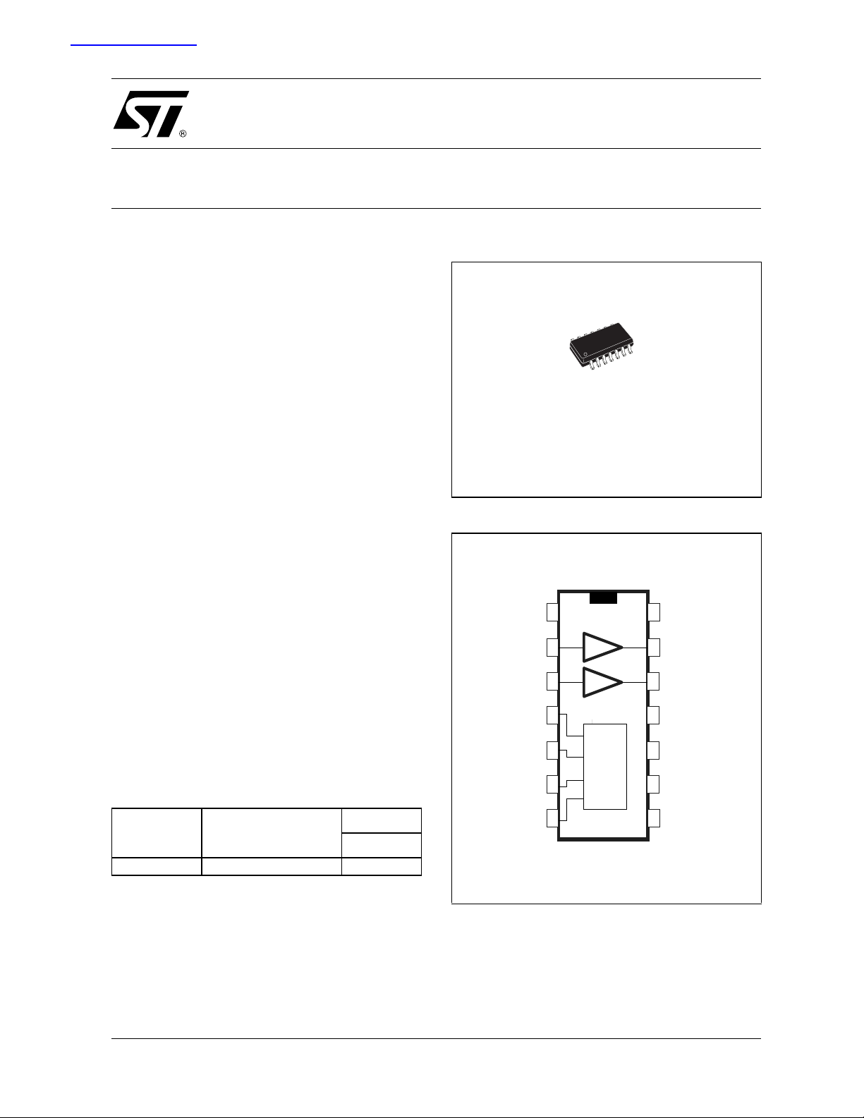
The TS636 comes in SO-14 plastic packages.
D
SO14
(Plastic Micropackage)
PIN CONNECTIONS (top view)
+Vcc1
Inpu t 1
Input 2
1
2
3
14
13
12
+Vcc2
Output 1
Output 2
APPLICATION
■ Preamplifier with automatic gain control for
Asymmetric Digital Subscriber Line (ADSL).
ORDER CODE
Part Number Temperature Range
TS636I -40, +85°C
D = Small Outline Package (SO) - also available in Tape & Reel (DT)
January 2001
Package
D
•
LSB
GC1
GC2
GC3
MSB GC4
4
5
6
Gain Control
7
11
Power Down
10
-Vcc
AGND
9
Logic De coder
8
DGND
1/9
TS636
ABSOLUTE MAXIMUM RATINGS
Symbol Parameter Value Unit
V
T
T
R
R
Supply voltage
CC
V
Input Voltage
i
Operating Free Air Temperature Range TS636ID -40 to + 85 °C
oper
Storage Temperature -65 to +150 °C
std
T
Maximum Junction Temperature 150 °C
j
Thermal Resistance Junction to Case 22 °C/W
thjc
Thermal Resistance Junction to Ambiante Area 125 °C/W
thja
Output Short Circuit Duration Infinite
1. All voltages values are with respect to network terminal.
2. The magnitude of input and output voltages must never exceed V
OPERATING CONDITIONS
Symbol Parameter Value Unit
V
V
Supply Voltage 5 to 12 V
CC
Common Mode Input Voltage
icm
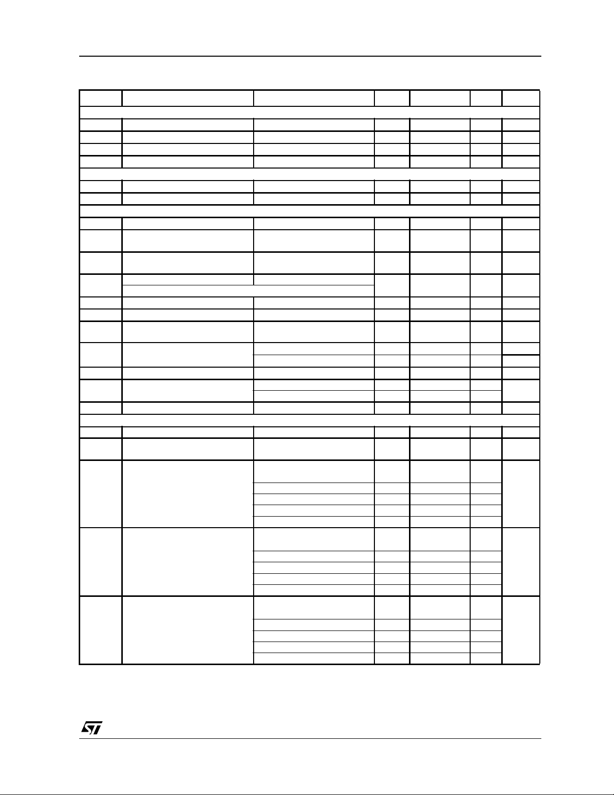
APPLICATION: ADSL LINE INTERFACE
1)
2)
+0.3V.
CC
14 V
0 to 14 V
/2
V
CC
V
ASCOT ADSL
CHIP-SET
ST70135 ST70134
TX
LP filter
emission
(analog
signal)
Power Down
RX
reception
(analog signal)
4-bit Gain Cont rol
TS634 or TS635
Line Driver
VGA
upstream
downstream
TS636
Receiver
HYBRID
CIRCUIT
twisted-pair
telephone
line
2/9
TS636
ELECTRICAL CHARACTERISTICS. VCC = ±6Volts, T
= 25°C (unless otherwise specified).
amb
Symbol Parameter Test Condition Min. Typ. Max Unit
DC PERFORMANCE
I
Input Bias Current (AGND pin) 8
ib
I
Total Supply Current
CC
V
∆
OFFSET
Differential Input Offset Voltage
SVR Supply Voltage Rejection Ratio
No load, V
V
= 0, AV = 30dB
in
A
= 0dB
V
out
= 0
28 mA
6mV
50 80 dB
POWER DOWN MODE
I
ccpdw
Z
Power Down Total Consumption Power Down Mode 150
Power Down Output Impedance Power Down Mode 100kΩ150kΩ//5pF
out
AC PERFORMANCE
Z
Input Impedance 100kΩ//5pF
in
V
V
P
A
A
R
High Level Output Voltage
OH
OL
A
V
AV
vstep
vmis
B
w
bw
I
o
connected to GND
R
L
Low Level Output Voltage
R
connected to GND
L
Voltage Gain F= 1MHz
Gain monotonicity guaranteed by design
Precision of the Voltage Gain F= 1MHz -1.4 1.4 dB
Step Value F= 1MHz 2.4 3 3.6 dB
Gain Mismatch between Both
Channels
Bandwidth @ -3dB
R
= 500Ω, CL = 15pF
L
Bandwidth Roll-off
Bandwidth @ -3dB
= 500Ω, CL = 15pF
R
L
SR Slew Rate (gain independent)
= 500
R
R
L
= 500
L
Ω
Ω
4 4.5 V
-4.5 -4 V
-9 30 dB
F= 1MHz 1 dB
A
= -9dB
V
= +30dB
A
V
A
= +30dB, F = 1MHz
V
45 100 MHz
917 MHz
0.08 dB
|Source| 17 28
Sink 17 22
V
= 2Vpeak
o
40 90 V/µs
NOISE AND DISTORTION
in Equivalent Input Noise Current F = 100kHz 1.6 pA/√Hz
en Equivalent Input Noise Voltage
THD30 Harmonic Distorsion
Third Order Intermodulation
IM3_1
Product
F1 = 180kHz, F2 = 280kHz
Third Order Intermodulation
IM3_2
Product
F1 = 70kHz, F2 = 80kHz
F = 100kHz
= 30dB
A
V
1Vpeak, F = 150kHz,
= +30dB, RL = 500Ω//15pF
A
V
H2 -70
H3 -93
H4 -98
H5 -99
= 1Vpeak, AV = +30dB
V
out
= 500Ω//15pF
R
L
@ 80kHz -77
@ 380kHz -85
@640kHz -86
@740kHz -87
= 1Vpeak, AV = +30dB
V
out
= 500Ω//15pF
R
L
@ 60kHz -77
@ 90kHz -79
@220kHz -83
@230kHz -84
4.7 nV/√Hz
µ
µ
mA
dBc
dBc
dBc
A
A
3/9
 Loading...