


查询TS634供应商
DUAL WIDE BAND OPERATIONAL AMPLIFIER
■ LOW NOISE : 3.2nV/√Hz, 1.5pA/√Hz
■ HIGH OUTPUT CURRENT : 160mA min.
■ VERY LOW HARMONIC AND INTERMODU-
LATION DISTO RTION
■ HIGH SLEW RATE : 40V/µs
TS634
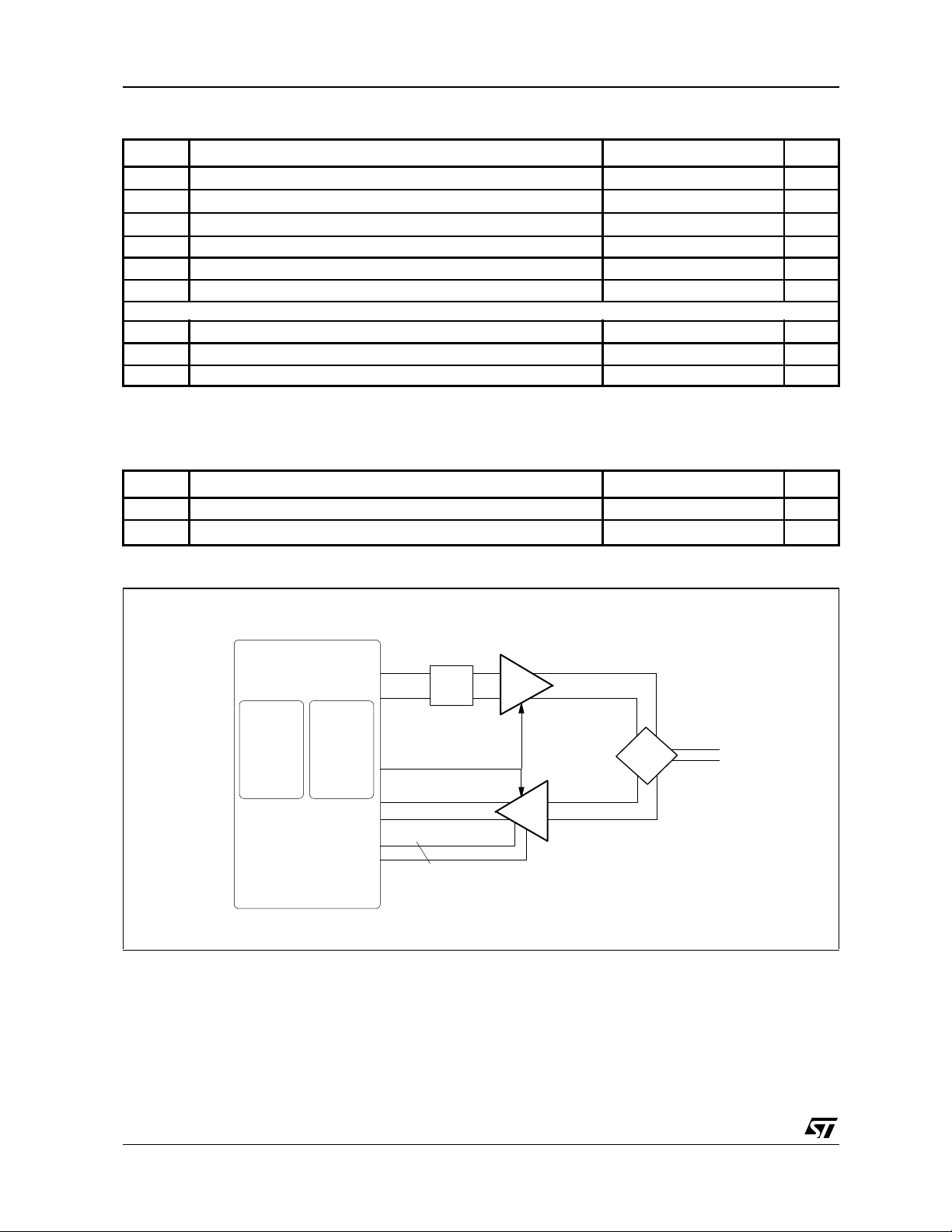
FOR ADSL LINE INTERFACE
■ SPECIFIED FOR 25Ω LOAD
DESCRIPTION
This device is particularly intended for applications
where multiple carriers must be amplified simultaneously with very low intermodulation products. It
has been mainly designed to fit with ADSL
chip-set such as ST70134 or ST70135.
The TS634 is a high output current dual operational amplifier, with a large gain-band width product
(130MHz) and capable of driving a 25Ω load at
12V power supply. The TS634 is fitted out with
Power Down function in order to decrease the
consumption.
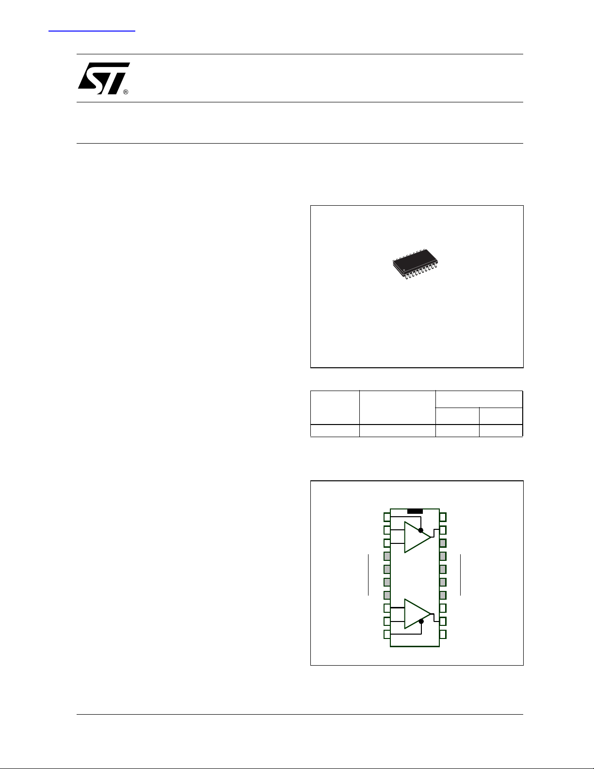
The TS634 is housed in SO20 batwing plastic
package for a very low thermal resistance.
APPLICATION
■ UPSTREAM line driver for Asymmetric Digital
Subscri ber Line (ADSL) (NT).
D
SO20 Batwing
(Plastic Micropackage)
ORDER CODE
Part
Number
Temperature
Range
TS634ID -40, +85°C
D=Small Outline Package (SO) - also available in Tape & Reel (DT)
Package
DP
•
PIN CONNECTIONS (top view)
SO20 batwing - To p V iew
Power Down 1
Inverting input 1
Non-inver ting i nput 1
Thermal Heat Tabs
connected to -Vcc
Non-Inverting i nput 2
Inverting input 2
Power Down 2
Vcc -
Vcc -
Vcc -
Vcc -
1
_
2
3
+
4
5
6
7
8
+
_
9
10
20
19
18
17
16
15
14
13
12
11
Vcc+ 1
Output 1
Vcc-
Vcc -
Vcc -
Vcc -
Vcc -
GND
Output 2
Vcc+ 2
Thermal Heat Tabs
connected to -Vcc
March 2003
1/9
TS634
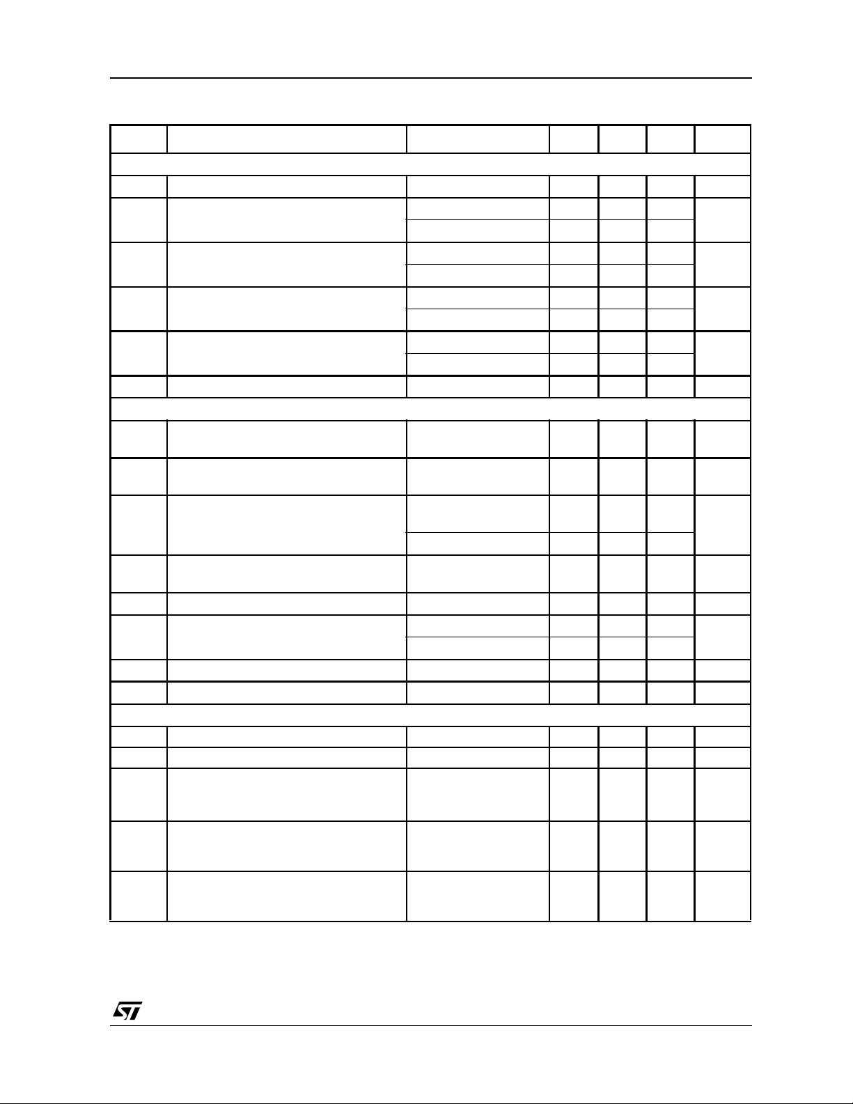
ABSOLUTE MAXIMUM RATINGS
Symbol Parameter Value Unit
V
T
T
Supply voltage
CC
V
Differential Input Voltage
id
V
Input Voltage Range
in
Operating Free Air Temperature Range TS634TS634ID -40 to +85 °C
oper
Storage Temperature -65 to +150 °C
std
T
Maximum Junction Temperature 150 °C
j
SO20-Batwing
R
R
P
1. All voltages values, except differential voltage are with respect to network terminal.
2. Differential voltages are non-inverting input terminal with respect to the inverting input terminal.
3. The magnitude of input and output voltages must never exceed V
Thermal Resistance Junction to Case 25 °C/W
thjc
Thermal Resistance Junction to Ambient Area 45 °C/W
thja
Maximum Power Dissipation (@25°C) 2.7 W
max.
OPERATING CONDITIONS
Symbol Parameter Value Unit
V
V
Supply Voltage ±2.5 to ±6 V
CC
Common Mode Input Voltage
icm
1)
2)
3)
+0.3V.
CC
(V
±7 V
±2 V
±6 V
) +2 to (V
CC
CC
+
) -1
V
APPLICATION: ADSL LINE INTERFACE
ASCOT ADSL
CHIP-SET
ST70135 ST70134
TX
emission
(analog
signal)
Power Down
RX
reception
(analog signal)
LP filter
4-bit Gain C ontrol
TS634
Line Driver
upstream
VGA
TS636
Receiver
downstream
HYBRID
CIRCUIT
twisted-pa ir
telephone
line
2/9
TS634
ELECTRICAL CHARACTERISTICS VCC = ±6Volts, T
= 25°C (unless otherwise specified)
amb
Symbol Parameter Test Condition Min. Typ. Max. Unit
DC PERFORMANCE
V
∆
Differential Input Offset Voltage
io
I
Input Offset Current
io
I
Input Bias Current
ib
CMR Common Mode Rejection Ratio
SVR Supply Voltage Rejection Ratio
I
Total Supply Current per Operator
CC
T
= 25°C
amb
T
amb
< T
< T
< T
< T
amb
amb
amb
amb
< T
< T
< T
< T
out
T
min.
T
amb
T
min.
= 2V to 2V, T
V
ic
T
min.
= ±6V to ±4V, T
V
ic
T
min.
No load, V
= 0
max.
max.
amb
max.
max.
amb
6mV
0.2 3
5
515
30
90 108
70
70 88
50
14 mA
DYNAMIC PERFORMANCE
I
= 160mA
V
High Level Output Voltage
OH
V
Low Level Output Voltage
OL
A
Large Signal Voltage Gain
VD
GBP Gain Bandwidth Product
SR Slew Rate
I
sink
I
source
Φ
Φ
Output Current
Phase Margin at A
M14
Phase Margin at A
M6
VCL
VCL
= 14dB RL = 25Ω//15pF
= 6dB RL = 25Ω//15pF
out
connected to GND
R
L
I
= 160mA
out
connected to GND
R
L
= 7V peak
V
out
R
= 25Ω, T
L
T
min.
A
VCL
= 100
R
L
A
VCL
= ±1V, T
V
id
T
min.
amb
< T
< T
amb
= +7, f = 20MHz
Ω
= +7, RL = 50
amb
< T
< T
amb
4 4.5 V
-4.5 -4 V
6500 11000
max.
5000
130 MHz
Ω
max.
23 40 V/µs
160
140
60 °
40 °
NOISE AND DISTORTION
en Equivalent Input Noise Voltage f = 100kHz 3.2 nV/√Hz
in Equivalent Input Noise Current f = 100kHz 1.5 pA/√Hz
V
= 4Vpp, f = 100kHz
out
A
THD Total Harmonic Distortion
IM2
IM3
2nd Order Intermodulation Product
-10
3rd Order Intermodulation Produ ct
-10
= -10
VCL
= 25Ω//15pF
R
L
F1 = 80kHz, F2 = 70kHz
= 8Vpp, A
V
out
VCL
= -10
Load = 25Ω//15pF
F1 = 80kHz, F2 = 70kHz
= 8Vpp, A
V
out
VCL
= -10
Load = 25Ω//15pF
-69 dB
-77 dBc
-77 dBc
A
µ
A
µ
dB
dB
V/V
mA
3/9