

Page 1

Features
■ Low noise: 2.5 nV/√Hz
■ High output current: 420 mA
■ Very low harmonic and intermodulation
distortion
■ High slew rate: 420 V/µs
■ -3dB bandwidth: 40 MHz @ gain = 12 dB on
25 Ω single-ended load
■ 20.7 Vp-p differential output swing on 50 Ω
load, 12 V power supply
■ Current feedback structure
■ 5 V to 12 V power supply
■ Specified for 20 Ω and 50 Ω differential load
Applications
■ Line driver for xDSL
■ Multiple video line driver
TS616
Dual wide band operational amplifier
with high output current
DW
SO-8 Exposed-pad
(Plastic micropackage)
Pin connections (top view)
Output1
Output1
1
1
2
Inverting Input1 Output2
Inverting Input1 Output2
Non Inverting Input1
Non Inverting Input1
This pad must be connected to a (-Vcc) copper area on the PCB
This pad must be connected to a (-Vcc) copper area on the PCB
2
-
-
+
+
3
3
VCC -
VCC -
4
4
Cross Section View Showing Exposed-Pad.
Cross Section View Showing Exposed-Pad.
VCC +
VCC +
8
8
7
7
Inverting Input2
Inverting Input2
6
6
-
-
+
+
Non Inverting Input2
Non Inverting Input2
5
5
dice
dice
Pad
Pad
Description
The TS616 is a dual operational amplifier
featuring a high output current of 410 mA. This
driver can be configured differentially for driving
signals in telecommunication systems using
multiple carriers. The TS616 is ideally suited for
xDSL (high speed asymmetrical digital subscriber
line) applications. This circuit is capable of driving
a 10 Ω or 25 Ω load on a range of power supplies:
±2.5 V, 5 V, ±6 V or +12 V. The TS616 is capable
of reaching a -3 dB bandwidth of 40 MHz on 25 Ω
load with a 12 dB gain. This device is designed for
high slew rates and demonstrates low harmonic
distortion and intermodulation.
September 2008 Rev 5 1/37
www.st.com
37
Page 2

Contents TS616
Contents
1 Typical application . . . . . . . . . . . . . . . . . . . . . . . . . . . . . . . . . . . . . . . . . . 3
2 Absolute maximum ratings and operating conditions . . . . . . . . . . . . . 4
3 Electrical characteristics . . . . . . . . . . . . . . . . . . . . . . . . . . . . . . . . . . . . . 5
4 Safe operating area . . . . . . . . . . . . . . . . . . . . . . . . . . . . . . . . . . . . . . . . . 16
5 Intermodulation distortion product . . . . . . . . . . . . . . . . . . . . . . . . . . . . 17
6 Printed circuit board layout considerations . . . . . . . . . . . . . . . . . . . . . 20
6.1 Thermal information . . . . . . . . . . . . . . . . . . . . . . . . . . . . . . . . . . . . . . . . . 20
7 Noise measurements . . . . . . . . . . . . . . . . . . . . . . . . . . . . . . . . . . . . . . . 23
7.1 Measurement of eN . . . . . . . . . . . . . . . . . . . . . . . . . . . . . . . . . . . . . . . . . 24
7.2 Measurement of iNn . . . . . . . . . . . . . . . . . . . . . . . . . . . . . . . . . . . . . . . . . 25
7.3 Measurement of iNp . . . . . . . . . . . . . . . . . . . . . . . . . . . . . . . . . . . . . . . . . 25
8 Power supply bypassing . . . . . . . . . . . . . . . . . . . . . . . . . . . . . . . . . . . . 26
8.1 Single power supply . . . . . . . . . . . . . . . . . . . . . . . . . . . . . . . . . . . . . . . . . 26
8.2 Channel separation and crosstalk . . . . . . . . . . . . . . . . . . . . . . . . . . . . . . 27
9 Choosing the feedback circuit . . . . . . . . . . . . . . . . . . . . . . . . . . . . . . . . 28
9.1 The bias of an inverting amplifier . . . . . . . . . . . . . . . . . . . . . . . . . . . . . . . 29
9.2 Active filtering . . . . . . . . . . . . . . . . . . . . . . . . . . . . . . . . . . . . . . . . . . . . . . 29
10 Increasing the line level using active impedance matching . . . . . . . . 31
11 Package information . . . . . . . . . . . . . . . . . . . . . . . . . . . . . . . . . . . . . . . . 34
12 Ordering information . . . . . . . . . . . . . . . . . . . . . . . . . . . . . . . . . . . . . . . 36
13 Revision history . . . . . . . . . . . . . . . . . . . . . . . . . . . . . . . . . . . . . . . . . . . 36
2/37
Page 3
TS616 Typical application
1 Typical application
Figure 1 shows a schematic of a typical xDSL application using the TS616.
Figure 1. Differential line driver for xDSL applications
8
8
3
3
2
2
Vi
Vi
Vi
Vi
R1
R1
R4
R4
Vi Vo
Vi Vo
Vi Vo
Vi Vo
4
4
5
5
+
+
+
+
1/2TS61 5
1/2TS61 6
1/2TS61 5
1/2TS61 6
_
_
_
_
R2
R2
GND
GND
R3
R3
_
_
_
_
1/2TS615
1/2TS616
1/2TS615
1/2TS616
+
+
+
+
4
4
+Vcc
+Vcc
+Vcc
+Vcc
-Vcc
-Vcc
-Vcc
-Vcc
Ω
Ω
Ω
Ω
12.5
12.5
12.5
12.5
1
1
1
1
Vo
Vo
Vo
12.5
12.5
12.5
12.5
Vo
Ω
Ω
Ω
Ω
25
25
25
25
1:2
1:2
1:2
1:2
Ω
Ω
Ω
Ω
Ω
Ω
Ω
100
100
100
100
Ω
3/37
Page 4

Absolute maximum ratings and operating conditions TS616
2 Absolute maximum ratings and operating conditions
Table 1. Absolute maximum ratings
Symbol Parameter Value Unit
V
CC
V
id
V
in
T
oper
T
std
T
j
R
thjc
R
thja
P
max
ESD
only pins
1, 4, 7, 8
ESD
only pins
2, 3, 5, 6
Supply voltage
Differential input voltage
Input voltage range
Operating free air temperature range -40 to + 85 °C
Storage temperature -65 to +150 °C
Maximum junction temperature 150 °C
Thermal resistance junction to case 16 °C/W
Thermal resistance junction to ambient area 60 °C/W
Maximum power dissipation (at T
=150°C
T
j
HBM: human body model
MM: machine model
CDM: charged device model
HBM: human body model
MM: machine model
CDM: charged device model
Output short circuit
(1)
(3)
(5)
(5)
(2)
(4)
(4)
(6)
(6)
= 25° C) for
amb
±7 V
±2 V
±6 V
2W
1.5
2
200
1.5
2
100
(7)
kV
kV
V
kV
kV
V
1. All voltage values, except differential voltage are with respect to network terminal.
2. Differential voltages are non-inverting input terminal with respect to the inverting input terminal.
3. The magnitude of input and output voltage must never exceed VCC +0.3 V.
4. Human body model: a 100 pF capacitor is charged to the specified voltage, then discharged through a
1.5 kΩ resistor between two pins of the device. This is done for all couples of connected pin combinations
while the other pins are floating.
5. Machine model: a 200 pF capacitor is charged to the specified voltage, then discharged directly between
two pins of the device with no external series resistor (internal resistor < 5 Ω). This is done for all couples of
connected pin combinations while the other pins are floating.
6. Charged device model: all pins and the package are charged together to the specified voltage and then
discharged directly to the ground through only one pin. This is done for all pins.
7. An output current limitation protects the circuit from transient currents. Short-circuits can cause excessive
heating. Destructive dissipation can result from short-circuits on amplifiers.
Table 2. Operating conditions
Symbol Parameter Value Unit
V
CC
V
icm
Power supply voltage ±2.5 to ±6 V
Common mode input voltage -VCC+1.5 V to +VCC-1.5 V V
4/37
Page 5
TS616 Electrical characteristics
3 Electrical characteristics
Table 3. V
= ±6 V, Rfb= 910 Ω, T
CC
= 25° C (unless otherwise specified)
amb
Symbol Parameter Test conditions Min. Typ. Max. Unit
DC performance
V
io
ΔV
I
ib+
I
ib-
Z
IN+
Z
IN-
C
IN+
CMR
SVR
I
CC
T
Input offset voltage
Differential input offset voltage T
io
Positive input bias current
Negative input bias current
amb
< T
T
T
T
T
T
min
amb
amb
min
amb
min
< T
amb
max
= 25°C 2.5 mV
530
< T
< T
amb
max
315
< T
< T
amb
max
Input(+) impedance 82 kΩ
Input(-) impedance 54 Ω
Input(+) capacitance 1 pF
ΔV
Common mode rejection ratio
20 log (ΔV
/ΔVio)
ic
Supply voltage rejection ratio
20 log (ΔVCC/ΔVio)
= ±4.5V 58 64
ic
< T
T
ΔV
T
min
CC
min
< T
amb
max
= ±2.5V to ±6V 72 81
< T
< T
amb
max
Total supply current per operator No load 13.5 17 mA
13.5
1.6
7.2
3.1
62
80
Dynamic performance and output characteristics
mV
µA
µA
dB
dB
R
Open loop transimpedance
OL
-3dB bandwidth
BW
Full power bandwidth
Gain flatness @ 0.1dB
Rise time V
T
r
T
Fall time V
f
Settling time V
T
s
SR Slew rate V
V
V
High level output voltage RL = 25Ω connected to GND 4.8 5.05 V
OH
Low level output voltage RL = 25Ω Connected to GND -5.3 -5.1 V
OL
V
= 7Vp-p, RL = 25Ω 513.5
out
< T
T
min
Small signal V
= 12dB, RL = 25Ω
A
V
Large signal V
= 12dB, RL = 25Ω
A
V
Small signal T
amb
< T
max
< 20mVp
out
= 3Vp
out
<20mVp
amb
AV = 12dB, RL = 25Ω
= 6Vp-p, AV = 12dB, RL = 25Ω 10.6 ns
out
= 6Vp-p, AV = 12dB, RL = 25Ω 12.2 ns
out
= 6Vp-p, AV= 12dB, RL = 25Ω 50 ns
out
= 6Vp-p, AV = 12dB, RL = 25Ω 330 420 V/µs
out
5.7
25 40
26
7MHz
5/37
MΩ
MHz
Page 6

Electrical characteristics TS616
Table 3. V
= ±6 V, Rfb= 910 Ω, T
CC
= 25° C (unless otherwise specified) (continued)
amb
Symbol Parameter Test conditions Min. Typ. Max. Unit
V
= -4Vp -320 -490
Output sink current
I
out
Output source current
out
T
< T
< T
amb
amb
< T
< T
max
max
min
V
= +4Vp 330 420
out
T
min
-395
370
Noise and distortion
eN Equivalent input noise voltage F = 100kHz 2.5 nV/√Hz
iNp Equivalent input noise current (+) F = 100kHz 15 pA/√Hz
iNn Equivalent input noise current (-) F = 100kHz 21 pA/√Hz
HD2
HD3
2nd harmonic distortion
(differential configuration)
3rd harmonic distortion
(differential configuration)
V
= 14Vp-p, AV = 12dB
out
F= 110kHz, RL = 50Ω diff.
= 14Vp-p, AV = 12dB
V
out
F= 110kHz, R
= 50Ω diff.
L
-87 dBc
-83 dBc
F1= 100kHz, F2 = 110kHz
IM2
2nd order intermodulation product
(differential configuration)
= 16Vp-p, AV = 12dB
V
out
RL = 50Ω diff.
F1= 370kHz, F2 = 400kHz
= 16Vp-p, AV = 12dB
V
out
-76
-75
RL = 50Ω diff.
F1 = 100kHz, F2 = 110kHz
IM3
3rd order intermodulation product
(differential configuration)
= 16Vp-p, A
V
out
RL = 50Ω diff.
F1 = 370kHz, F2 = 400kHz
= 16Vp-p, A
V
out
= 12dB
V
= 12 B
V
-88
-87
RL = 50Ω diff.
mA
dBc
dBc
6/37
Page 7

TS616 Electrical characteristics
Table 4. VCC = ±2.5 V, Rfb= 910 Ω, T
= 25° C (unless otherwise specified)
amb
Symbol Parameter Test conditions Min. Typ. Max. Unit
DC performance
T
0.2 2.5
V
io
ΔV
I
ib+
I
ib-
Z
IN+
Z
IN-
C
IN+
CMR
SVR
I
CC
Input offset voltage
Differential input offset voltage T
i
o
Positive input bias current
Negative input bias current
Input(+) impedance 71 kΩ
Input(-) impedance 62 Ω
Input(+) capacitance 1.5 pF
Common mode rejection ratio
20 log (ΔV
/ΔVio)
ic
Supply voltage rejection ratio
20 log (ΔV
cc
/ΔVio)
Total supply current per
operator
amb
< T
T
T
T
T
T
ΔV
T
ΔV
T
min
amb
amb
min
amb
min
ic
min
CC
min
< T
amb
max
= 25°C 2.5 mV
430
< T
< T
amb
max
1.1 11
< T
< T
amb
max
= ±1V 55 61
< T
< T
amb
max
= ±2V to ±2.5V 63 79
< T
< T
amb
max
1
7
1.2
60
78
No load 11.5 15 mA
mV
µA
µA
dB
dB
Dynamic performance and output characteristics
V
= 2V
R
Open loop transimpedance
OL
-3dB bandwidth
BW
Full power bandwidth
Gain flatness @ 0.1dB
Rise time V
T
r
Fall time V
T
f
T
Settling time V
s
SR Slew rate V
V
V
High level output voltage RL=10Ω connected to GND 1.5 1.7 V
OH
Low level output voltage RL=10Ω connected to GND -1.9 -1.7 V
OL
Output sink current
I
out
Output source current
out
< T
T
min
Small signal V
AV = 12dB, RL = 10Ω
Large signal V
R
= 10Ω
L
Small signal V
= 12dB, RL = 10Ω
A
V
= 2.8Vp-p, AV = 12dB RL= 10Ω 11 ns
out
= 2.8Vp-p, AV = 12dB RL= 10Ω 11.5 ns
out
= 2.2Vp-p, AV = 12dB RL= 10Ω 39 ns
out
= 2.2Vp-p, AV = 12dB RL =10Ω 100 130 V/µs
out
V
= -1.25V
out
T
< T
min
V
= +1.25V
out
< T
T
min
, RL = 10Ω 24.2
p-p
< T
amb
max
< 20mVp
amb
amb
out
= 1.4Vp AV=12dB,
out
< 20mVp
out
p
< T
max
p
< T
max
20 28
-300 -400
-360
200 270
1.5
MΩ
MHz
20
5.7 MHz
mA
240
7/37
Page 8

Electrical characteristics TS616
Table 4. VCC = ±2.5 V, Rfb= 910 Ω, T
= 25° C (unless otherwise specified) (continued)
amb
Symbol Parameter Test conditions Min. Typ. Max. Unit
Noise and distorsion
eN Equivalent input noise voltage F = 100kHz 2.5 nV/√Hz
iNp
iNn
HD2
HD3
Equivalent input noise current
(+)
Equivalent input noise current
(-)
2nd harmonic distortion
(differential configuration)
3rd harmonic distortion
(differential configuration)
F = 100kHz 15 pA/√Hz
F = 100kHz 21 pA/√Hz
= 6V
V
out
F= 110kHz, RL = 20 Ω diff.
V
= 6V
out
F= 110 kHz, RL = 20Ω diff.
, AV = 12 dB
p-p
, AV = 12dB
p-p
-97 dBc
-98 dBc
F1= 100 kHz, F2 = 110 kHz
IM2
2nd order intermodulation
product
(differential configuration)
= 6 V
V
out
RL = 20Ω diff.
F1= 370kHz, F2 = 400kHz
= 6V
V
out
, AV = 12dB
p-p
, AV = 12dB
p-p
-86
-88
RL = 20Ω diff.
F1 = 100kHz, F2 = 110kHz
V
IM3
3rd order intermodulation
product
(differential configuration)
= 6V
out
RL = 20Ω diff.
F1 = 370kHz, F2 = 400kHz
= 6V
V
out
p-p
p-p
, A
, A
= 12dB
V
= 12dB
V
-90
-85
RL = 20Ω diff.
dBc
dBc
8/37
Page 9

TS616 Electrical characteristics
Figure 2. Load configuration Figure 3. Load configuration
RL= 25Ω
VCC= ±6 V
+
+
TS616
TS616
_
_
+6V
+6V
-6V
-6V
25Ω
25Ω
49.9Ω
49.9Ω
33Ω
33Ω
1W
1W
50Ω
50Ω
cable
cable
50Ω
50Ω
RL= 25 Ω
VCC= ±.5V
+
+
TS616
TS616
_
_
+2.5V
+2.5V
-2.5V
-2.5V
10Ω
10Ω
49.9Ω
49.9Ω
11Ω
11Ω
0.5W
0.5W
50Ω
50Ω
cable
cable
Figure 4. Closed loop gain vs. frequency Figure 5. Closed loop gain vs. frequency
AV=+1, VCC=±2.5V, Rfb=1.1kΩ, RL=10Ω
VCC=±6V, Rfb=750Ω, RL=25Ω
2
0
-2
-4
-6
-8
(gain (dB)
-10
-12
-14
-16
100 1k 10k 100k 1M 10M 100M
gain
phase
Frequency (Hz)
(Vcc=±6V)
(Vcc=±2.5V)
(Vcc=±2.5V)
(Vcc=±6V)
40
20
0
-20
-40
-60
-80
-100
-120
AV=-1, VCC= ±2.5V, Rfb=1kΩ, Rin=1kΩ, RL=10Ω
VCC=±6V, Rfb=680Ω, Rin=680Ω, RL=25Ω
2
0
-2
-4
-6
-8
Phase (°)
(gain (dB))
-10
-12
-14
-16
100 1k 10k 100k 1M 10M 100M
gain
phase
Frequency (Hz)
(Vcc=±2.5V)
(Vcc=±6V)
(Vcc=±2.5V)
(Vcc=±6V)
50Ω
50Ω
-140
-160
-180
-200
-220
-240
-260
-280
-300
Phase (°)
Figure 6. Closed loop gain vs. frequency Figure 7. Closed loop gain vs. frequency
AV=+2, VCC=±2.5V, Rfb=1kΩ, RL=10Ω
VCC=±6V, Rfb=680Ω, RL=25Ω
8
6
4
2
0
-2
(gain (dB))
-4
-6
-8
-10
100 1k 10k 100k 1M 10M 100M
gain
phase
(Vcc=±2.5V)
Frequency (Hz)
(Vcc=±6V)
(Vcc=±2.5V)
(Vcc=±6V)
AV=-2, VCC=±2.5V, Rfb=1kΩ, Rin=510Ω, RL=10Ω
40
20
0
-20
-40
-60
-80
-100
-120
VCC=±6V, Rfb=680Ω, Rin=750/620Ω, RL=25Ω
8
6
4
2
0
-2
Phase (°)
(gain (dB))
-4
-6
-8
-10
100 1k 10k 100k 1M 10M 100M
gain
phase
(Vcc=±2.5V)
Frequency (Hz)
(Vcc=±2.5V)
(Vcc=±6V)
(Vcc=±6V)
9/37
-140
-160
-180
-200
-220
-240
-260
-280
-300
Phase (°)
Page 10

Electrical characteristics TS616
Figure 8. Closed loop gain vs. frequency Figure 9. Closed loop gain vs. frequency
=+4, VCC=±2.5V, Rfb=910Ω, Rg=300Ω, RL=10Ω
V
VCC=±6V, Rfb=620Ω, Rg=560/330
14
12
10
8
6
4
(gain (dB))
2
0
-2
-4
100 1k 10k 100k 1M 10M 100M
gain
phase
(Vcc=±2.5V)
Frequency (Hz)
Ω,
(Vcc=±2.5V)
(Vcc=±6V)
(Vcc=±6V)
RL=25
Ω
AV=-4, VCC=±2.5V, Rfb=1kΩ Rin=320/360Ω RL=10Ω
40
20
0
-20
-40
-60
-80
-100
-120
VCC=±6V, Rfb=620
14
12
10
8
6
Phase (°)
4
(gain (dB))
2
0
-2
-4
100 1k 10k 100k 1M 10M 100M
Ω,
Rin=360/270
gain
phase
Frequency (Hz)
(Vcc=±2.5V)
(Vcc=±2.5V)
(Vcc=±6V)
Ω,
RL=25
(Vcc=±6V)
Ω
Figure 10. Closed loop gain vs. frequency Figure 11. Closed loop gain vs. frequency
AV=+8, VCC=±2.5V, Rfb=680Ω,Rg=240/160Ω,RL=10Ω
VCC=±6V, Rfb=510
20
18
16
14
12
10
(gain (dB))
8
6
4
2
100 1k 10k 100k 1M 10M 100M
Ω,
Rg=270/100
gain
phase
Frequency (Hz)
(Vcc=±2.5V)
(Vcc=±2.5V)
(Vcc=±6V)
Ω,
RL=25
(Vcc=±6V)
Ω
40
20
0
-20
-40
-60
-80
-100
-120
AV=-8, VCC=±2.5V, Rfb=680Ω Rin=160/180Ω RL=10Ω
VCC=±6V, Rfb=510
20
18
16
14
12
10
Phase (°)
(gain (dB))
8
6
4
2
100 1k 10k 100k 1M 10M 100M
Ω,
Rin=150/110
gain
phase
Frequency (Hz)
(Vcc=±2.5V)
(Vcc=±2.5V)
(Vcc=±6V)
Ω,
RL=25
(Vcc=±6V)
Ω
-140
-160
-180
-200
-220
-240
-260
-280
-300
-140
-160
-180
-200
-220
-240
-260
-280
-300
Phase (°)
Phase (°)
Figure 12. Positive slew rate Figure 13. Positive slew rate
AV = +4, Rfb = 910Ω, VCC = ±6 , RL=25Ω
4
2
(V)
0
OUT
V
-2
-4
0.0 10 .0n 20.0n 30.0n 40.0n 50.0n
Time (s)
10/37
AV = +4, Rfb = 910 Ω, VCC = ±2.5V, RL=10Ω
2
1
(V)
0
OUT
V
-1
-2
0.0 10. 0n 20.0n 30.0n 40.0n 50.0n
Time (s)
Page 11

TS616 Electrical characteristics
Figure 14. Positive slew rate Figure 15. Positive slew rate
AV = -4, Rfb = 620 Ω, VCC = ±6 V, RL=25Ω
4
2
(V)
0
OUT
V
-2
-4
0.0 10. 0n 20.0n 30.0n 40.0n 50.0n
Time (s)
AV = -4, Rfb = 910 Ω, VCC = ±2.5 V, RL=10Ω
2
1
(V)
0
OUT
V
-1
-2
0.0 10. 0n 20.0n 30.0n 40.0n 50.0n
Time (s)
Figure 16. Negative slew rate Figure 17. Negative slew rate
AV = +4, Rfb = 620 Ω, VCC = ±6 V, RL=25Ω
4
2
AV = +4, Rfb = 910 Ω, VCC = ±2.5 V, RL=10Ω
2
1
(V)
0
OUT
V
-2
-4
0.0 10. 0n 20.0n 30.0n 40.0n 50.0n
Time (s)
(V)
0
OUT
V
-1
-2
0.0 10. 0n 20.0n 30.0n 40.0n 50.0n
Time (s)
Figure 18. Negative slew rate Figure 19. Negative slew rate
AV = +4, Rfb = 620 Ω, VCC = ±6 V, RL=25Ω
4
2
(V)
0
OUT
V
-2
-4
0.0 10 .0n 20.0n 30.0n 40.0n 50.0n
Time (s)
AV = +4, Rfb = 910 Ω, VCC = ±2.5 V, RL=10Ω
2
(V)
0
OUT
V
-2
0.0 10. 0n 20.0n 30.0n 40.0n 50.0n
Time (s)
11/37
Page 12

Electrical characteristics TS616
Figure 20. Input voltage noise level Figure 21. ICC vs. power supply
AV = +92, Rfb = 910 Ω
Input+ connected to GND via 25 Ω
5.0
+
+
+
4.5
4.0
3.5
3.0
Input Voltage Noise (nV/√Hz)
2.5
2.0
100 1k 10k 100k 1M
(Frequency (Hz)
+
_
_
_
_
10
10
10
10
+ 6V
+ 6V
+ 6V
+ 6V
Output
Output
Output
Output
6VΩ-
6VΩ-
- 6V
- 6V
910
910
Ω
Ω
910
910
Ω
Ω
Ω
Ω
Open loop, no load
30
20
10
0
(mA)
CC
I
-10
-20
-30
0123456789101112
Icc(+)
Icc(-)
VCC (V)
Figure 22. Iib vs. power supply Figure 23. VOH & VOL vs. power supply
Open loop, no load
7
7
Iib+
Iib+
IB+
IB+
6
6
5
5
4
4
(μA)
(μA)
B
B
3
3
I
I
ib
I
Iib-
IB-
IB-
2
2
1
1
0
0
5 6 7 8 9 10 11 12
5 6 7 8 9 10 11 12
Vcc (V)
Vcc (V)
Open loop, RL = 25 Ω
6
5
4
3
2
(V)
1
OL
0
& V
-1
OH
V
-2
-3
-4
-5
-6
56789101112
VOH
VOL
Vcc (V)
Figure 24. I
source
vs. output amplitude Figure 25. I
VCC = ±6 V, open loop, no load
700
600
500
400
300
Isource (mA)
200
100
0
0123456
Vout (V)
12/37
vs. output amplitude
source
VCC = ±2.5 V, open loop, no load
700
600
500
400
300
Isource (mA)
200
100
0
0.0 0.5 1.0 1.5 2.0 2.5
Vout (V)
Page 13

TS616 Electrical characteristics
Figure 26. I
VCC = ±6 V, open loop, no load
Isink (mA)
vs. output amplitude Figure 27. I
sink
0
-100
-200
-300
-400
-500
-600
-700
-6 -5 -4 -3 -2 -1 0
Vout (V)
vs. output amplitude
sink
VCC = ±2.5 V, open loop, no load
0
-100
-200
-300
-400
Isink (mA)
-500
-600
-700
-2.5 -2.0 -1.5 -1.0 -0.5 0.0
Vout (V)
Figure 28. Maximum output amplitude vs. load Figure 29. Bandwidth vs. temperature
AV = +4, Rfb = 620 Ω, VCC = ±6 V
12
10
)
8
P-P
(V
6
OUT-MAX
V
4
2
Vcc=±6V
Vcc=±2.5V
AV = +4, Rfb = 910 Ω
50
45
40
35
Bw (MHz)
30
25
Vcc=±6V
Load=25
Vcc=±2.5V
Load=10
Ω
Ω
0
0 50 100 150 200
R
(Ω)
LOAD
20
-40-200 2040 6080
Temperature (°C)
Figure 30. Transimpedance vs. temperature Figure 31. ICC vs. temperature
Open loop
30
25
Vcc=±6V
20
15
(MΩ)
OL
R
10
Vcc=±2.5V
5
0
-40-200 2040 6080
Temperature (°C)
Open loop, no load
14
12
10
Icc(+) for Vcc=±2.5V
8
Icc(+) for Vcc=±6V
6
4
2
0
(mA)
-2
CC
I
-4
-6
Icc(-) for Vcc=±6V
-8
-10
-12
-14
Icc(-) for Vcc=±2.5V
-40 -20 0 20 40 6 0 80
Temperature (°C)
13/37
Page 14

Electrical characteristics TS616
Figure 32. Slew rate vs. temperature Figure 33. Slew rate vs. temperature
AV = +4, Rfb = 910 Ω, VCC = ±6 V, RL=25Ω
600
500
400
300
200
100
-100
-200
Slew Rate (V/μs)
-300
-400
-500
-600
Positive&Negative SR
Ω
Rfb=620
0
-40 -20 0 20 40 60 80
Positive&Negative SR
Ω
Rfb=910
Temperature (°C)
AV = +4, Rfb = 910 Ω, VCC = ±2.5 V, RL=10Ω
200
150
100
Positive SR
50
0
-50
Slew Rate (V/μs)
Negative SR
-100
-150
-200
-40 -20 0 20 40 60 80
Temperature (°C)
Figure 34. Iib(+) vs. temperature Figure 35. Iib(+) vs. temperature
Open loop, no load
8
7
6
5
4
(μA)
3
IB(+)
I
2
1
0
-1
-40-20 0 20406080
Vcc=±6V
Vcc=±2.5V
Temperature (°C)
Open loop, no load
5
4
3
(μA)
IB(-)
2
I
1
0
-40 -20 0 20 40 6 0 80
Temperature (°C)
Vcc=±6V
Vcc=±2.5V
Figure 36. VOH vs. temperature Figure 37. VOL vs. temperature
Open loop
6
5
4
3
(V)
OH
V
2
1
0
-40-200 20406080
Vcc=±6vV
Load=25
Vcc=±2.5V
Load=10
Ω
Ω
Temperature (°C)
14/37
Open loop
0
Vcc=±2.5V
-1
-2
-3
(V)
OL
V
-4
-5
-6
-40-200 2040 6080
Load=10Ω
Vcc=±6V
Ω
Load=25
Temperature (°C)
Page 15

TS616 Electrical characteristics
Figure 38. Differential Vio vs. temperature Figure 39. Vio vs. temperature
Open loop, no load
450
400
350
(μV)
IO
ΔV
300
250
200
-40 -20 0 20 40 6 0 80
Vcc=±6V
Temperature (°C)
Figure 40. I
vs. temperature Figure 41. I
out
Open loop, VCC = ±6 V, RL=10Ω
300
250
200
150
100
Isource
50
0
-50
-100
-150
Iout (mA)
-200
-250
-300
-350
-400
-450
Isink
-40 -20 0 20 40 6 0 80
Temperature (°C)
Vcc=±2.5V
Open loop, no load
2.0
1.5
1.0
(mV)
IO
V
0.5
0.0
-0.5
-40-200 2040 6080
Temperature (°C)
vs. temperature
out
Open loop, VCC = ±2.5 V, RL=25Ω
300
250
200
150
100
50
Isource
0
-50
-100
-150
Iout (mA)
-200
-250
-300
-350
-400
-450
Isink
-40 -20 0 20 40 60 80
Temperature (°C)
Vcc=±6V
Vcc=±2.5V
Figure 42. CMR vs. temperature Figure 43. SVR vs. temperature
Open loop, no load
70
68
66
64
62
60
58
CMR (dB)
56
54
52
50
-40-200 2040 6080
Vcc=±2.5V
Temperature (°C)
Vcc=±6V
Open loop, no load
84
82
80
Vcc=±6V
SVR (dB)
78
76
Vcc=±2.5V
-40-200 2040 6080
Temperature (°C)
15/37
Page 16

Safe operating area TS616
4 Safe operating area
Figure 44 shows the safe operating zone for the TS616. The curve shows the input level vs.
the input frequency—a characteristic curve which must be considered in order to ensure a
good application design. In the dash-lined zone, the consumption increases, and this
increased consumption could do damage to the chip if the temperature increases.
Figure 44. Safe operating area
700
Vcc=+/-6V
Ta=25°C
600
G=12dB
RL=100Ω
500
)
RMS
400
(mV
300
INPUT
V
200
100
SAFE
OPERATING
AREA
0
1M 10M 100M
Frequency (Hz)
16/37
Page 17

TS616 Intermodulation distortion product
5 Intermodulation distortion product
The non-ideal output of the amplifier can be described by the following series, due to a nonlinearity in the input-output amplitude transfer:
V
C0C1VinC2V
out
++ +=
2
in
CnV
n
in
where the single-tone input is V
fundamental, C
is the amplitude of the harmonics of the output signal V
n
=Asinωt, and C0 is the DC component, C1(Vin) is the
in
out
.
A one-frequency (one-tone) input signal contributes to a harmonic distortion. A two-tone
input signal contributes to a harmonic distortion and an intermodulation product.
This intermodulation product, or rather, the study of the intermodulation distortion of a twotone input signal is the first step in characterizing the amplifiers capability for driving multitone signals.
The two-tone input is equal to:
V
A ω1tsin B ω2tsin+=
in
giving:
C0C1A ω1tsin B ω2tsin+()C2A ω1tsin B ω2tsin+()
++ +=
t
2
… CnA ω1tsin B ω2tsin+()
n
In this expression, we can extract distortion terms and intermodulation terms from a single
sine wave: second-order intermodulation terms IM2 by the frequencies (ω
with an amplitude of C2A
(2ω
- ω2), (2ω1+ω2), (−ω1+2ω2) and (ω1+2ω2) with an amplitude of (3/4)C3A3.
1
2
and third-order intermodulation terms IM3 by the frequencies
- ω2) and (ω1+ω2)
1
We can measure the intermodulation product of the driver by using the driver as a mixer via
a summing amplifier configuration. In doing this, the non-linearity problem of an external
mixing device is avoided.
Figure 45. Non-inverting summing amplifier for intermodulation measurements
Vin1
Vin1
50Ω
50Ω
1:√2
1:√2
100Ω
100Ω
Vin1
Vin1
50Ω
50Ω
49.9Ω
49.9Ω
1:√2
1:√2
49.9Ω
49.9Ω
100Ω
100Ω
1kΩ
1kΩ
1kΩ
1kΩ
49.9Ω
49.9Ω
49.9Ω
49.9Ω
1kΩ
1kΩ
1kΩ
1kΩ
300Ω
300Ω
300Ω
300Ω
+
+
1/2TS616
1/2TS616
_
_
910Ω
910Ω
910Ω
910Ω
_
_
1/2TS616
1/2TS616
+
+
+Vcc
+Vcc
-Vcc
-Vcc
Vout diff.
Vout diff.
49.9Ω
49.9Ω
Rout1
Rout1
Rout2
Rout2
49.9Ω
49.9Ω
100Ω
100Ω
√2:1
√2:1
17/37
50Ω
50Ω
Page 18

Intermodulation distortion product TS616
The following graphs show the IM2 and the IM3 of the amplifier in different configurations.
The two-tone input signal was generated by the multisource generator Marconi 2026. Each
tone has the same amplitude. The measurement was performed using a HP3585A
spectrum analyzer.
Figure 46. Intermodulation vs. output
amplitude
Figure 47. Intermodulation vs. output
amplitude
370 kHz & 400 kHz
AV = +1.5, Rfb = 1kΩ, VCC = ±2.5 V, RL=14Ω diff.
-30
-40
-50
-60
IM3
-70
340kHz, 430kHz
-80
IM2 and IM3 (dBc)
-90
-100
012345678
IM2
770kHz
Differential Output Voltage (Vp-p)
IM2
30kHz
IM3
1140kHz, 1170kHz
370 kHz & 400 kHz
AV = +1.5, Rfb = 1kΩ, VCC = ±2.5 V, RL=28Ω diff.
-30
-40
-50
-60
IM3
340kHz, 430kHz
-70
-80
IM2 and IM3 (dBc)
-90
-100
012345678
Differential Output Voltage (Vp-p)
IM2
30kHz
IM2
770kHz
IM3
1140kHz, 1170kHz
Figure 48. Intermodulation vs. gain Figure 49. Intermodulation vs. load
370 kHz & 400 kHz
V
= 6 Vpp, VCC = ±2.5 V, RL=20Ω diff.
out
-30
-40
-50
-60
-70
-80
IM2 and IM3 (dBc)
-90
-100
-110
IM3
340kHz, 430kHz, 1140kHz, 1170kHz
IM2
30kHz
1.0 1.5 2.0 2.5 3.0 3.5 4.0
Closed Loop Gain (Linear)
IM2
770kHz
370 kHz & 400 kHz
AV = +1.5, Rfb = 1kΩ, V
-30
-40
-50
-60
-70
-80
IM2 and IM3 (dBc)
-90
-100
-110
0 20 40 60 80 100 120 140 160 180 200
= .56 Vpp, VCC = ±2.5 V
out
IM3
340kHz, 430kHz, 1140kHz, 1170kHz
IM2
30kHz
Differential Load (Ω)
IM2
770kHz
18/37
Page 19

TS616 Intermodulation distortion product
Figure 50. Intermodulation vs. output
amplitude
370 kHz & 400 kHz
AV = +4, Rfb = 620 kΩ, RL=200Ω diff., VCC = ±6 V
-30
-40
-50
-60
-70
IM3
-80
340kHz, 430kHz
IM2 and IM3 (dBc)
-90
-100
-110
0246810121416182022
IM3
1140kHz, 1170kHz
Differential Output Voltage (Vp-p)
IM2
770kHz
IM2
30kHz
Figure 52. Intermodulation vs. output
amplitude
100 kHz & 110 kHz
IM3
320kHz
IM2
210kHz
AV = +4, Rfb = 620 kΩ, RL=200Ω diff., VCC = ±6 V
-30
-40
-50
IM3
90kHz, 120kHz
-60
-70
-80
IM2 and IM3 (dBc)
-90
-100
-110
2 4 6 8 10 12 14 16 18 20 22
IM3
310kHz
Differential Output Voltage (Vp-p)
Figure 54. Intermodulation vs. frequency
range
= +4, Rfb = 620 kΩ, RL=50Ω diff.,
A
V
V
= 16 Vpp, VCC = ±6 V,
out
-60
Quadratic Summation of all IM2 and IM3 components
generated by each two-tones signal
-65
-70
f1=100kHz
-75
f2=110kHz
-80
(dB)
-85
-90
-95
-100
f1=200kHz
f2=230kHz
100k 20 0k 300k 400k 500k 600k 700k 800k 900k 1M 1M
f1=400kHz
f2=430kHz
Frequency (Hz)
f1=1MHz
f2=1.1MHz
Figure 51. Intermodulation vs. output
amplitude
370 kHz & 400 kHz
AV = +4, Rfb = 620 kΩ, RL=50Ω diff., VCC = ±6 V
-30
-40
-50
-60
-70
-80
IM2 and IM3 (dBc)
-90
-100
-110
0 2 4 6 8 1012 1416182022
IM3
340kHz, 430kHz
Differential Output Voltage (Vp-p)
IM3
1140kHz, 1170kHz
Figure 53. Intermodulation vs. output
amplitude
100 kHz & 110 kHz
1.1M
= +4, Rfb = 620 kΩ, RL=50Ω diff., VCC = ±6 V
A
V
-30
-40
-50
-60
-70
-80
IM2 and IM3 (dBc)
-90
-100
-110
2 4 6 8 10 12 14 16 18 20 22
IM3
90kHz, 120kHz, 310kHz, 320kHz
Differential Output Voltage (Vp-p)
IM2
30kHz
IM2
210kHz
IM2
770kHz
19/37
Page 20

Printed circuit board layout considerations TS616
6 Printed circuit board layout considerations
In the ADSL frequency range, printed circuit board parasites can affect the closed-loop
performance.
The use of a proper ground plane on both sides of the PCB is necessary to provide low
inductance and a low resistance common return. The most important factors affecting gain
flatness and bandwidth are stray capacitance at the output and inverting input. To minimize
capacitance, the space between signal lines and ground plane should be maximized.
Feedback component connections must be as short as possible in order to decrease the
associated inductance which affects high-frequency gain errors. It is very important to
choose the smallest possible external components—for example, surface mounted devices
(SMD)—in order to minimize the size of all DC and AC connections.
6.1 Thermal information
The TS616 is housed in an exposed-pad plastic package. As described in Figure 55, this
package has a lead frame upon which the dice is mounted. This lead frame is exposed as a
thermal pad on the underside of the package. The thermal contact is direct with the dice.
This thermal path provides an excellent thermal performance.
The thermal pad is electrically isolated from all pins in the package. It must be soldered to a
copper area of the PCB underneath the package. Through these thermal paths within this
copper area, heat can be conducted away from the package. The copper area
connected to -V
available on pin 4.
CC
Figure 55. Exposed-pad package Figure 56. Evaluation board
1
1
DICE
DICE
Bottom View
Side View
Side View
Bottom View
DICE
DICE
Cross Section View
Cross Section View
must be
20/37
Page 21

TS616 Printed circuit board layout considerations
Figure 57. Schematic diagram
J211
Inverting
Inverting
J211
R221
R221
R219
R219
R217
R217
7
7
R215
R215
1/2TS616
1/2TS616
_
+
_
+
6
5
6
5
R209
R209
R204
R204
J208
J208
R213
R213
Summing Amplifier
Summing Amplifier
J210
J210
R220
R220
R218
R218
R216
R216
1
1
R214
R214
1/2TS616
1/2TS616
_
+
_
+
3
3
2
2
R211
R211
R207
R207
R202
R202
J206
J206
Non-Inverting
Non-Inverting
J210
J210
R220
R220
-Vcc
-Vcc
-Vcc
R218
R218
R216
R216
1
1
R214
R214
1/2TS616
1/2TS616
_
+
_
+
3
3
2
2
R211
R211
R207
R207
R206
R206
R202 R201
R202 R201
J205
J205
J206
J206
+Vcc
+Vcc
+Vcc
+Vcc
Power Supply
Power Supply
Power Supply
C205
C205
C205
C205
1
1
1
1
8
8
8
8
1/2TS616
1/2TS616
1/2TS616
1/2TS616
_
+
_
+
_
+
_
+
2
2
2
2
3
3
3
3
100nF
100nF
100nF
100nF
+Vcc
+Vcc
+Vcc
+Vcc
100uF
100uF
100uF
100uF
C201
C201
C201
C201
100nF
100nF
100nF
100nF
C202
C202
C202
C202
J202
J202
J202
J202
GND
GND
GND
GND
J201
J201
J201
J201
+Vcc
+Vcc
+Vcc
+Vcc
-Vcc-Vcc
Exposed-Pad
Exposed-Pad
Exposed-Pad
Exposed-Pad
7
7
7
7
4
4
4
4
-Vcc
-Vcc
-Vcc
-Vcc
C206
C206
C206
C206
100nF
100nF
100nF
100nF
-Vcc
-Vcc
-Vcc
-Vcc
100uF
100uF
100uF
100uF
C204
C204
C204
C204
100nF
100nF
100nF
100nF
100nF
C203
C203
C203
C203
C203
-Vcc
-Vcc
-Vcc
-Vcc
J303
J303
J303
J303
1/2TS616
1/2TS616
1/2TS616
1/2TS616
_
+
_
+
_
+
_
+
6
6
6
6
5
5
5
5
+Vcc
+Vcc
+Vcc
+Vcc
3
3
3
3
2
2
2
2
1
1
1
1
J204
J204
J204
J204
-Vcc
-Vcc
-Vcc
-Vcc
J211
J211
J210
J210
J210
J211
J211
J210
J210
J210
R220
R220
R220
R218
R218
R218
R216
R216
R216
1
1
1
R214
R214
R214
1/2TS616
1/2TS616
1/2TS616
_
+
_
+
_
+
3
3
3
2
2
2
R211
R211
R211
R207
R207
R207
R206
R206
R206
R202
R202
R201
R201
R201
R202
J205
J205
J205
J206
J206
J206
J211
R220
R220
R220
R221
R221
R221
R219
R219
R219
R217
R217
R217
7
7
7
R215
R215
R215
1/2TS616
1/2TS616
1/2TS616
_
+
_
+
_
+
6
6
6
5
5
R212
R212
R212
R203
R203
R203
5
R208
R208
R208
R209
R209
R209
R204
R204
R204
J207
J207
J207
J208
J208
J208
R213
R213
R213
R210
R210
R210
R205
R205
R205
J209
J209
J209
Differential Amplifier
Differential Amplifier
Differential Amplifier
R218
R218
R218
R216
R216
R216
1
1
1
R214
R214
R214
1/2TS616
1/2TS616
1/2TS616
_
+
_
+
_
+
3
3
3
2
2
2
R211
R211
R211
R207
R207
R207
R202
R202
R202
J206
J206
J206
J211
R221
R221
R221
R219
R219
R219
R217
R217
R217
7
7
7
R215
R215
R215
1/2TS616
1/2TS616
1/2TS616
_
+
_
+
_
+
6
6
6
5
5
R212
R212
R212
5
R213
R213
R213
R210
R210
R210
R205
R205
R205
J209
J209
J209
21/37
Page 22

Printed circuit board layout considerations TS616
Figure 58. Component locations - top side Figure 59. Component locations - bottom side
Figure 60. Top side board layout Figure 61. Bottom side board layout
22/37
Page 23

TS616 Noise measurements
7 Noise measurements
The noise model is shown in Figure 62, where:
● eN: input voltage noise of the amplifier
● iNn: negative input current noise of the amplifier
● iNp: positive input current noise of the amplifier
Figure 62. Noise model
+
iN+
+
N3
N3
iN+
iN-
iN-
N2
N2
R1
R1
N1
N1
eN
eN
TS616
TS616
_
_
R2
R2
R3
R3
output
output
HP3577
HP3577
Input noise:
Input noise:
8nV/√Hz
8nV/√Hz
The closed loop gain is:
R
AVg1
fb
--------+==
R
g
The six noise sources are:
R2
V1 eN 1
⎛⎞
------- -+
×=
⎝⎠
R1
V2 iNn R2×=
R2
V3 iNp R3 1
R2
V4
------- -
R1
⎛⎞
------- -+
××=
⎝⎠
R1
4kTR1×–=
V5 4kTR2=
R2
⎛⎞
V6 1
------- -+
R1
4kTR3=
⎝⎠
We assume that the thermal noise of a resistance R is:
4kTR FΔ
ΔF is the specified bandwidth.
where
On a 1 Hz bandwidth the thermal noise is reduced to:
4kTR
where k is Boltzmann's constant, equal to 1374.10
23/37
-23
J/°K. T is the temperature (°K).
Page 24

Noise measurements TS616
The output noise eNo is calculated using the Superposition Theorem. However eNo is not
the sum of all noise sources, but rather the square root of the sum of the square of each
noise source, as shown in Equation 1.
Equation 1
oV12V22V32V42V52V6
+++++=
2
Equation 2
2
o2eN2g2iNn2R22iNp
2
R2
⎛⎞
------- -
…
⎝⎠
R1
4kTR1 4kTR2 1
+×+× R3
2
× g2×=
2
R2
⎛⎞
------- -+
⎝⎠
R1
4kTR3×++×+
The input noise of the instrumentation must be extracted from the measured noise value.
The real output noise value of the driver is:
Equation 3
eNo Measured()
2
instrumentation()
–=
2
The input noise is called the Equivalent Input Noise as it is not directly measured but is
evaluated from the measurement of the output divided by the closed loop gain (eNo/g).
After simplification of the fourth and the fifth term of Equation 2 we obtain:
Equation 4
eN2g2iNn2R22iNp
+×+× R3
2
2
× g2×…g4kTR2 1
⎛⎞
⎝⎠
R2
------- -+
R1
2
4kT×+×+=
7.1 Measurement of eN
If we assume a short-circuit on the non-inverting input (R3=0), Equation 4 becomes:
Equation 5
oeN2g2iNn2R22g4kTR2×+×+×=
In order to easily extract the value of eN, the resistance R2 will be chosen as low as
possible. On the other hand, the gain must be large enough:
● R1=10 Ω, R2=910 Ω, R3=0, Gain=92
● Equivalent input noise: 2.57 nV/√Hz
● Input voltage noise: eN=2.5 nV/√Hz
24/37
Page 25

TS616 Noise measurements
7.2 Measurement of iNn
To measure the negative input current noise iNn, we set R3=0 and use Equation 5. This time
the gain must be lower in order to decrease the thermal noise contribution:
● R1=100 Ω, R2=910 Ω, R3=0, gain= 10.1
● Equivalent input noise: 3.40 nV/√Hz
● Negative input current noise: iNn =21 pA/√Hz
7.3 Measurement of iNp
To extract iNp from Equation 3, a resistance R3 is connected to the non-inverting input. The
value of R3 must be chosen in order to keep its thermal noise contribution as low as
possible against the iNp contribution.
● R1=100 Ω, R2=910 Ω, R3=100 Ω, Gain=10.1
● Equivalent input noise: 3.93 nV/√Hz
● Positive input current noise: iNp=15 pA/√Hz
● Conditions: Frequency=100 kHz, V
● Instrumentation: HP3585A Spectrum Analyzer (the input noise of the HP3585A is
8nV/√Hz)
=±2.5V
CC
25/37
Page 26

Power supply bypassing TS616
8 Power supply bypassing
Correct power supply bypassing is very important for optimizing performance in highfrequency ranges. Bypass capacitors should be placed as close as possible to the IC pins to
improve high-frequency bypassing. A capacitor greater than 1 µF is necessary to minimize
the distortion. For better quality bypassing, a capacitor of 10 nF is added using the same
implementation conditions. Bypass capacitors must be incorporated for both the negative
and the positive supply.
Figure 63. Circuit for power supply bypassing
+VCC
+
+
-
-
+VCC
TS616
TS616
-VCC
-VCC
+
+
10μF
10μF
10nF
10nF
10nF
10nF
10μF
10μF
+
+
8.1 Single power supply
The TS616 can operate with power supplies ranging from 12 V to 5 V. The power supply can
either be single (12 V or 5 V referenced to ground), or dual (such as ±6 V and ±2.5 V).
In the event that a single supply system is used, new biasing is necessary to assume a
positive output dynamic range between 0 V and +V
of V
and VOL, the amplifier will provide an output dynamic from +0.5 V to 10.6 V on 25 Ω
OH
load for a 12 V supply and from 0.45 V to 3.8 V on 10 Ω load for a 5 V supply.
The amplifier must be biased with a mid-supply (nominally +V
DC component of the signal at this value. Several options are possible to provide this bias
supply, such as a virtual ground using an operational amplifier or a two-resistance divider
(which is the cheapest solution). A high resistance value is required to limit the current
consumption. On the other hand, the current must be high enough to bias the non-inverting
input of the amplifier. If we consider this bias current (30 µA max.) as the 1% of the current
through the resistance divider to keep a stable mid-supply, two resistances of 2.2 kΩ can be
used in the case of a 12 V power supply and two resistances of 820 Ω can be used in the
case of a 5 V power supply.
The input provides a high-pass filter with a break frequency below 10 Hz which is necessary
to remove the original 0 volt DC component of the input signal, and to fix it at +V
Figure 64 shows a schematic of a 5 V single power supply configuration.
supply rails. Considering the values
CC
/2), in order to maintain the
CC
/2.
CC
26/37
Page 27

TS616 Power supply bypassing
Figure 64. Circuit for +5 V single supply
+5V
+5V
10µF
10µF
+
+
+
RG
RG
CG
CG
+
½ TS616
½ TS616
_
_
100µF
100µF
OUT
OUT
10Ω
10Ω
R
R
fb
fb
IN
IN
+5V
+5V
R1
R1
820Ω
820Ω
R2
R2
820Ω
820Ω
Rin
Rin
1kΩ
1kΩ
+ 1µF
+ 1µF
10nF
10nF
8.2 Channel separation and crosstalk
Figure 65 shows an example of crosstalk from one amplifier to a second amplifier. This
phenomenon, accentuated at high frequencies, is unavoidable and intrinsic to the circuit
itself.
Nevertheless, the PCB layout also has an effect on the crosstalk level. Capacitive coupling
between signal wires, distance between critical signal nodes and power supply bypassing
are the most significant factors.
Figure 65. Crosstalk vs. frequency: AV=+4, Rfb=620 Ω, VCC= ±6 V, V
-50
-60
-70
-80
-90
-100
CrossTalk (dB)
-110
-120
-130
10k 100k 1M 10M
Frequency (Hz)
= 2 V
out
p
27/37
Page 28
Choosing the feedback circuit TS616
9 Choosing the feedback circuit
As described in Figure 67 on page 29, the TS616 requires a 620Ω feedback resistor to
optimize the bandwidth with a gain of 12 dB for a 12 V power supply. Nevertheless, due to
production test constraints, the TS616 is tested with the same feedback resistor for 12 V and
5 V power supplies (910 Ω).
Table 5. Closed-loop gain - feedback components
VCC (V) Gain Rfb (Ω)
+1 750
+2 680
+4 620
±6
+8 510
-1 680
-2 680
-4 620
-8 510
+1 1.1k
+2 1k
±2.5
+4 910
+8 680
-1 1k
-2 1k
-4 910
-8 680
28/37
Page 29
TS616 Choosing the feedback circuit
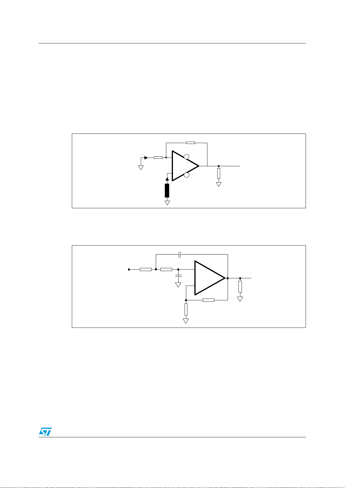
9.1 The bias of an inverting amplifier
A resistance is necessary to achieve good input biasing, such as resistance R, shown in
Figure 66.
The magnitude of this resistance is calculated by assuming the negative and positive input
bias current. The aim is to compensate for the offset bias current, which could affect the
input offset voltage and the output DC component. Assuming Ib-, Ib+, R
volt output, the resistance R is:
R = R
in
// R
fb
Figure 66. Compensation of the input bias current
fb
fb
R
R
Ib-
Ib-
Rin
Rin
Ib+
Ib+
R
R
_
_
+
+
TS616
TS616
Vcc+
Vcc+
Vcc-
Vcc-
Output
Output
Load
Load
, Rfb and a zero
in
9.2 Active filtering
Figure 67. Low-pass active filtering - Sallen-Key
From the resistors Rfb and RG, we can directly calculate the gain of the filter in a classic noninverting amplification configuration:
We assume the following expression as the response of the system:
C1
C1
R
R
1 R2
1 R2
IN
IN
RG
RG
AVg1
Vout
---------------- -
Vin
jω
jω
T
jω
C2
C2
---------------------------------------- -==
12ζ
+
+
_
_
TS616
TS616
910Ω
910Ω
R
fb
--------+==
R
g
jω
-----
ω
OUT
OUT
25Ω
25Ω
fb
fb
R
R
g
2
jω()
----------- -++
2
c
ω
c
29/37
Page 30

Choosing the feedback circuit TS616
The cutoff frequency is not gain-dependent and so becomes:
ω
c
1
------------------------------------ -=
R1R2C1C2
The damping factor is calculated by the following expression:
1
-- -
ζ
ωcC1R1C1R2C2R1C1R1g–++()=
2
The higher the gain the more sensitive the damping factor is. When the gain is higher than
1, it is preferable to use some very stable resistor and capacitor values. In the case of
R1 = R2:
R
fb
--------
–
2C
2C1
R
ζ
-------------------------------- -=
2C1C
g
2
30/37
Page 31

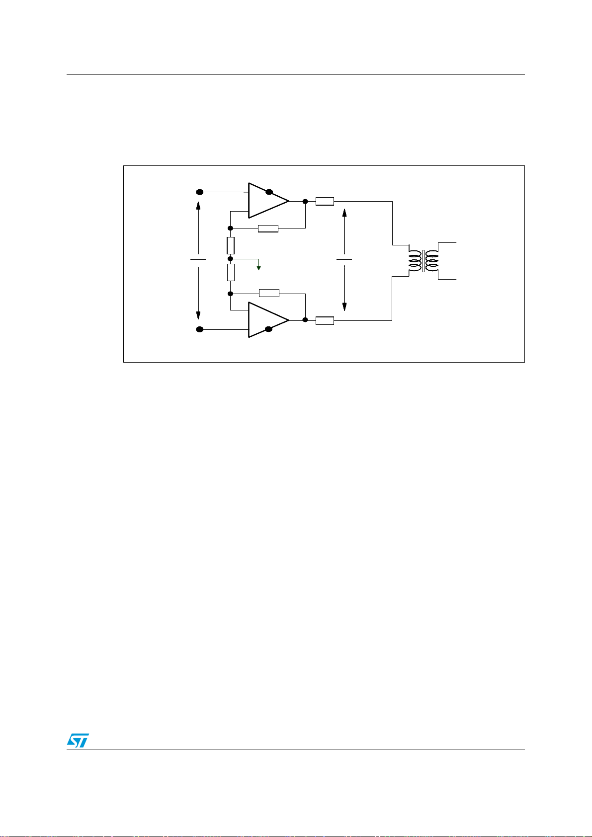
TS616 Increasing the line level using active impedance matching
10 Increasing the line level using active impedance
matching
With passive matching, the output signal amplitude of the driver must be twice the amplitude
on the load. To go beyond this limitation an active matching impedance can be used. With
this technique, it is possible to maintain good impedance matching with an amplitude on the
load higher than half of the output driver amplitude. This concept is shown in Figure 68 for a
differential line.
Figure 68. TS616 as a differential line driver with active impedance matching
1
μ
100n
Vcc+
1k
Vi
1/2
1/2
μ
GND
100n
Vi Vo
10
1k
100n
R1
R1
+
_
Vcc/2
+
_
R2
R3
R5
R4
Vcc+
GND
Vcc+
GND
Rs1
Vo°
Vo°
Rs2
10n
Vo
RL
1:n
Hybrid
&
Transformer
100
Ω
Component calculation
Let us consider the equivalent circuit for a single-ended configuration, as shown in
Figure 69.
Figure 69. Single-ended equivalent circuit
+
+
+
Vi
Vi
½ R1
½ R1
+
_
_
_
_
R2
R2
R3
R3
31/37
Vo°
Vo°
Rs1
Rs1
-1
-1
-1
-1
Vo
Vo
½ RL
½ RL
Page 32

Increasing the line level using active impedance matching TS616
First let’s consider the unloaded system. We can assume that the currents through R1, R2
and R3 are respectively:
2Vi
Vi Vo°–()
-------- -
---------------------------
,
R1
As Vo
° equals Vo without load, the gain in this case becomes:
Vo noload()
G
--------------------------------
R2
Vi
Vi Vo+()
------------------------
and
R3
2R2
1
-----------
R1
----------------------------------- -==
R2
1
------- -–
R3
R2
------- -++
R3
The gain, for the loaded system is given by Equation 6:
Equation 6
2R2
-----------
R1
1
R2
------- -–
R3
R2
------- -++
R3
1
Vo withload()
GL
------------------------------------ -
==
Vi
1
-- -
----------------------------------- -
2
The system shown in Figure 70 is an ideal generator with a synthesized impedance acting
as the internal impedance of the system. From this, the output voltage becomes:
Equation 7
Vo ViG()Ro Iout⋅()–=
where Ro is the synthesized impedance and Iout the output current.
On the other hand Vo can be expressed as:
Equation 8
2R2
-----------
R1
R2
------- -–
R3
R2
------- -++
R3
Rs1Iout
----------------------–=
R2
1
------- -–
R3
⎛⎞
Vi 1
Vo
⎝⎠
-----------------------------------------------
1
By identification of both Equation 7 and Equation 8, the synthesized impedance is, with
Rs1 = Rs2 = Rs:
Equation 9
Ro
Rs
-----------------=
R2
1
------- -–
R3
32/37
Page 33

TS616 Increasing the line level using active impedance matching
Figure 70. Equivalent schematic - Ro is the synthesized impedance
Iout
Ro
Vi.Gi
1/2RL
Let us write Vo°=kVo, where k is the matching factor varying between 1 and 2. If we assume
that the current through R3 is negligible, we can calculate the output resistance, Ro:
Ro
kVoRL
---------------------------- -=
RL 2Rs1+
After choosing the k factor, Rs will be equal to 1/2RL(k-1).
For a good impedance matching we assume that:
Equation 10
1
-- -
Ro
RL=
2
From Equation 9 and Equation 10, we derive:
Equation 11
R2
------- - 1
R3
2Rs
---------- -–=
RL
By fixing an arbitrary value of R2, Equation 11 becomes:
R3
R2
--------------------=
2Rs
1
---------- -–
RL
Finally, the values of R2 and R3 allow us to extract R1 from Equation 6, so that:
Equation 12
R1
---------------------------------------------------------- -=
⎛⎞
21
⎝⎠
R2
------- -–
R3
2R2
GL 1–
R2
------- -–
R3
with GL the required gain.
Table 6. Components calculation for impedance matching implementation
GL (gain for the loaded system)
R1 2R2/[2(1-R2/R3)GL-1-R2/R3]
R2 (= R4) Arbitrarily fixed
R3 (= R5) R2/(1-Rs/0.5RL)
Rs 0.5RL(k-1)
Load viewed by each driver kRL/2
GL is fixed for the application requirements
GL= Vo/Vi= 0.5(1+2R2/R1+R2/R3)/(1-R2/R3)
33/37
Page 34

Package information TS616
11 Package information
In order to meet environmental requirements, ST offers these devices in ECOPACK®
packages. These packages have a Lead-free second level interconnect. The category of
second level interconnect is marked on the package and on the inner box label, in
compliance with JEDEC Standard JESD97. The maximum ratings related to soldering
conditions are also marked on the inner box label. ECOPACK is an ST trademark.
ECOPACK specifications are available at: www.st.com
34/37
Page 35

TS616 Package information
Figure 71. SO-8 exposed pad package mechanical drawing
Table 7. SO-8 exposed pad package mechanical data
Dimensions
Millimeters Inches
Ref.
Min. Typ. Max. Min. Typ. Max.
A 1.350 1.750 0.053 0.069
A1 0.000 0.150 0.001 0.0059
A2 1.100 1.650 0.043 0.065
B 0.330 0.510 0.013 0.020
C 0.190 0.250 0.007 0.010
D 4.800 5.000 0.189 0.197
D1 3.10 0.122
E 3.800 4.000 0.150 0.157
E1 2.41 0.095
e 1.270 0.050
H 5.800 6.200 0.228 0.244
h 0.250 0.500 0.010 0.020
L 0.400 1.270 0.016 0.050
k0d 8d0d 8d
ddd 0.100 0.004
35/37
Page 36

Ordering information TS616
12 Ordering information
Table 8. Order codes
Part number Temperature range Package Packaging Marking
TS616IDW
-40°C to +85°C SO-8
TS616IDWT Tape & reel TS616
13 Revision history
Date Revision Changes
1-Nov-2002 1 First release.
03-Dec-2004 2
24-Oct-2006 3
16-Apr-2007 4 Corrected package error in Table 8: Order codes.
26-Sep-2008 5 Corrected package error in Table 8: Order codes.
Tube TS616
Moved note in Ta bl e 3 to Section 9: Choosing the feedback circuit on
page 28.
Figure 43 in Revision 1, entitled Group Delay, has been removed
because the results presented were not technically meaningful.
Simplified mathematical representations of the intermodulation
product in Section 5: Intermodulation distortion product on page 17.
In Section 6: Printed circuit board layout considerations on page 20,
change from “The copper area can be connected to (-Vcc) available
on pin 4.” to “The copper area
on pin 4.”.
In Section 9.1: The bias of an inverting amplifier on page 29, change
of section title, and correction of referred figure to Figure 66.
Format update.
Corrected package mechanical data for SO-8 exposed pad.
must be connected to -Vcc available
36/37
Page 37

TS616
Please Read Carefully:
Information in this document is provided solely in connection with ST products. STMicroelectronics NV and its subsidiaries (“ST”) reserve the
right to make changes, corrections, modifications or improvements, to this document, and the products and services described herein at any
time, without notice.
All ST products are sold pursuant to ST’s terms and conditions of sale.
Purchasers are solely responsible for the choice, selection and use of the ST products and services described herein, and ST assumes no
liability whatsoever relating to the choice, selection or use of the ST products and services described herein.
No license, express or implied, by estoppel or otherwise, to any intellectual property rights is granted under this document. If any part of this
document refers to any third party products or services it shall not be deemed a license grant by ST for the use of such third party products
or services, or any intellectual property contained therein or considered as a warranty covering the use in any manner whatsoever of such
third party products or services or any intellectual property contained therein.
UNLESS OTHERWISE SET FORTH IN ST’S TERMS AND CONDITIONS OF SALE ST DISCLAIMS ANY EXPRESS OR IMPLIED
WARRANTY WITH RESPECT TO THE USE AND/OR SALE OF ST PRODUCTS INCLUDING WITHOUT LIMITATION IMPLIED
WARRANTIES OF MERCHANTABILITY, FITNESS FOR A PARTICULAR PURPOSE (AND THEIR EQUIVALENTS UNDER THE LAWS
OF ANY JURISDICTION), OR INFRINGEMENT OF ANY PATENT, COPYRIGHT OR OTHER INTELLECTUAL PROPERTY RIGHT.
UNLESS EXPRESSLY APPROVED IN WRITING BY AN AUTHORIZED ST REPRESENTATIVE, ST PRODUCTS ARE NOT
RECOMMENDED, AUTHORIZED OR WARRANTED FOR USE IN MILITARY, AIR CRAFT, SPACE, LIFE SAVING, OR LIFE SUSTAINING
APPLICATIONS, NOR IN PRODUCTS OR SYSTEMS WHERE FAILURE OR MALFUNCTION MAY RESULT IN PERSONAL INJURY,
DEATH, OR SEVERE PROPERTY OR ENVIRONMENTAL DAMAGE. ST PRODUCTS WHICH ARE NOT SPECIFIED AS "AUTOMOTIVE
GRADE" MAY ONLY BE USED IN AUTOMOTIVE APPLICATIONS AT USER’S OWN RISK.
Resale of ST products with provisions different from the statements and/or technical features set forth in this document shall immediately void
any warranty granted by ST for the ST product or service described herein and shall not create or extend in any manner whatsoever, any
liability of ST.
ST and the ST logo are trademarks or registered trademarks of ST in various countries.
Information in this document supersedes and replaces all information previously supplied.
The ST logo is a registered trademark of STMicroelectronics. All other names are the property of their respective owners.
© 2008 STMicroelectronics - All rights reserved
STMicroelectronics group of companies
Australia - Belgium - Brazil - Canada - China - Czech Republic - Finland - France - Germany - Hong Kong - India - Israel - Italy - Japan -
Malaysia - Malta - Morocco - Singapore - Spain - Sweden - Switzerland - United Kingdom - United States of America
www.st.com
37/37
 Loading...