

Features
Control
Voltage
1
2
3
4
5
6
7
14
13
12
11
10
9
8
Discharge
Threshold
Reset
Output
Trigger
GND
Control
Voltage
+V
Discharge
Threshold
Reset
Output
Trigger
S
■ Very low power consumption:
220 µA typ at V
180 µA typ at V
■ High maximum astable frequency 2.7 MHz
■ Pin-to-pin and functionally compatible with
CC
CC
= 5 V
= 3 V
bipolar NE556
■ Wide voltage range: 2 V to 16 V
■ Supply current spikes reduced during output
transitions
■ High input impedance: 10
■ Output compatible with TTL, CMOS and logic
12
Ω
MOS
Description
TS556
Low-power dual CMOS timer
N
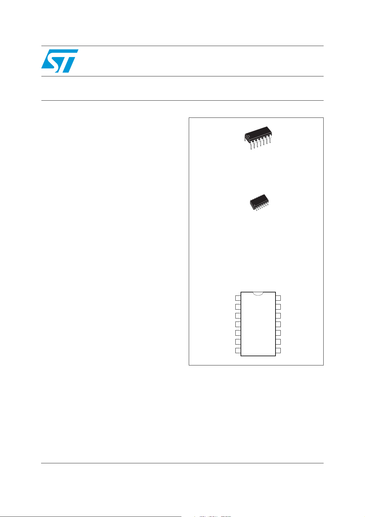
DIP14
(Plastic package)
D
SO14
(Plastic micropackage)
The TS556 is a dual CMOS timer which offers a
very low consumption:
(I
cc(TYP)
I
cc(TYP)
TS556 = 220 µA at VCC=+5V versus
NE556 = 6 mA),
and high frequency:
(f
TS556 = 2.7 MHz versus
(max.)
f
NE556 = 0.1 MHz).
(max.)
In both monostable and astable modes, timing
remains very accurate.
The TS556 provides reduced supply current
spikes during output transitions, which enable the
use of lower decoupling capacitors compared to
those required by bipolar NE556.
Due to the high input impedance (10
12
Ω), timing
capacitors can also be minimized.
Pin connections
(top view)
October 2008 Rev 2 1/19
www.st.com
19
Absolute maximum ratings and operating conditions TS556
1 Absolute maximum ratings and operating conditions
Table 1. Absolute maximum ratings
Symbol Parameter Value Unit
V
I
OUT
CC
Supply voltage +18 V
Output current ± 100 mA
Thermal resistance junction to ambient
R
thja
DIP14
SO14
(2)
(1)
80
105
°C/W
Thermal resistance junction to case
R
thjc
T
j
T
stg
Junction Temperature +150 °C
Storage Temperature Range -65 to +150 °C
Human body model (HBM)
ESD
Charged device model (CDM)
1. Short-circuits can cause excessive heating. These values are typical and specified for a single layer PCB.
2. Short-circuits can cause excessive heating. These values are typical and specified for a four layers PCB.
3. Human body model: a 100 pF capacitor is charged to the specified voltage, then discharged through a
1.5kΩ resistor between two pins of the device. This is done for all couples of connected pin combinations
while the other pins are floating.
4. Machine model: a 200 pF capacitor is charged to the specified voltage, then discharged directly between
two pins of the device with no external series resistor (internal resistor < 5 Ω). This is done for all couples of
connected pin combinations while the other pins remain floating.
5. Charged device model: all pins plus package are charged together to the specified voltage and then
discharged directly to the ground.
Table 2. Operating conditions
DIP14
SO14
(2)
(1)
(4)
(3)
(5)
33
31
1200
200
1000
°C/W
VMachine model (MM)
Symbol Parameter Value Unit
V
I
OUT
CC
Supply voltage 2 to 16 V
Output sink current
Output source current
Operating free air temperature range:
T
oper
TS556C
TS556I
TS556M
2/19
10
50
0 to +70
-40 to +125
-55 to +125
mA
°C
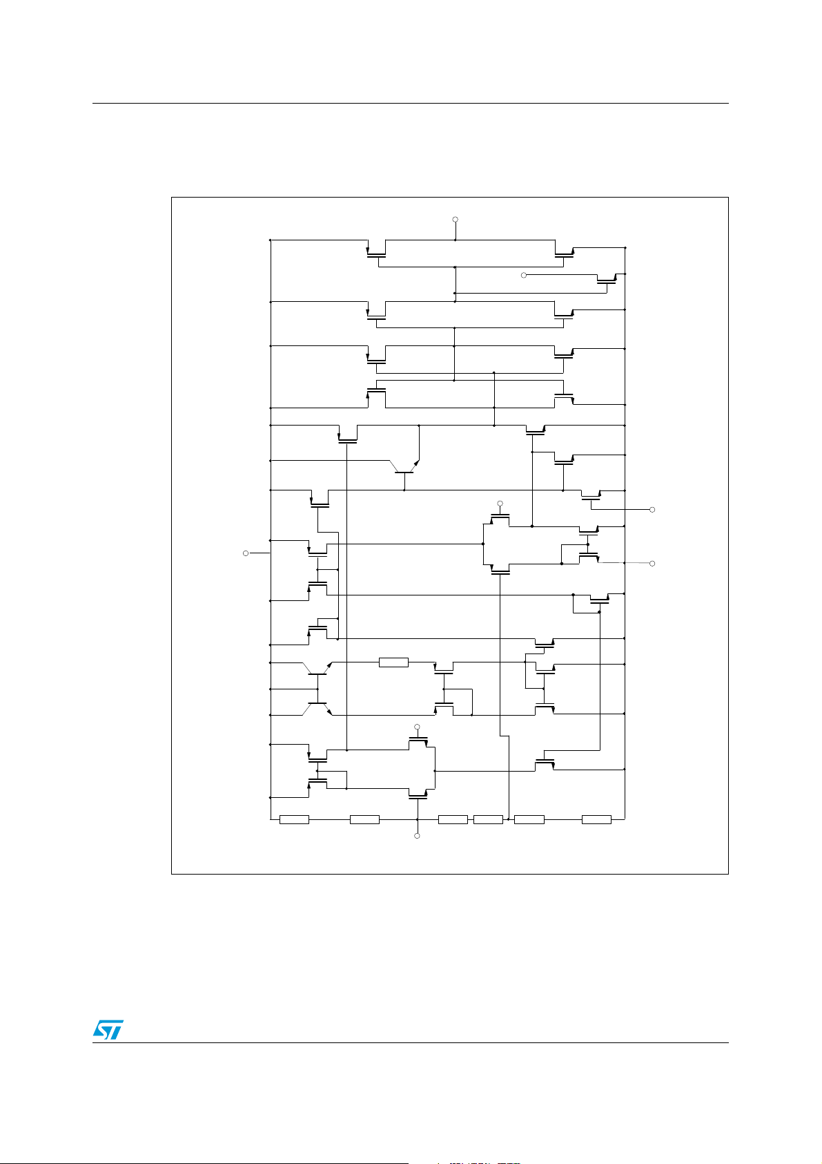
TS556 Schematic diagram
R1
50k
Ω
Τ1
R2
50k
Ω
R3
50k
Ω
R4
50k
Ω
R5
50k
Ω
R6
50k
Ω
Τ2
Τ4
Threshold
Τ5
Τ6
Τ7
Τ14
Τ8
Τ9
Τ15
Τ16
Τ17
Τ18 Τ19
Trigger
Τ24
Τ22
Τ23
Τ28
Τ29
Τ32
Τ35
Τ33
Discharge
Output
Τ10
Τ11
Τ12 Τ13
Τ20
Τ21
Τ26
Τ25
Τ27 Τ30
Τ31
Τ34
GND
RESET
V
CC
R7
2 Schematic diagram
Figure 1. Schematic diagram (1/2 TS556)
3/19
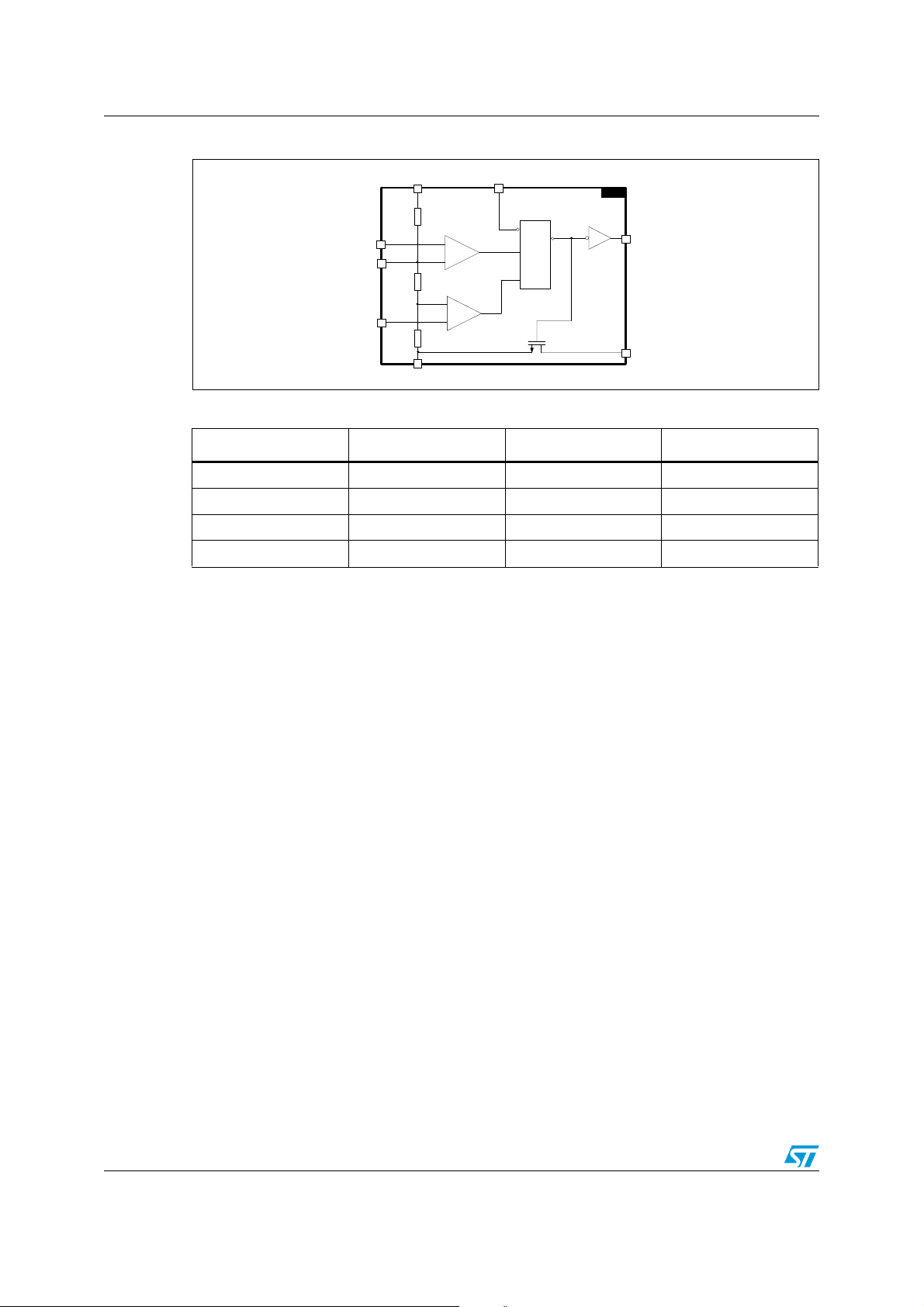
Schematic diagram TS556
Output
Discharge
Ground
Trigger
Control
Voltage
Threshold
V
CC
Reset
R
R
R
B
A
R1
R
S
Q
+
-
+
-
4 / 10
5 / 9
14
2 / 12
3 / 11
6 / 8
7
1 / 13
TS556
Figure 2. Block diagram
Table 3. Functions table
Reset Trigger Threshold Output
Low x x Low
High Low x High
High High High Low
High High Low Previous State
Note: LOW: level voltage ≤ minimum voltage specified
HIGH: level voltage ≥ maximum voltage specified
x: irrelevant.
4/19
TS556 Electrical characteristics
3 Electrical characteristics
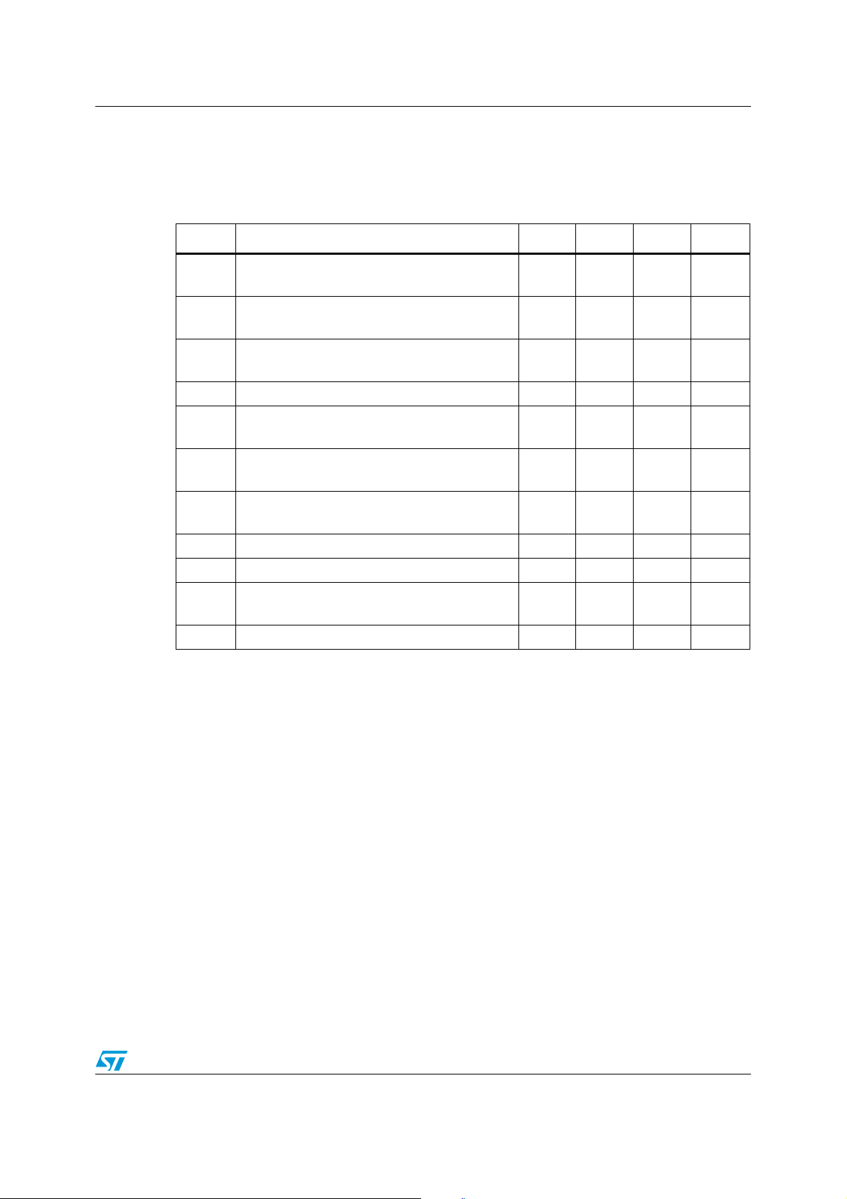
Table 4. Static electrical characteristics
V
= +2 V, T
CC
Symbol Parameter Min. Typ. Max. Unit
= +25 °C, Reset to V
amb
(unless otherwise specified)
CC
I
CC
V
V
I
DIS
V
V
V
TRIG
I
TRIG
I
V
RESET
I
RESET
Supply current (no load, high and low states)
≤ T
T
min.
amb
≤ T
max
Control voltage level
CL
T
min.
≤ T
amb
≤ T
max
Discharge saturation voltage (I
DIS
T
min.
≤ T
amb
≤ T
max
= 1 mA)
dis
1.2
1.1
130 400
1.3 1.4
0.05 0.2
Discharge pin leakage current 1 100 nA
Low level output voltage (I
OL
T
≤ T
min.
amb
High level output voltage (I
OH
T
min.
≤ T
amb
Trigger voltage
≤ T
T
min.
amb
≤ T
≤ T
≤ T
max
max
max
sink
source
= 1 mA)
= -0.3 mA)
1.5
1.5
0.4
0.3
0.1 0.3
1.9
0.67 0.95
Trigger current 10 pA
Threshold current 10 pA
TH
Reset voltage
T
≤ T
amb
≤ T
min.
max
0.4
0.3
1.1 1.5
Reset current 10 pA
400
1.5
0.25
0.35
1.05
2.0
µA
V
V
V
V
V
V
5/19
Electrical characteristics TS556
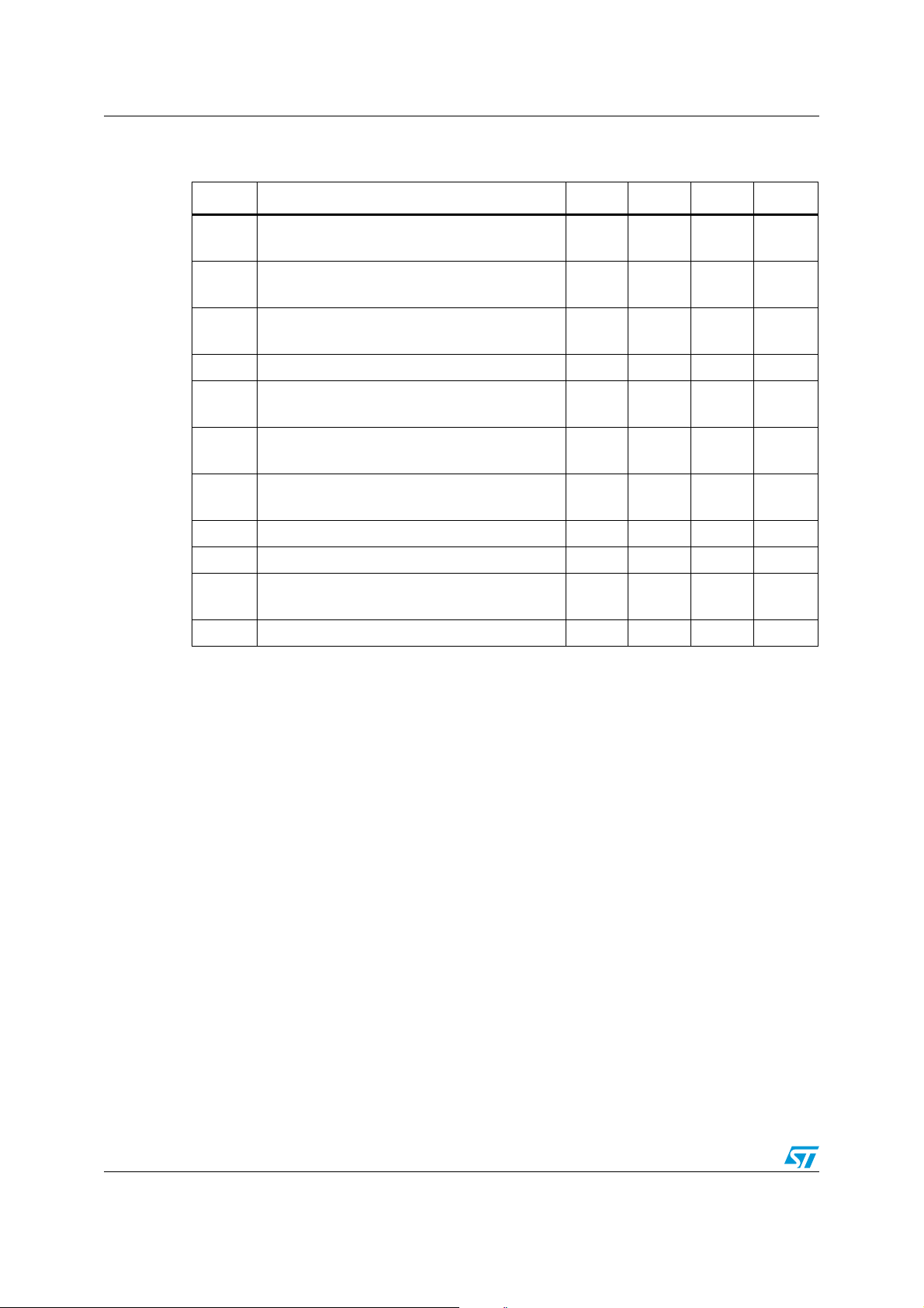
Table 5. Static electrical characteristics
V
= +3 V, T
CC
Symbol Parameter Min. Typ. Max. Unit
= +25 °C, Reset to VCC (unless otherwise specified)
amb
I
CC
V
V
I
DIS
V
V
V
TRIG
I
TRIG
I
V
RESET
I
RESET
Supply current (no load, high and low states)
T
≤ T
amb
≤ T
max
min
Control voltage level
CL
T
≤ T
amb
≤ T
max
min
Discharge saturation voltage (I
DIS
T
≤ T
amb
≤ T
max
min
= 1 mA)
dis
1.8
1.7
180 460
22.2
0.05 0.2
Discharge pin leakage current 1 100 nA
Low level output voltage (I
OL
T
min.
≤ T
amb
High level output voltage (I
OH
T
min.
≤ T
amb
Trigger voltage
≤ T
T
min.
amb
≤ T
≤ T
≤ T
max
max
max
sink
source
= 1 mA)
= -0.3 mA)
2.5
2.5
0.9
0.8
0.1 0.3
2.9
11.1
Trigger current 10 pA
Threshold current 10 pA
TH
Reset voltage
≤ T
T
min.
amb
≤ T
max
0.4
0.3
1.1 1.5
Reset current 10 pA
460
2.3
0.25
0.35
1.2
2.0
µA
V
V
V
V
V
V
6/19
 Loading...