

Precision low noise dual operational amplifier
Features
■ Large output voltage swing
+14.3V/-14.6 V
■ Low input offset voltage 850 μV max.
■ Low voltage noise: 4.5 nV/√Hz
■ High gain bandwidth product: 15 MHz
■ High slew rate: 7 V/μs
■ Low distortion: 0.002 %
■ ESD internal protection 2 kV
■ Excellent frequency stability
■ Macromodel included in this specification
Description
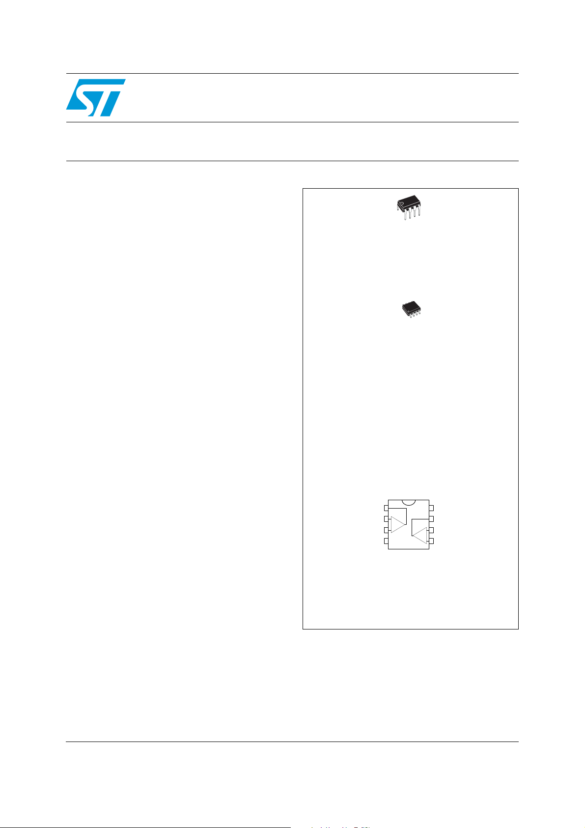
TS522
N
DIP8
(Plastic Package)
D
SO8
(Plastic Micropackage)
The TS522 is a monolithic dual operational
amplifier mainly dedicated to audio applications.
The TS522 offers a very low input offset voltage
as well as low voltage noise (4.5 nV/√Hz) and
high dynamic performances (15 MHz gain
bandwidth product, 7 V/μs slew rate).
The output stage allows a large output voltage
swing and symmetrical source and sink currents.
Output 1
Inverting input 1
Non-inverting input 1
V
Pin connections
top view
+
-
+
V
8
CC
Output 2
7
6
Inverting input 2
Non-inverting input 2
1
2
-
+
3
-
45
CC
October 2008 Rev 2 1/13
www.st.com
13
Absolute maximum ratings and operating conditions TS522
1 Absolute maximum ratings and operating conditions
Table 1. Absolute maximum ratings
Symbol Parameter Value Unit
V
V
T
R
R
ESD
1. Either or both input voltages must not exceed the magnitude of V
2. Power dissipation must be considered to ensure maximum junction temperature (Tj) is not exceeded.
3. Short-circuits can cause excessive heating and destructive dissipation.
4. R
5. Human body model: a 100 pF capacitor is charged to the specified voltage, then discharged through a
1.5 kΩ resistor between two pins of the device. This is done for all couples of connected pin combinations
while the other pins are floating.
6. Machine model: a 200 pF capacitor is charged to the specified voltage, then discharged directly between
two pins of the device with no external series resistor (internal resistor < 5 Ω). This is done for all couples of
connected pin combinations while the other pins are floating.
7. Charged device model: all pins and the package are charged together to the specified voltage and then
discharged directly to the ground through only one pin. This is done for all pins.
Table 2. Operating conditions
Supply voltage ±18 to 36 V
CC
(6)
(1)
(5)
(2)
(7)
(3) (4)
(3) (4)
CC
+
or V
CC
±30 V
±15 V
Infinite
125
85
40
41
2kV
200 V
1.5 kV
-
Differential input voltage
id
V
i
Input voltage
(1)
Output short-circuit duration
T
Maximum junction temperature + 150 °C
j
Storage temperature range -65 to +150 °C
stg
Thermal resistance junction to ambient
thja
SO-8
DIP8
Thermal resistance junction to case
thjc
SO-8
DIP8
HBM: human body model
MM: machine model
CDM: charged device model
are typical values.
th
°C/W
°C/W
Symbol Parameter Value Unit
V
T
Supply voltage ±2.5 to ±15 V
CC
Operating free-air temperature range -40 to 125 °C
oper
2/13
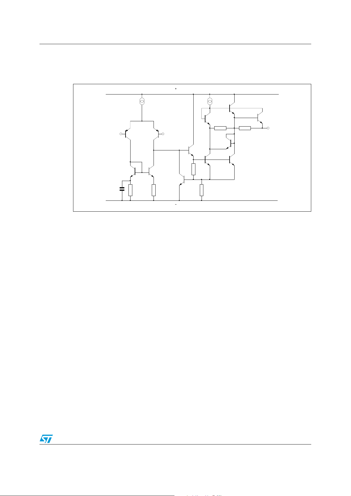
TS522 Schematic diagram
2 Schematic diagram
Figure 1. Typical schematic diagram (1/2 TS522)
V
CC
Inverting
Input
Non-inverting
Input
V
CC
Output
3/13
Electrical characteristics TS522
3 Electrical characteristics
Table 3. VCC+ = 15 V, VCC- = -15 V, T
(unless otherwise specified)
Symbol Parameter Min. Typ. Max. Unit
amb
= 25° C
V
ΔV
Iio
I
ib
Vicm
A
±V
Input offset voltage (Vo = 0V, Vic = 0V)
io
io
amb
T
≤ T
amb
≤ T
max
min
Input offset voltage drift
Vic = 0V, Vo = 0V, T
min
Input offset current (V
T
= +25°C
amb
≤ T
amb
≤ T
max
T
min
≤ T
≤ T
amb
= 0V, Vo = 0V)
ic
max
= +25°C
T
Input bias current (Vic = 0V, Vo = 0V)
= +25°C
T
amb
T
≤ T
≤ T
min
amb
max
Common mode input voltage range
(ΔV
= 5mV, Vo = 0V) ±13 ±14 V
io
Large signal voltage gain (RL = 2kΩ, Vo = ±10V)
= +25°C
vd
T
T
amb
min
≤ T
amb
≤ T
max
Output voltage swing (Vid = ±1V)
RL = 600Ω
= 600Ω
R
L
opp
RL = 2.0kΩ
= 2.0kΩ
R
L
90
85
13.2
0.85
1.7
2
10 150
175
250 750
800
100
12.2
-12.7
14
-14.2
-13.2
mV
μV/°C
nA
nA
dB
V
RL = 10kΩ
= 10kΩ
R
L
CMR Common mode rejection ratio (V
SVR
Supply voltage rejection ratio
+
Vcc
/Vcc- = +15V/-15V to +5V/-5V 80 105
Output short circuit current
= ±1V, Output to ground)
(V
I
o
id
Source
Sink
Supply current (Vo = 0V, all amplifiers)
I
cc
SR
GBP
= +25°C
T
amb
T
≤ T
≤ T
min
amb
max
Slew rate
= -10V to +10V, RL = 2kΩ, CL = 100pF, AV = +1) 5 7 V/μs
(V
i
Gain bandwidth product
(f = 100kHz, R
= 2kΩ, CL = 100pF) 10 15 MHz
L
B Unity gain bandwidth (open loop) 9 MHz
4/13
13.5
= ±13V) 80 100 dB
ic
15
20
14.3
-14.6
29
37
-14
45
5.5
dB
mA
mA
 Loading...