TS4999
Filter-free stereo 2.8 W class D audio power amplifier
with selectable 3D sound effects
Features
■ Operates from V
■ Dedicated standby mode active low/channel
■ Output power per channel: 2.8 W at 5 V into
4 Ω with 10% THD+N or 0.7 W at 3.6 V into 8 Ω
with 1% THD+N max.
■ Selectable 3D sound effect
■ Four gain setting steps: 3.5, 6, 9.5 and 12 dB
■ Low current consumption
■ PSSR: 63 dB typical at 217 Hz.
■ Fast start up phase: 7.8 ms
■ Short-circuit and thermal shutdown protection
■ Flip chip 18-bump lead-free package
= 2.4 to 5.5 V
CC
Applications
■ Cellular phones
■ PDAs
■ Notebook PCs
Flip chip 18-bump package
Pin connections (top view)
LOUT-
LOUT-
LOUT+
LOUT+
STDBYL
STDBYL
LPVCC
LPVCC
AGND
AGND
LIN- RIN-
LIN- RIN-
PGND
PGND
G1
G1
G0
G0
RPVCC
RPVCC
AVCC
AVCC
ROUT-
ROUT-
ROUT+
ROUT+
STDBYR
STDBYR
RIN+3D
Description
LIN+
LIN+
RIN+3D
The TS4999 is a stereo fully-differential class D
power amplifier. It can drive up to 1.35 W into a
8 Ω load at 5 V per channel. The device has four
different gain settings utilizing two discrete pins,
G0 and G1.
Pop and click reduction circuitry provides low
on/off switch noise while allowing the device to
start within 8 ms. 3D enhancement effects are
selected through one digital input pin that allows
more amazing stereo audio sound.
Two standby pins (active low) allow each channel
to be switched off separately.
The TS4999 is available in a flip chip, 18-bump,
lead-free package.
December 2008 Rev 1 1/36
www.st.com
36

Contents TS4999
Contents
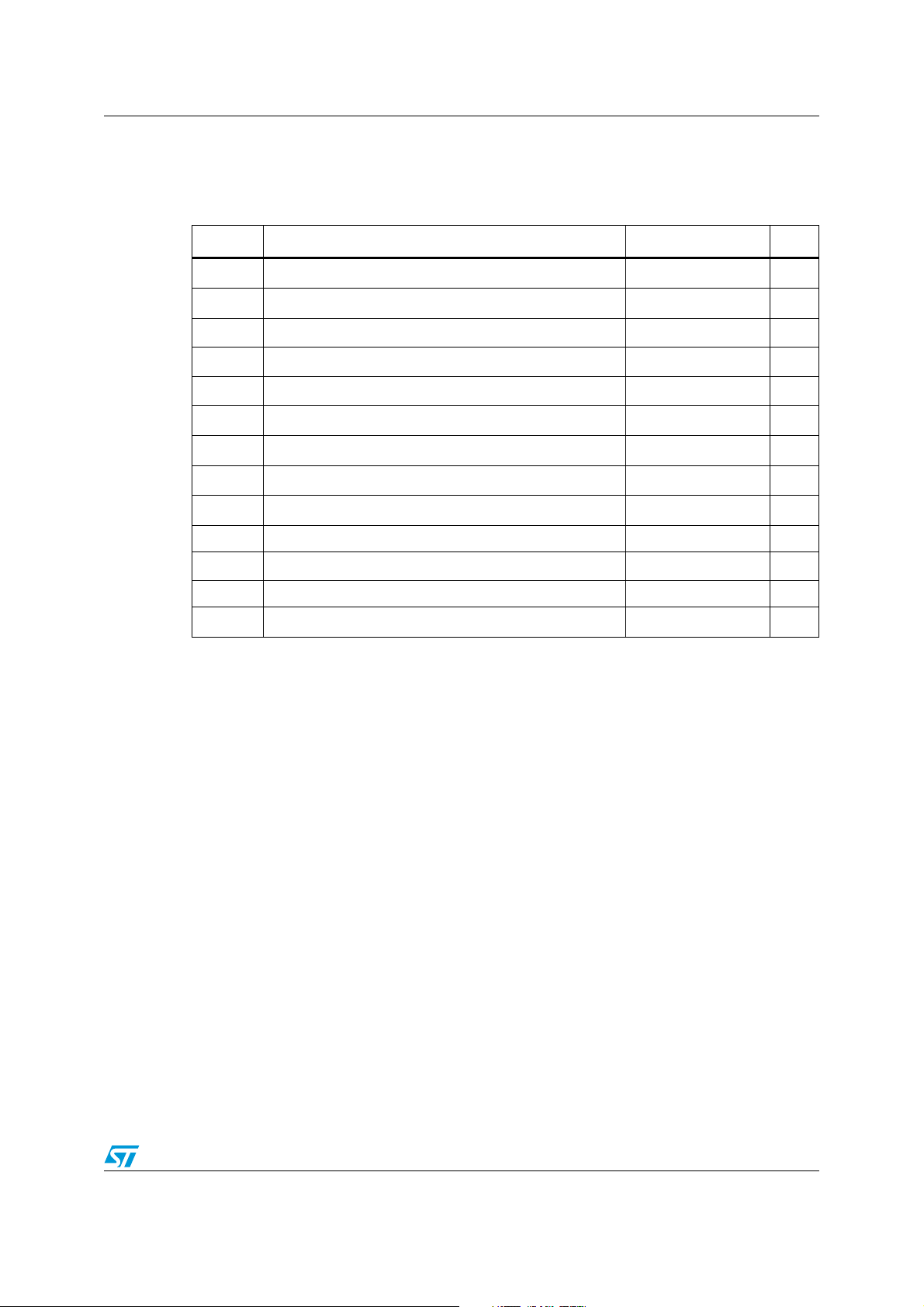
1 Absolute maximum ratings . . . . . . . . . . . . . . . . . . . . . . . . . . . . . . . . . . . 3
2 Application information . . . . . . . . . . . . . . . . . . . . . . . . . . . . . . . . . . . . . . 5
3 Electrical characteristics . . . . . . . . . . . . . . . . . . . . . . . . . . . . . . . . . . . . . 7
3.1 Electrical characteristic curves . . . . . . . . . . . . . . . . . . . . . . . . . . . . . . . . . 13
4 Application information . . . . . . . . . . . . . . . . . . . . . . . . . . . . . . . . . . . . . 24
4.1 Differential configuration principle . . . . . . . . . . . . . . . . . . . . . . . . . . . . . . 24
4.2 Gain settings . . . . . . . . . . . . . . . . . . . . . . . . . . . . . . . . . . . . . . . . . . . . . . 24
4.3 3D effect enhancement . . . . . . . . . . . . . . . . . . . . . . . . . . . . . . . . . . . . . . 24
4.4 Low frequency response . . . . . . . . . . . . . . . . . . . . . . . . . . . . . . . . . . . . . 25
4.5 Circuit decoupling . . . . . . . . . . . . . . . . . . . . . . . . . . . . . . . . . . . . . . . . . . . 26
4.6 Wakeup (t
4.7 Consumption in shutdown mode . . . . . . . . . . . . . . . . . . . . . . . . . . . . . . . 28
4.8 Single-ended input configuration . . . . . . . . . . . . . . . . . . . . . . . . . . . . . . . 28
4.9 Output filter considerations . . . . . . . . . . . . . . . . . . . . . . . . . . . . . . . . . . . . 29
4.10 Short-circuit protection . . . . . . . . . . . . . . . . . . . . . . . . . . . . . . . . . . . . . . . 30
4.11 Thermal shutdown . . . . . . . . . . . . . . . . . . . . . . . . . . . . . . . . . . . . . . . . . . 30
) and shutdown (t
WU
) times . . . . . . . . . . . . . . . . . . . . . . . 26
STBY
5 Package mechanical data . . . . . . . . . . . . . . . . . . . . . . . . . . . . . . . . . . . . 31
5.1 Flip chip package . . . . . . . . . . . . . . . . . . . . . . . . . . . . . . . . . . . . . . . . . . . 31
5.2 Tape and reel package . . . . . . . . . . . . . . . . . . . . . . . . . . . . . . . . . . . . . . . 33
6 Ordering information . . . . . . . . . . . . . . . . . . . . . . . . . . . . . . . . . . . . . . . 34
7 Revision history . . . . . . . . . . . . . . . . . . . . . . . . . . . . . . . . . . . . . . . . . . . 35
2/36

TS4999 Absolute maximum ratings
1 Absolute maximum ratings
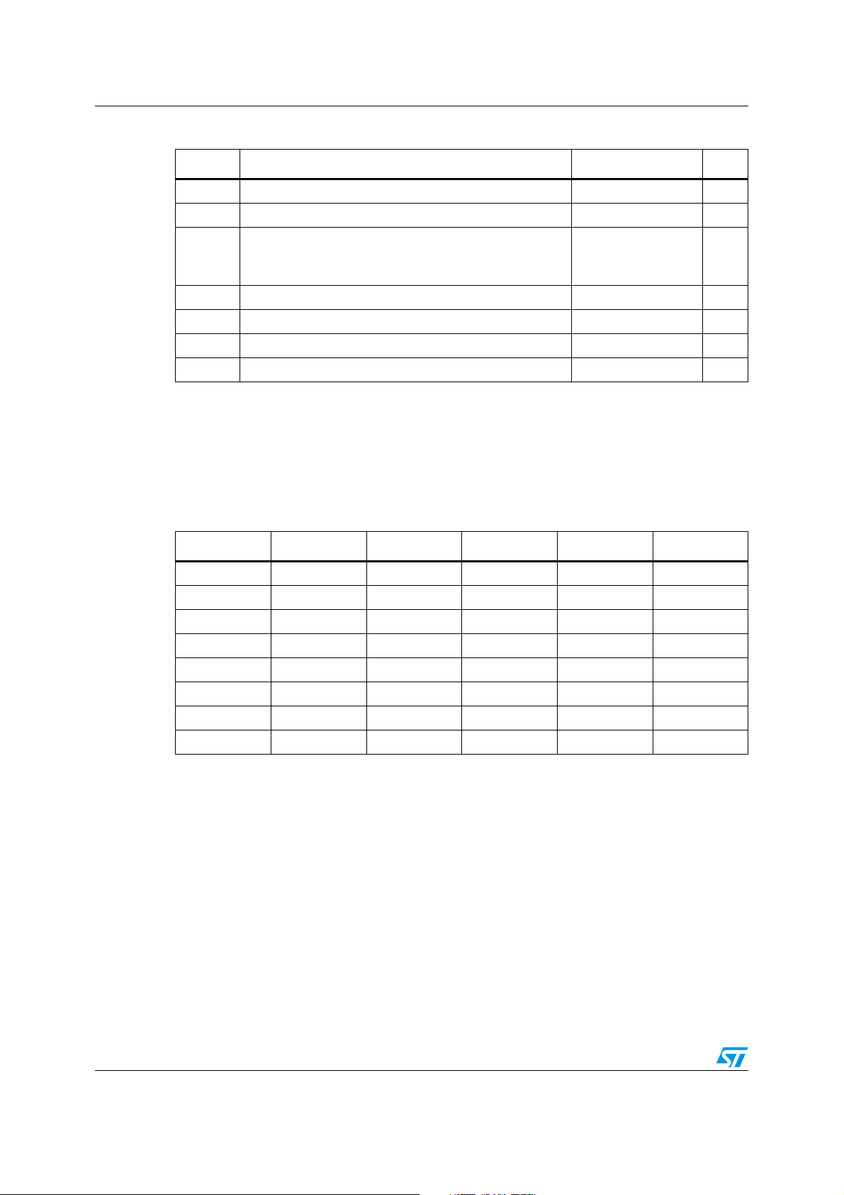
Table 1. Key parameters and their absolute maximum ratings
Symbol Parameter Value Unit
(2)
(1)
(6)
(5)
(3)
6V
GND to V
CC
200 °C/W
Internally Limited
2kV
200 V
(4)
V
T
T
R
V
oper
Supply voltage
CC
Input voltage
in
Operating free air temperature range -40 to + 85 °C
Storage temperature -65 to +150 °C
stg
T
Maximum junction temperature 150 °C
j
Thermal resistance junction to ambient
thja
Pd Power dissipation
ESD
ESD
HBM: human body model
MM: machine model
Latch-up Latch-up immunity 200 mA
V
STBY
Standby pin voltage maximum voltage
GND to V
CC
Lead temperature (soldering, 10 secs) 260 °C
Output short-circuit protection
1. All voltages values are measured with respect to the ground pin.
2. The magnitude of input signal must never exceed VCC + 0.3 V / GND - 0.3 V
3. Device is protected in case of over temperature by a thermal shutdown active at 150° C.
4. Exceeding the power derating curves during a long period, involves abnormal operating condition.
5. Human body model: 100 pF discharged through a 1.5 kΩ resistor between two pins of the device, done for
all couples of pin combinations with other pins floating.
6. Machine model: a 200 pF capacitor is charged to the specified voltage, then discharged directly between
two pins of the device with no external series resistor (internal resistor < 5 Ω), done for all couples of pin
combinations with other pins floating.
7. Implemented short-circuit protection protects the amplifier against damage by short-circuit between
positive and negative outputs of each channel and between outputs and ground.
(7)
V
V
3/36

Absolute maximum ratings TS4999
Table 2. Operating conditions
Symbol Parameter Value Unit
V
V
Supply voltage
CC
Input voltage range GND to V
in
Standby voltage input
VSTBY
Device ON
Device OFF
RL Load resistor
VIH G0, G1, 3D, High Level Input Voltage
VIL G0, G1, 3D, Low Level Input Voltage GND
R
1. For VCC from 2.4 to 2.5 V, the operating temperature range is reduced to 0° C ≤ T
2. Without any signal on V
3. Minimum current consumption is obtained when V
4. Between G0, G1, 3D pins and GND, there is an internal 300 kΩ (+/-20 %) pull-down resistor. When pins
are floating, the gain is 3.5 dB and 3D effect is off. In full standby (left and right channels OFF), these
resistors are disconnected (HiZ input).
5. With a 4-layer PCB.
Table 3. 3D effect pin and STANDBY pins setting truth table
Thermal Resistance Junction to Ambient
thja
(1)
(2)
(4)
(5)
, the device will be in standby (internal 300 kΩ (+/-20 %) pull down resistor)
STBY
= GND
STBY
2.4 to 5.5 V
1.4 ≤ V
GND ≤ V
≤ VCC
STBY
≤ 0.4
STBY
≥4 Ω
1.4 ≤ VIH ≤ VCC V
≤ VIL ≤ 0.4 V
90 °C/W
≤70° C
amb
CC
V
(3)
3D STBYL STBYR 3D Effect Left channel Right channel
0 0 0 X STDBY STDBY
001OFFSTDBYON
010OFFONSTDBY
011OFFONON
1 0 0 X STDBY STDBY
1 0 1 N/A N/A N/A
1 1 0 N/A N/A N/A
1 1 1 ON ON ON
Note: When the 3D effect is switched on, both channels must be in operation or in shutdown mode
at the same time.
4/36

TS4999 Application information
2 Application information
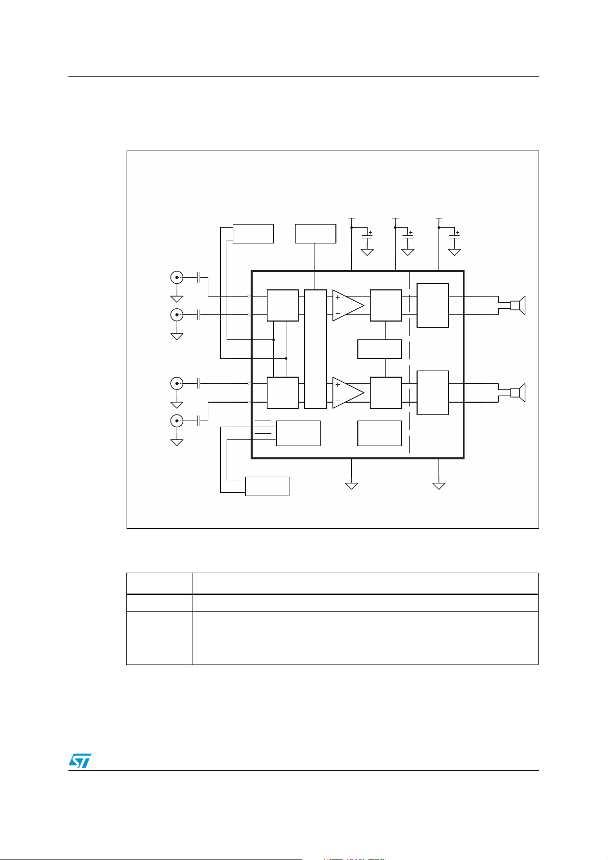
Figure 1. Typical application schematic
Differential
Left Input
Left IN+
Left IN-
Differential
Right Input
Right IN+
Right IN-
Cs
VCC VCC
0.1uF
Gain
3D Effect
Control
C13D
D4
AVCC
Oscillator
Gain Select
Control
TS49 99
Cin
Cin
Lin+
A1
Select
Lin-
B2
G0
C3
C5
G1
RPVCC
PWM
CsR
1uF
D6
VCC
LPVCC
H
Bridge
CsL
1uF
B6
Lout+
A5
A7
Lout-
Left speaker
3D EFFECT
E1
Rin+
Cin
Cin
D2
A3
E3
Gain
Select
Rin-
STBYL
STBYR
Standby Control
Standby
Control
PWM
Protection
Circuit
B4
H
Bridge
PGNDAGND
C7
Rout+
Rout-
E5
E7
Right speaker
Note: See Section 4.9: Output filter considerations on page 29.
Table 4. External component description
Components Functional description
, CSL, C
C
S
C
in
Supply capacitor that provides power supply filtering.
SR
Input coupling capacitors that block the DC voltage at the amplifier input terminal.
The capacitors also form a high pass filter with Z
(Fcl = 1 / (2 x π x Zin x Cin)). Note that the value of Z
These coupling capacitors are mandatory.
5/36
in
changes with each gain setting.
in

Application information TS4999
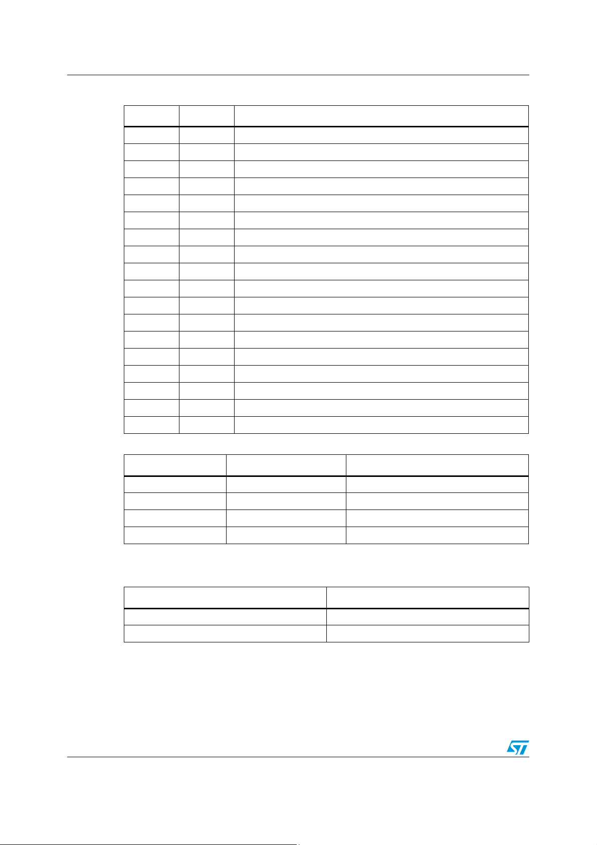
Table 5. Pin description
Bump Name Function
A1 LIN+ Left channel positive differential input
B2 LIN- Left channel negative differential input
C1 3D 3D effect digital input pin
E1 RIN+ Right channel positive differential input
D2 RIN- Right channel negative differential input
A3 STBYL Standby input pin (active low) for left channel output
C3 G0 Gain select input pin (LSB)
E3 STBYR Standby input pin (active low) for right channel output
B4 AGND Analog ground
D4 AVCC Analog supply voltage
A5 LOUT+ Left channel negative output
C5 G1 Gain select input pin (MSB)
E5 ROUT+ Right channel positive output
B6 LPVCC Left channel power supply voltage
D6 RPVCC Right channel power supply voltage
A7 LOUT- Left channel negative output
C7 PGND Power ground
E7 ROUT- Right channel negative output
Table 6. Truth table for output gain settings
G1 G0 Gain value (dB)
0 0 3.5
01 6
10 9.5
11 12
Note: See Table 3 on page 4.
Table 7. Truth table for 3D effects pin settings
3D 3D effect
0OFF
1ON
6/36

TS4999 Electrical characteristics
3 Electrical characteristics
Table 8. VCC = +5 V, GND = 0 V, T
.
= 25° C (unless otherwise specified)
amb
Symbol Parameter Conditions Min. Typ. Max. Unit
I
I
STANDBY
Voo Output offset voltage
Supply current No input signal, no load, both channels 5 7 mA
CC
Standby current No input signal, Vstdby = GND 1 2 μA
Floating inputs, RL = 8Ω, G = 3.5dB,
3D effect off
20 mV
THD = 1% max, F = 1kHz, RL = 4Ω 2.25
Po Output power
THD+N
Total harmonic distortion +
noise
Efficiency Efficiency per channel
PSRR
Power supply rejection ratio
with inputs grounded
Crosstalk Channel separation
THD = 1% max, F = 1kHz, R
THD = 10% max, F = 1kHz, R
THD = 10% max, F = 1kHz, R
Po = 0.9W/Ch, G = 6dB, F=1kHz,
= 8Ω
R
L
Po = 2.3 W
Po = 1.4 W
= 1µF
C
in
, RL = 4Ω +15µH 82
RMS
, RL = 8Ω + 15µH 89
RMS
(1)
,3D effects off
F = 217Hz, RL = 8Ω, gain = 6dB,
Vripple = 200mVpp, Inputs grounded
F = 1kHz, R
= 8Ω,
L
3D effects off
= 8Ω 1.35
L
= 4Ω 2.8 W
L
= 8Ω 1.7 W
L
0.2 %
65 dB
100 dB
W
%
CMRR
Common mode rejection
ratio
Gain Gain value with no load
Single-ended input
IN
impedance referred to GND
Pulse width modulator
base frequency
F
Z
PWM
SNR Signal to noise ratio
t
WU
Wake-up time Total wake-up time
C
=1µF, F = 217Hz, RL = 8Ω, gain = 6dB,
in
ΔVIC = 200mVpp, 3D effects OFF
57 dB
G1 = G0 = "0" 3 3.5 4
G1 = "0" & G0 = "1" 5.5 6 6.5
dB
G1 = "1" & G0 = "0" 9 9.5 10
G1 = G0 = "1" 11.5 12 12.5
G1 = G0 = 3D = "0" or
G1 = "0" & G0 = "1" & 3D = "0" or
24 30 36 kΩ
G1 = "1" & G0 = "0" & 3D = "0"
G1 = "1" & G0 = "1" & 3D = "0" 12 15 18 kΩ
G1 = G0 = "0" & 3D = "1" or
G1 = "0" & G0 = "1" & 3D = "1" or
13.5 17.1 20.5 kΩ
G1 = "1" & G0 = "0" & 3D = "1"
G1 = "1" & G0 = "1" & G3D = "1" 6.5 8.6 10.5
190 280 370 kHz
= 1.3W, A-weighting, RL = 8Ω,
P
o
Gain = 6dB, 3D effects OFF
(2)
99 dB
9 13 16.5 ms
7/36

Electrical characteristics TS4999
Table 8. VCC = +5 V, GND = 0 V, T
= 25° C (unless otherwise specified) (continued)
amb
Symbol Parameter Conditions Min. Typ. Max. Unit
t
STBY
Standby time Standby time
(2)
11 15.8 20 ms
F = 20Hz to 20kHz, A-weighted,
Gain = 3.5dB
Filterless, 3D effect off, R
Filterless, 3D effect on, RL = 4Ω
V
Output voltage noise
N
With LC output filter, 3D effect off, R
With LC output filter, 3D effect on, RL = 4Ω
Filterless, 3D effect off, RL = 8Ω
Filterless, 3D effect on, R
With LC output filter, 3D effect off, RL = 8Ω
With LC output filter, 3D effect on, RL = 8Ω
1. Dynamic measurements - 20*log(rms(Vout)/rms(Vripple)). Vripple is the super-imposed sinus signal to VCC at f = 217 Hz
with fixed Cin cap (input decoupling capacitor).
2. See Section 4.6: Wakeup (t
) and shutdown (t
WU
) times on page 26.
STBY
= 4Ω
L
= 8Ω
L
= 4Ω
L
31
50
30
48
32
51
31
50
μV
RMS
8/36

TS4999 Electrical characteristics
Table 9. VCC = +3.6V, GND = 0V, T
.
= 25°C (unless otherwise specified)
amb
Symbol Parameter Conditions Min. Typ. Max. Unit
I
I
STANDBY
Voo Output offset voltage
Po Output power
THD+N
Efficiency Efficiency per channel
PSRR
Crosstalk Channel separation
CMRR
Supply current No input signal, no load, both channels 3.5 5.5 mA
CC
Standby current No input signal, Vstdby = GND 1 2 μA
Floating inputs, RL = 8Ω, G = 3.5dB,
3D effect off
= 4Ω 1.15
L
= 8Ω 0.7
L
= 4Ω 1.45 W
L
= 8Ω 0.86 W
L
0.15 %
64 dB
102 dB
55 dB
Total harmonic distortion +
noise
Power supply rejection ratio
with inputs grounded
Common mode rejection
ratio
THD = 1% max, F = 1kHz, R
THD = 1% max, F = 1kHz, R
THD = 10% max, F = 1kHz, R
THD = 10% max, F = 1kHz, R
Po = 0.45W/Ch, G = 6dB, F=1kHz,
= 8Ω
R
L
Po = 1.15 W
Po = 0.7 W
= 1µF
C
in
F = 217Hz, R
, RL = 4Ω +15µH 82
RMS
, RL = 8Ω + 15µH 89
RMS
(1)
,3D effects off
= 8Ω, gain = 6dB,
L
Vripple = 200mVpp, inputs grounded
F = 1kHz, R
= 8Ω,
L
3D effects off
=1µF, F = 217Hz, RL = 8Ω, gain = 6dB,
C
in
ΔVIC = 200mVpp, 3D effects off
20 mV
W
%
Gain Gain value with no load
Single-ended input
IN
impedance referred to GND
Pulse width modulator
base frequency
F
Z
PWM
SNR Signal to noise ratio
t
WU
Wake-up time Total wake-up time
G1 = G0 = "0" 3 3.5 4
G1 = "0" & G0 = "1" 5.5 6 6.5
dB
G1 = "1" & G0 = "0" 9 9.5 10
G1 = G0 = "1" 11.5 12 12.5
G1 = G0 = 3D = "0" or
G1 = "0" & G0 = "1" & 3D = "0" or
24 30 36 kΩ
G1 = "1" & G0 = "0" & 3D = "0"
G1 = "1" & G0 = "1" & 3D = "0" 12 15 18 kΩ
G1 = G0 = "0" & 3D = "1" or
G1 = "0" & G0 = "1" & 3D = "1" or
13.5 17.1 20.5 kΩ
G1 = "1" & G0 = "0" & 3D = "1"
G1 = "1" & G0 = "1" & G3D = "1" 6.5 8.6 10.5 kΩ
190 280 370 kHz
P
= 0.67W, A-weighting, RL = 8Ω,
o
Gain = 6dB, 3D effects OFF
(2)
97 dB
7.5 11.3 15 ms
9/36

Electrical characteristics TS4999
Table 9. VCC = +3.6V, GND = 0V, T
= 25°C (unless otherwise specified) (continued)
amb
Symbol Parameter Conditions Min. Typ. Max. Unit
t
STBY
Standby time Standby time
(2)
10 13.8 18 ms
F = 20Hz to 20kHz, A-Weighted,
Gain = 3.5dB
Filterless, 3D effect off, R
Filterless, 3D effect on, RL = 4Ω
V
Output voltage noise
N
With LC output filter, 3D effect off, R
With LC output filter, 3D effect on, RL = 4Ω
Filterless, 3D effect off, RL = 8Ω
Filterless, 3D effect on, R
With LC output filter, 3D effect off, RL = 8Ω
With LC output filter, 3D effect on, RL = 8Ω
1. Dynamic measurements - 20*log(rms(Vout)/rms(Vripple)). Vripple is the super-imposed sinus signal to VCC at f = 217 Hz
with fixed Cin cap (input decoupling capacitor).
2. See Section 4.6: Wakeup (t
) and shutdown (t
WU
) times on page 26.
STBY
= 4Ω
L
= 8Ω
L
= 4Ω
L
29
49
28
48
29
50
29
50
μV
RMS
10/36

TS4999 Electrical characteristics
Table 10. VCC = +2.5 V, GND = 0V, T
= 25° C (unless otherwise specified)
amb
Symbol Parameter Conditions Min. Typ. Max. Unit
I
I
STANDBY
Voo Output offset voltage
Po Output power
THD+N
Efficiency Efficiency per channel
PSRR
Crosstalk Channel separation
CMRR
Supply current No input signal, no load, both channels 2.8 4 mA
CC
Standby current No input signal, Vstdby = GND 1 2 μA
Floating inputs, RL = 8Ω, G = 3.5dB,
3D effect off
= 4Ω 0.53
L
= 8Ω 0.33
L
= 4Ω 0.67 W
L
= 8Ω 0.4 W
L
0.07 %
63 dB
104 dB
55 dB
Total harmonic distortion +
noise
Power supply rejection ratio
with inputs grounded
Common mode rejection
ratio
THD = 1% max, F = 1kHz, R
THD = 1% max, F = 1kHz, R
THD = 10% max, F = 1kHz, R
THD = 10% max, F = 1kHz, R
Po = 0.2W/Ch, G = 6dB, F=1kHz,
= 8Ω
R
L
Po = 0.52 W
Po = 0.33 W
= 1µF
C
in
F = 217Hz, R
, RL = 4Ω +15µH 81
RMS
, RL = 8Ω + 15µH 88
RMS
(1)
,3D effects off
= 8Ω, gain = 6dB,
L
Vripple = 200mVpp, Inputs grounded
F = 1kHz, R
= 8Ω,
L
3D effects off
=1µF, F = 217Hz, RL = 8Ω, gain = 6dB,
C
in
ΔVIC = 200mVpp, 3D effects off
20 mV
W
%
Gain Gain value with no load
Single-ended input
IN
impedance referred to GND
Pulse width modulator
base frequency
F
Z
PWM
SNR Signal to noise ratio
t
WU
Wake-up time Total wake-up time
G1 = G0 = "0" 3 3.5 4
G1 = "0" & G0 = "1" 5.5 6 6.5
dB
G1 = "1" & G0 = "0" 9 9.5 10
G1 = G0 = "1" 11.5 12 12.5
G1 = G0 = 3D = "0" or
G1 = "0" & G0 = "1" & 3D = "0" or
24 30 36 kΩ
G1 = "1" & G0 = "0" & 3D = "0"
G1 = "1" & G0 = "1" & 3D = "0" 12 15 18 kΩ
G1 = G0 = "0" & 3D = "1" or
G1 = "0" & G0 = "1" & 3D = "1" or
13.5 17.1 20.5 kΩ
G1 = "1" & G0 = "0" & 3D = "1"
G1 = "1" & G0 = "1" & G3D = "1" 6.5 8.6 10.5 kΩ
190 280 370 kHz
P
= 0.3W, A-weighting, RL = 8Ω,
o
Gain = 6dB, 3D effects OFF
(2)
94 dB
37.812ms
11/36
 Loading...