

ST TS4994FC User Manual
1.2 W differential input/output audio power amplifier
Features
■ Differential inputs
■ Near-zero pop & click
■ 100dB PSRR @ 217Hz with grounded inputs
■ Operating range from V
■ 1.2W rail-to-rail output power @ V
THD = 1%, F = 1kHz, with 8Ω
■ 90dB CMRR @ 217Hz
■ Ultra-low consumption in standby mode (10nA)
■ Selectable standby mode (active low or active
high)
■ Ultra fast startup time: 15ms typ.
■ Available in 9-bump flip-chip (300mm bump
diameter)
■ Lead-free package
= 2.5V to 5.5V
CC
CC
load
=5V,
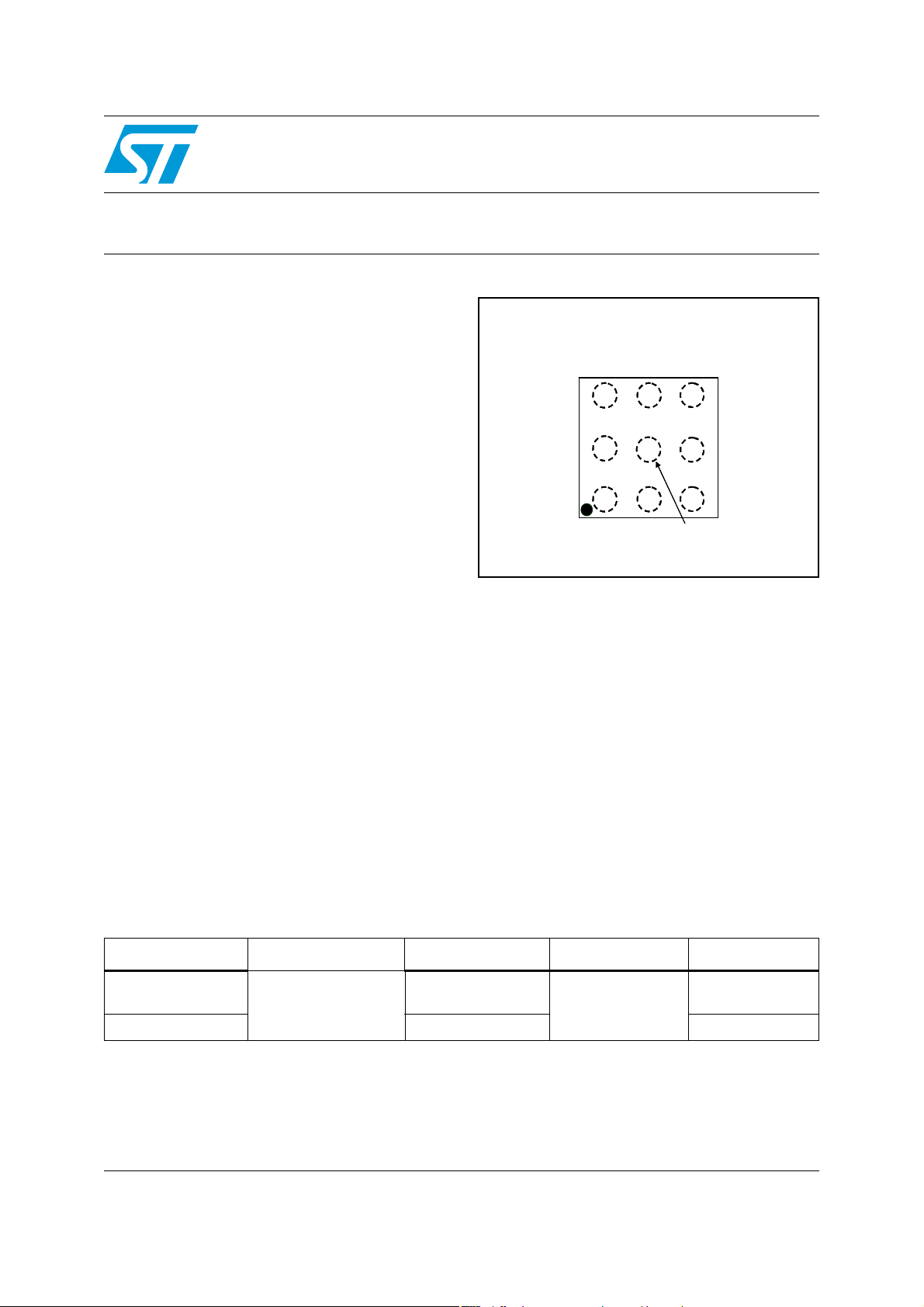
TS4994FC
with selectable standb y
TS4994EIJT - Flip-chip (9 bumps)
Gnd
Gnd
V
V
Bypass Stdby
Bypass Stdby
V
V
765
765
O-
O-
8
8
1
1
IN+
IN+
9
9
2
2
V
V
CC
CC
The device is equipped with common mode
feedback circu itry allowing outputs to be always
biased at V
/2 regardless of the input common
CC
mode voltage.
V
V
O+
O+
4
4
V
V
3
3
IN-
IN-
Stdby Mode
Stdby Mode
Description
The TS4994 is an audio power amplifier capable
The TS4994 is designed for high quality audio
applications such as mobile phones and requir es
few external components.
of delivering 1W of continuous RMS output power
into an 8Ω load @ 5V. Due to its differential input s,
Applications
it exhibits outstanding noise immunity.
An external standby mode control reduces the
supply current to less than 10nA. An STBY
MODE pin allows the standby to be active HIGH
or LOW. An internal thermal shutdown protection
is also provided, making the device capable of
■ Mobile phones (cellular / cordless)
■ Laptop / notebook computers
■ PDAs
■ Portable audio devices
sustaining short-circuits.
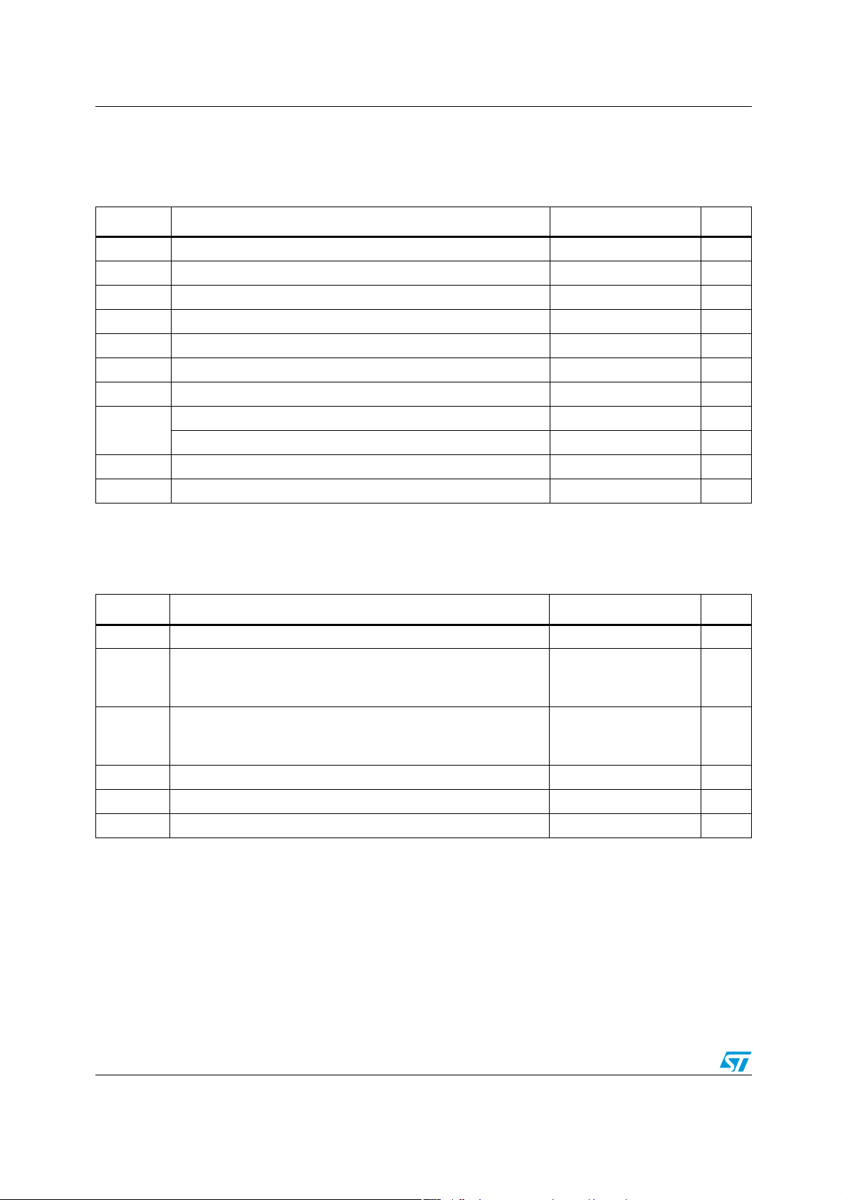
Order codes
Part number Temperature range Package Packaging Marking
TS4994EIKJT
-40°C, +85°C
TS4994EIJT Lead free flip-chip9 A94
FC9 with back
coating
Tape & reel
A94
December 2006 Rev 2 1/35
www.st.com
35

Contents TS4994FC
Contents
1 Application component information . . . . . . . . . . . . . . . . . . . . . . . . . . . . 3
2 Absolute maximum ratings and operating conditions . . . . . . . . . . . . . 4
3 Electrical characteristics . . . . . . . . . . . . . . . . . . . . . . . . . . . . . . . . . . . . . 5
4 Application information . . . . . . . . . . . . . . . . . . . . . . . . . . . . . . . . . . . . . 23
4.1 Differential configuration principle . . . . . . . . . . . . . . . . . . . . . . . . . . . . . . 23
4.2 Gain in typical application schematic . . . . . . . . . . . . . . . . . . . . . . . . . . . . 23
4.3 Common mode feedback loop limitations . . . . . . . . . . . . . . . . . . . . . . . . . 23
4.4 Low and high frequency response . . . . . . . . . . . . . . . . . . . . . . . . . . . . . . 24
4.5 Calculating the influence of mismatching on PSRR performance . . . . . . 25
4.6 CMRR performance . . . . . . . . . . . . . . . . . . . . . . . . . . . . . . . . . . . . . . . . . 27
4.7 Power dissipation and efficiency . . . . . . . . . . . . . . . . . . . . . . . . . . . . . . . 28
4.8 Decoupling of the circuit . . . . . . . . . . . . . . . . . . . . . . . . . . . . . . . . . . . . . . 30
4.9 Wake-up time: t
4.10 Shutdown time . . . . . . . . . . . . . . . . . . . . . . . . . . . . . . . . . . . . . . . . . . . . . 31
4.11 Pop performance . . . . . . . . . . . . . . . . . . . . . . . . . . . . . . . . . . . . . . . . . . . 31
4.12 Single-ended input configuration . . . . . . . . . . . . . . . . . . . . . . . . . . . . . . . 31
WU . . . . . . . . . . . . . . . . . . . . . . . . . . . . . . . . . . . . . . . . . . . . . . . . . . . . . . 30
5 Package information . . . . . . . . . . . . . . . . . . . . . . . . . . . . . . . . . . . . . . . . 32
6 Revision history . . . . . . . . . . . . . . . . . . . . . . . . . . . . . . . . . . . . . . . . . . . 34
2/35
TS4994FC Application component information
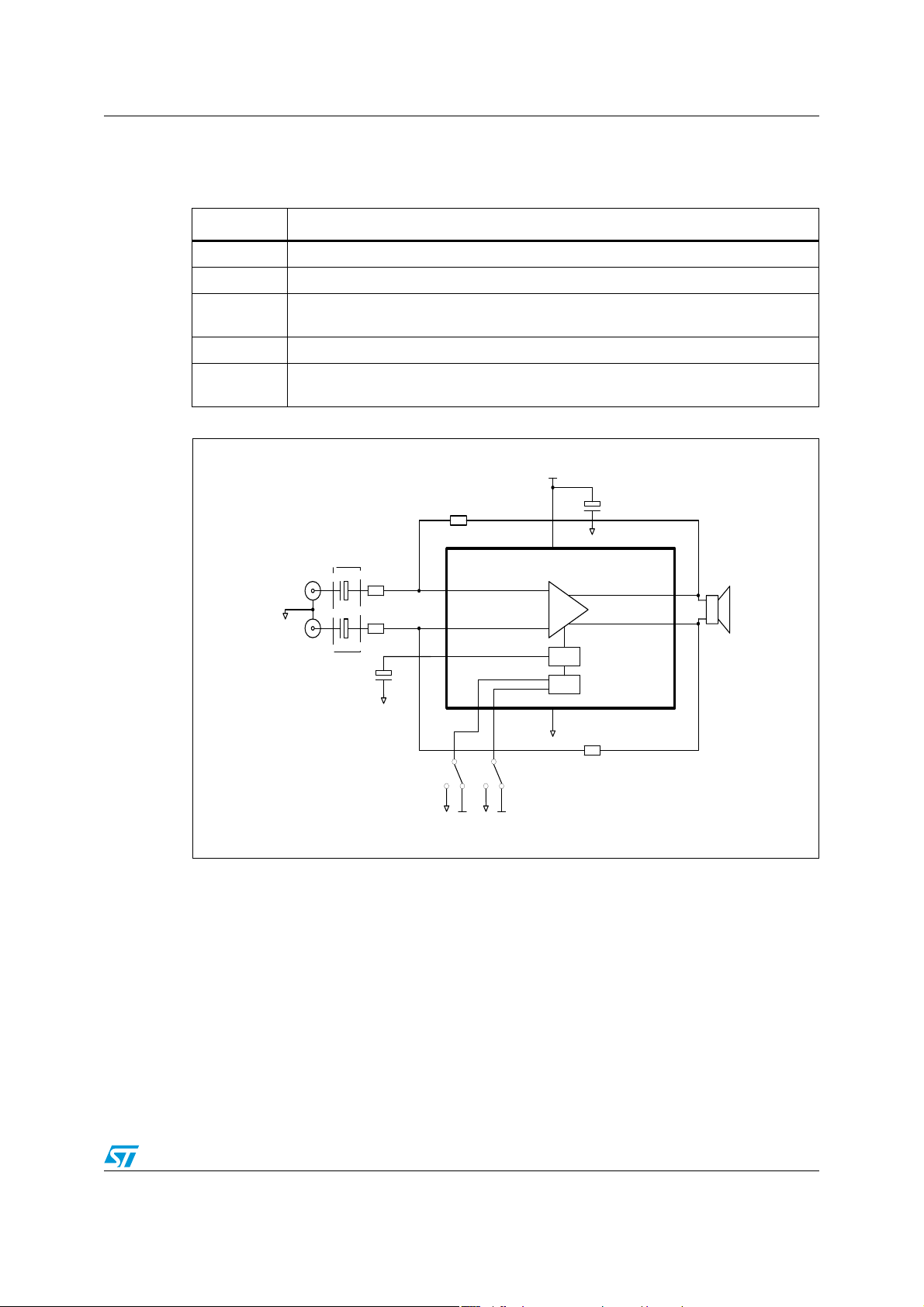
1 Application component information
Components Functional description
C
s
C
b
R
feed
R
in
C
in
Supply bypass capacitor that provides power supply filtering.
Bypass capacitor that provides half supply filtering.
Feedback resistor that sets the closed loop gain in conjunction with Rin
AV= closed loop gain = R
Inverting input resistor that sets the closed loop gain in conjunction with R
Optional input capacitor making a high pass filter together with Rin.
(FCL= 1/(2πRinCin).
Figure 1. Typical application
Diff. input -
GND
Diff. Input +
Cin1
+
220nF
Cin2
+
220nF
Optional
Rin1
20k
Rin2
20k
GND
+
Cb
1u
.
feed/Rin
VCC
+
Cs
Rfeed1
20k
Vin-
3
Vin+
1
Bypass
8
Mode Stdby TS4994IJ
4
2
VCC
-
+
Standby
GND
69
GND
1u
GND
Bias
Rfeed2
20k
Vo+
Vo-
.
feed
5
7
8 Ohms
GND GNDVCC VCC
3/35
Absolute maximum ratings and operating conditions TS4994FC
2 Absolute maximum ratings and operating conditions
Table 1. Absolute maximum ratings
Symbol Parameter Value Unit
(2)
(1)
(3)
6V
GND to V
CC
250 °C/W
V
T
T
R
P
CC
V
oper
stg
T
thja
diss
Supply voltage
Input voltage
i
Operating free air tempe rature range -40 to + 85 °C
Storage temperature -65 to +150 °C
Maximum junction temperature 150 °C
j
Thermal resistance junction to ambient
Power dissipation internally limited W
Human body model 2 kV
ESD
Machine model 200 V
Latch-up immunity 200 mA
Lead temperature (soldering, 10sec) 260 °C
1. All voltage values are measured with respect to the ground pin.
2. The magnitude of the input signal must never exceed V
3. The device is protected by a thermal shutdown active at 150°C.
Table 2. Operating conditions
+ 0.3V / GND - 0.3V.
CC
V
Symbol Parameter Value Unit
V
CC
Supply voltage 2.5 to 5.5 V
Standby mode voltage input:
V
SM
Standby active LOW
Standby active HIGH
=GND
V
SM
VSM=V
CC
Standby voltage input:
V
STBY
T
SD
R
L
R
thja
1. The minimum current consumption (I
temperature range.
Device ON (VSM= GND) or device OFF (VSM=VCC)
Device OFF (V
= GND) or device ON (VSM=VCC)
SM
Thermal shutdown temperature 150 °C
Load resistor ≥ 4 Ω
Thermal resistance junction to ambient 100 °C/W
) is guaranteed when V
STBY
=GND or VCC (i.e. supply rails) for the whole
STBY
1.5 ≤ V
GND
≤ V
STBY
STBY
≤ VCC
≤ 0.4
(1)
V
V
4/35
TS4994FC Electrical characteristics
3 Electrical characteristics
Table 3. Electrical characteristics for VCC = +5V, GND = 0V, T
= 25°C (unless otherwise
amb
specified)
Symbol Parameter Min. Typ. Max. Unit
I
CC
I
STBY
V
oo
V
ICM
P
out
THD + N
PSRR
CMRR
SNR
Supply current
No input signal, no load
Standby current
No input signal, V
No input signal, V
= VSM = GND, RL = 8Ω
STBY
= VSM = VCC, RL = 8Ω
STBY
Differential output offset voltage
No input signal, RL = 8Ω
Input common mode voltage
CMRR ≤ -60dB
Output power
THD = 1% Max, F= 1kHz, RL = 8Ω
Total harmonic distortion + noise
=850mW rms, AV=1, 20Hz ≤ F ≤ 20kHz, RL=8Ω
P
out
Power supply rejection ratio with inputs grounded
F = 217Hz, R = 8Ω, AV = 1, Cin = 4.7μF, Cb =1μF
IG
V
ripple
= 200mV
PP
Common mode rejection ratio
F = 217Hz, R
= 200mV
V
ic
= 8Ω, AV = 1, Cin = 4.7μF, Cb =1μF
L
PP
Signal-to-noise ratio (A-weighted filter, A
RL = 8Ω, THD +N < 0.7%, 20Hz ≤ F ≤ 20kHz
= 2.5)
V
(1)
47mA
10 1000 nA
0.1 10 mV
0.6 V
-0.9 V
CC
0.8 1.2 W
0.5 %
100 dB
90 dB
100 dB
GBP
Gain bandwidth product
R
= 8Ω
L
Output voltage noise, 20Hz ≤ F ≤ 20kHz, RL = 8Ω
Unweighted, A
A-weighted, A
Unweighted, A
V
N
A-weighted, A
Unweighted, A
A-weighted, A
= 1
V
= 1
V
= 2.5
V
= 2.5
V
= 7.5
V
= 7.5
V
Unweighted, Standby
A-weighted, Standby
t
WU
1. Dynamic measurements - 20*log(rms(V
2. Transition time from standby mode to fully operational amplifier.
Wake-up time
Cb =1μF
(2)
)/rms (V
out
ripple
)). V
ripple
5/35
2MHz
6
5.5
12
10.5
33
28
1.5
1
15 ms
is the super-imposed sinus signal relative to VCC.
μV
RMS
Electrical characteristics TS4994FC
Table 4. Electrical characteristics for VCC = +3.3V (all electrical values are guaranteed with
correlation measurements at 2.6V and 5V), GND = 0V, T
= 25°C (unless otherwise
amb
specified)
Symbol Parameter Min. Typ. Max. Unit
I
CC
I
STBY
V
oo
V
ICM
P
out
THD + N
PSRR
CMRR
SNR
Supply current no input signal, no load 3 7 mA
Standby current
No input signal, V
No input signal, V
= VSM = GND, RL = 8Ω
STBY
= VSM = VCC, RL = 8Ω
STBY
Differential output offset voltage
No input signal, RL = 8Ω
Input common mode voltage
CMRR ≤ -60dB
Output power
THD = 1% max, F= 1kHz, R
= 8Ω
L
Total harmonic distortion + noise
= 300mW rms, AV = 1, 20Hz ≤ F ≤ 20kHz, RL = 8Ω
P
out
Power supply rejection ratio with inputs grounded
F = 217Hz, R = 8Ω, AV = 1, Cin = 4.7μF, Cb =1μF
IG
V
ripple
= 200mV
PP
0.6 V
300 500 mW
(1)
10 1000 nA
0.1 10 mV
-0.9 V
CC
0.5 %
100 dB
Common mode rejection ratio
F = 217Hz, R
= 200mV
V
ic
Signal-to-noise ratio (A-weighted filter, A
RL = 8Ω, THD +N < 0.7%, 20Hz ≤ F ≤ 20kHz
= 8Ω, AV = 1, Cin = 4.7μF, Cb =1μF
L
PP
= 2.5)
V
90 dB
100 dB
GBP
Gain bandwidth product
R
= 8Ω
L
Output voltage noise, 20Hz ≤ F ≤ 20kHz, RL = 8Ω
Unweighted, A
V
= 1
A-weighted, AV = 1
V
N
A-weighted, A
Unweighted, A
A-weighted, A
Unweighted, A
= 2.5
V
= 2.5
V
= 7.5
V
= 7.5
V
Unweighted, Standby
A-weighted, Standby
t
WU
1. Dynamic measurements - 20*log(rms(V
2. Transition time from standby mode to fully operational amplifier.
Wake-up time
Cb =1μF
(2)
)/rms (V
out
ripple
)). V
ripple
2MHz
6
5.5
12
10.5
33
28
1.5
1
15 ms
is the super-imposed sinus signal relative to VCC.
μV
RMS
6/35
TS4994FC Electrical characteristics
Table 5. Electrical characteristics for VCC = +2.6V, GND = 0V, T
= 25°C (unless otherwise
amb
specified)
Symbol Parameter Min. Typ. Max. Unit
I
CC
I
STBY
V
V
ICM
P
out
THD + N
PSRR
CMRR
SNR
GBP
V
t
WU
Supply current
No input signal, no load
Standby current
No input signal, V
No input signal, V
Differential output offset voltage
oo
No input signal, R
= VSM = GND, RL = 8Ω
STBY
= VSM = VCC, RL = 8Ω
STBY
= 8Ω
L
Input common mode voltage
CMRR ≤ -60dB
Output power
THD = 1% max, F= 1kHz, RL = 8Ω
Total harmonic distortion + noise
= 225mW rms, AV = 1, 20Hz ≤ F ≤ 20kHz, RL = 8Ω
P
out
Power supply rejection ratio with inputs grounded
F = 217Hz, R = 8Ω, AV = 1, Cin = 4.7μF, Cb =1μF
IG
V
= 200mV
ripple
PP
Common mode rejection ratio
F = 217Hz, R
Vic = 200mV
= 8Ω, AV = 1, Cin = 4.7μF, Cb =1μF
L
PP
Signal-to-noise ratio (A-weighted filter, A
= 8Ω, THD +N < 0.7%, 20Hz ≤ F ≤ 20kHz
R
L
Gain bandwidth product
= 8Ω
R
L
Output voltage noise, 20Hz ≤ F ≤ 20kHz, RL = 8Ω
Unweighted, AV = 1
A-weighted, A
V
= 1
Unweighted, AV = 2.5
N
A-weighted, A
Unweighted, A
A-weighted, A
= 2.5
V
= 7.5
V
= 7.5
V
Unweighted, Standby
A-weighted, Standby
Wake-up time
(2)
Cb =1μF
= 2.5)
V
(1)
37mA
10 1000 nA
0.1 10 mV
0.6 V
- 0.9 V
CC
200 300 mW
0.5 %
100 dB
90 dB
100 dB
2MHz
6
5.5
12
10.5
33
28
1.5
1
15 ms
μV
RMS
1. Dynamic measurements - 20*log(rms(V
2. Transition time from standby mode to fully operational amplifier.
)/rms (V
out
ripple
)). V
ripple
7/35
is the super-imposed sinus signal relative to VCC.
Electrical characteristics TS4994FC
0.0 0.6 1.2 1.8 2.4
0.0
0.5
1.0
1.5
2.0
2.5
3.0
Standby mode=0V
Standby mode=2.6V
Vcc = 2.6V
No load
Tamb=25°C
Current Consumption (mA)
Standby Voltage (V)
0.0 0.2 0.4 0.6 0.8 1.0 1.2 1.4 1.6
0.0
0.2
0.4
0.6
0.8
1.0
1.2
1.4
RL=16
Ω
RL=8
Ω
Vcc=5V
F=1kHz
THD+N<1%
RL=4
Ω
Power Dissipation (W)
Output Power (W)
Figure 2. Current consumption vs. power
supply voltage
4.0
No load
Tamb=25°C
3.5
3.0
2.5
2.0
1.5
1.0
Current Consumption (mA)
0.5
0.0
012345
Power Supply Voltage (V)
Figure 4. Current consumption vs. standby
voltage
3.5
3.0
2.5
2.0
1.5
1.0
Current Consumption (mA)
0.5
0.0
0.0 0.6 1.2 1.8 2.4 3.0
Standby mode=0V
Standby mode=3.3V
Standby Voltage (V)
Vcc = 3.3V
No load
Tamb=25°C
Figure 3. Current consumption vs. standby
voltage
4.0
3.5
3.0
2.5
2.0
1.5
1.0
Current Consumption (mA)
0.5
0.0
012345
Standby mode=5V
Standby mode=0V
Standby Voltage (V)
Vcc = 5V
No load
Tamb=25°C
Figure 5. Current consumption vs. standby
voltage
Figure 6. Differential DC output voltage vs.
common mode input voltage
1000
Av = 1
Tamb = 25°C
100
10
Voo (mV)
1
0.1
0.01
0.0 0.5 1.0 1.5 2.0 2.5 3.0 3.5 4.0 4.5 5.0
8/35
Vcc=2.5V
Common Mode Input Voltage (V)
Figure 7. Power dissipation vs. output power
Vcc=3.3V
Vcc=5V
TS4994FC Electrical characteristics
0.0 0.1 0.2 0.3 0.4
0.00
0.05
0.10
0.15
0.20
0.25
0.30
0.35
0.40
RL=4
Ω
RL=8
Ω
Vcc=2.6V
F=1kHz
THD+N<1%
RL=16
Ω
Power Dissipation (W)
Output Power (W)
2.5 3.0 3.5 4.0 4.5 5.0 5.5
0.0
0.2
0.4
0.6
0.8
1.0
1.2
1.4
1.6
1.8
2.0
THD+N=10%
RL = 8
Ω
F = 1kHz
BW < 125kHz
Tamb = 25°C
THD+N=1%
Output power (W)
Vcc (V)
2.5 3.0 3.5 4.0 4.5 5.0 5.5
0.0
0.1
0.2
0.3
0.4
0.5
0.6
THD+N=10%
RL = 32
Ω
F = 1kHz
BW < 125kHz
Tamb = 25°C
THD+N=1%
Output power (W)
Vcc (V)
Figure 8. Power dissipation vs. outpu t power Figure 9. Power dissipation vs. output power
0.6
Vcc=3.3V
F=1kHz
0.5
THD+N<1%
0.4
0.3
0.2
Power Dissipation (W)
0.1
0.0
0.0 0.1 0.2 0.3 0.4 0.5 0.6 0.7
RL=16
Ω
Output Power (W)
Figure 10. Output power vs. power supply
voltage
2.4
RL = 4
2.2
2.0
1.8
1.6
1.4
1.2
1.0
0.8
Output power (W)
0.6
0.4
0.2
0.0
Ω
F = 1kHz
BW < 125kHz
Tamb = 25°C
2.5 3.0 3.5 4.0 4.5 5.0 5.5
THD+N=10%
Vcc (V)
RL=8
Ω
THD+N=1%
RL=4
Ω
Figure 11. Output power vs. power supply
voltage
Figure 12. Output power vs. power supply
voltage
1.2
RL = 16
Ω
F = 1kHz
1.0
BW < 125kHz
Tamb = 25°C
0.8
0.6
0.4
Output power (W)
0.2
0.0
2.5 3.0 3.5 4.0 4.5 5.0 5.5
THD+N=10%
Figure 13. Output power vs. power supply
voltage
THD+N=1%
Vcc (V)
9/35
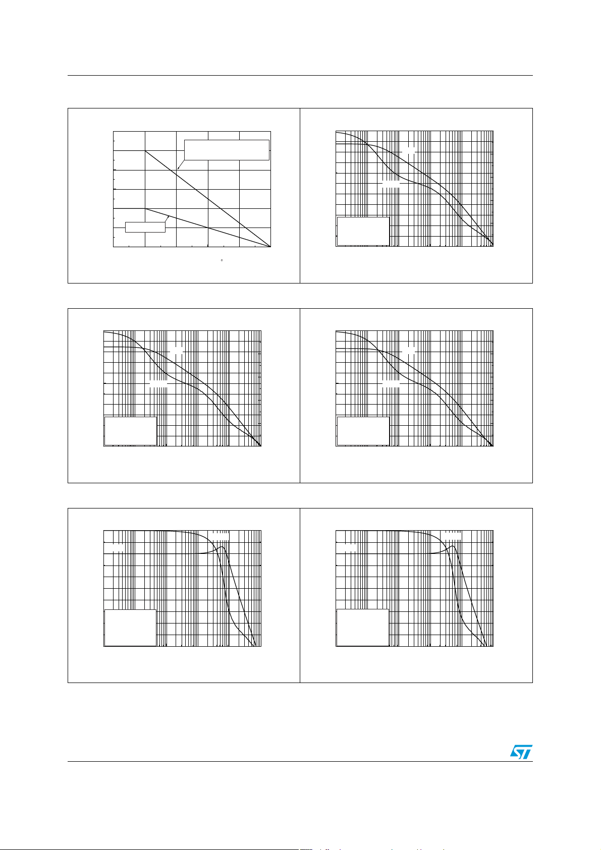
Electrical characteristics TS4994FC
Figure 14. Power derating curves Figure 15. Open loop gain vs. frequency
1.2
1.0
0.8
0.6
0.4
No Heat sink
0.2
Flip-Chip Package Power Dissipation (W)
0.0
0 25 50 75 100 125
Ambiant Temperature ( C)
Heat sink surface ≈ 100mm
(See demoboard)
2
60
40
20
Gain (dB)
0
Vcc = 5V
-20
ZL = 8Ω + 500pF
Tamb = 25°C
-40
0.1 1 10 100 1000 10000
Gain
Phase
Frequency (kHz)
Figure 16. Open loop gain vs. frequency Figure 17. Open loop gain vs. frequency
0
60
40
20
Gain (dB)
0
Phase
Gain
-40
-80
-120
Phase (°)
60
40
20
Gain (dB)
0
Gain
Phase
0
-40
-80
-120
-160
-200
0
-40
-80
-120
Phase (°)
Phase (°)
Vcc = 3.3V
-20
ZL = 8Ω + 500pF
Tamb = 25°C
-40
0.1 1 10 100 1000 10000
Frequency (kHz)
-160
-200
Vcc = 2.6V
-20
ZL = 8Ω + 500pF
Tamb = 25°C
-40
0.1 1 10 100 1000 10000
Frequency (kHz)
-160
-200
Figure 18. Closed loop gain vs. frequency Figure 19. Closed loop gain vs. frequency
10
Gain
0
-10
-20
Gain (dB)
Vcc = 5V
-30
Av = 1
ZL = 8Ω + 500pF
Tamb = 25°C
-40
0.1 1 10 100 1000 10000
Frequency (kHz)
Phase
0
-40
-80
-120
-160
-200
10
Gain
0
-10
Phase (°)
-20
Gain (dB)
Vcc = 3.3V
-30
Av = 1
ZL = 8Ω + 500pF
Tamb = 25°C
-40
0.1 1 10 100 1000 10000
Frequency (kHz)
Phase
0
-40
-80
-120
-160
-200
Phase (°)
10/35
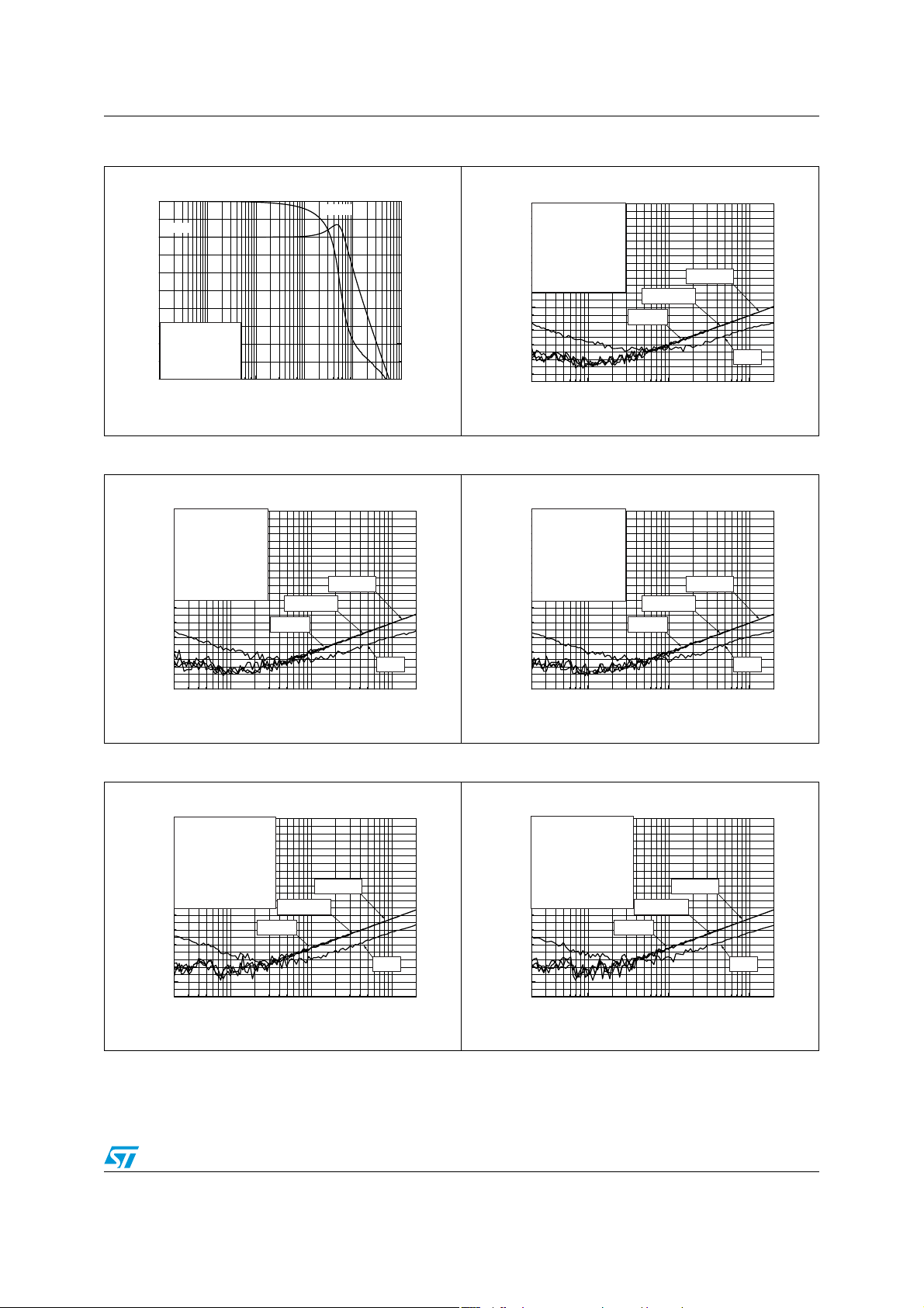
TS4994FC Electrical characteristics
100 1000 10000
-120
-110
-100
-90
-80
-70
-60
-50
-40
-30
-20
-10
0
Cb=0.1μF
Cb=1μF
Cb=0
20k
20
Cb=0.47μF
Vcc = 5V
Vripple = 200mVpp
Inputs = Grounded
Av = 1, Cin = 4.7μF
RL ≥ 8
Ω
Tamb = 25°C
PSRR (dB)
Frequency (Hz)
100 1000 10000
-120
-110
-100
-90
-80
-70
-60
-50
-40
-30
-20
-10
0
Cb=0.1μF
Cb=1μF
Cb=0
20k
20
Cb=0.47μF
Vcc = 2.6V
Vripple = 200mVpp
Inputs = Grounded
Av = 1, Cin = 4.7μF
RL ≥ 8
Ω
Tamb = 25°C
PSRR (dB)
Frequency (Hz)
100 1000 10000
-120
-110
-100
-90
-80
-70
-60
-50
-40
-30
-20
-10
0
Cb=0.1μF
Cb=1μF
Cb=0
20k
20
Cb=0.47μF
Vcc = 3.3V
Vripple = 200mVpp
Inputs = Grounded
Av = 2.5, Cin = 4.7μF
RL ≥ 8
Ω
Tamb = 25°C
PSRR (dB)
Frequency (Hz)
Figure 20. Closed loop gain vs. frequency Figure 21. PSRR vs. frequency
10
Gain
0
-10
-20
Gain (dB)
Vcc = 2.6V
-30
Av = 1
ZL = 8Ω + 500pF
Tamb = 25°C
-40
0.1 1 10 100 1000 10000
Frequency (kHz)
Phase
0
-40
-80
-120
-160
-200
Phase (°)
Figure 22. PSRR vs. frequency Figure 23. PSRR vs. frequency
0
-10
Vcc = 3.3V
Vripple = 200mVpp
-20
Inputs = Grounded
-30
Av = 1, Cin = 4.7μF
-40
RL ≥ 8
-50
-60
-70
PSRR (dB)
-80
-90
-100
-110
-120
Tamb = 25°C
20
Ω
Cb=1μF
100 1000 10000
Frequency (Hz)
Cb=0.1μF
Cb=0.47μF
Cb=0
20k
Figure 24. PSRR vs. frequency Figure 25. PSRR vs. frequency
0
-10
Vcc = 5V
Vripple = 200mVpp
-20
Inputs = Grounded
-30
Av = 2.5, Cin = 4.7μF
-40
RL ≥ 8
Tamb = 25°C
20
Ω
100 1000 10000
-50
-60
-70
PSRR (dB)
-80
-90
-100
-110
-120
Cb=1μF
Frequency (Hz)
Cb=0.47μF
Cb=0.1μF
Cb=0
20k
11/35
 Loading...