

ST TS488, TS489 User Manual
TS488
TS489
Pop-free 120 mW stereo headphone amplifier
Datasheet − production data
Features
■ Pop and click noise protection circuitry
■ Operating range from V
■ Standby mode active low (TS488) or high (TS489)
■ Output power:
– 120 mW at 5 V, into 16 Ω
with 0.1% THD+N max (1 kHz)
– 55 mW at 3.3 V, into 16 Ω
with 0.1% THD+N max (1 kHz)
■ Low current consumption: 2.7 mA max at 5 V
■ Ultra-low standby current consumption: 10 nA
typical
■ High signal-to-noise ratio
■ High crosstalk immunity: 102 dB (F = 1 kHz)
■ PSRR: 70 dB typ. (F = 1 kHz), inputs grounded
at 5 V
■ Unity-gain stable
■ Short-circuit protection circuitry
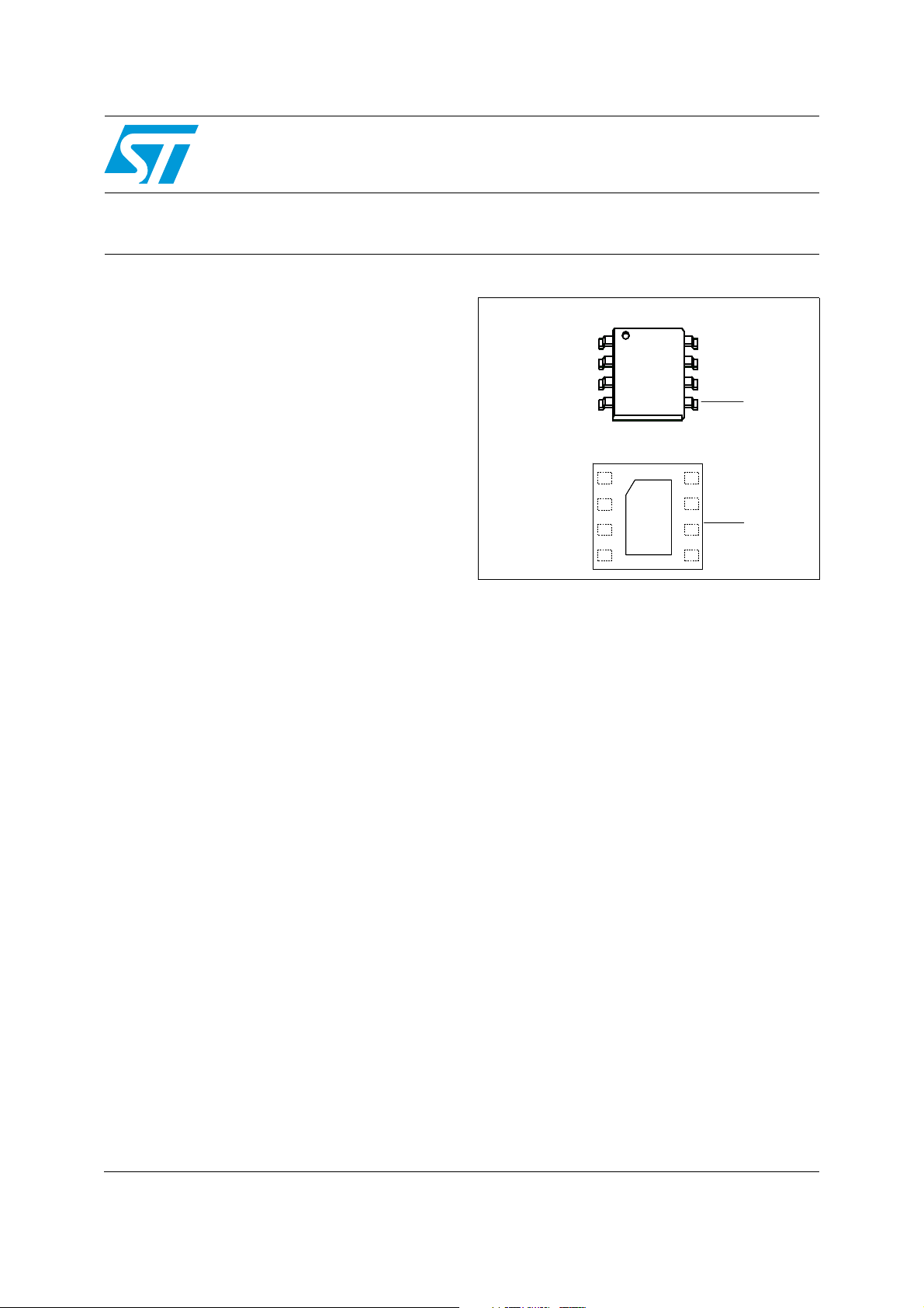
■ Available in lead-free MiniSO-8 & DFN8
2 mm x 2 mm
= 2.2 V to 5.5 V
CC
TS488IST - MiniSO-8
OUT (1 )
OUT (1 )
OUT (1 )
VIN (1)
VIN (1)
VIN (1)
BYPASS
BYPASS
BYPASS
GND
GND
GND
1
1
1
2
2
2
3
3
3
4
4
4
8
8
8
7
7
7
6
6
6
5
5
5
VCC
VCC
VCC
OUT (2 )
OUT (2 )
OUT (2 )
VIN (2)
VIN (2)
VIN (2)
SHUTDOWN
SHUTDOWN
SHUTDOWN
TS488IQT - DFN8
Vcc
Vcc
Vcc
OUT (1)
OUT (1)
OUT (1)
VIN (1)
VIN (1)
VIN (1)
Bypass
Bypass
Bypass
1
1
11
2
2
22
3
3
33
4
4
44
8
8
88
7
7
77
6
6
66
5
5
55
OUT
OUT
OUT
(2)
(2)
(2)
VIN (2)
VIN (2)
VIN (2)
Shutdown
Shutdown
Shutdown
GND
GND
GND
Applications
■ Headphone amplifiers
■ Mobile phones, PDAs, computer motherboards
■ High-end TVs, portable audio players
Description
The TS488/9 is an enhancement of TS486/7 that
eliminates pop and click noise and reduces the
number of external passive components.
The TS488/9 is a dual audio power amplifier
capable of driving, in single-ended mode, either a
16 Ω or a 32 Ω stereo headset.
Capable of descending to low voltages, it delivers
up to 31 mW per channel (into 16 Ω loads) of
continuous average power with 0.1% THD+N in
the audio bandwidth from a 2.5 V power supply.
An externally-controlled standby mode reduces
the supply current to 10 nA (typ.). The unity gain
stable TS488/9 is configured by external gainsetting resistors.
May 2012 Doc ID 11971 Rev 5 1/32
This is information on a product in full production.
www.st.com
32

Contents TS488-TS489
Contents
1 Typical application schematic . . . . . . . . . . . . . . . . . . . . . . . . . . . . . . . . . 3
2 Absolute maximum ratings and operating conditions . . . . . . . . . . . . . 4
3 Electrical characteristics . . . . . . . . . . . . . . . . . . . . . . . . . . . . . . . . . . . . . 5
4 Application information . . . . . . . . . . . . . . . . . . . . . . . . . . . . . . . . . . . . . 22
4.1 Power dissipation and efficiency . . . . . . . . . . . . . . . . . . . . . . . . . . . . . . . 22
4.2 Total power dissipation . . . . . . . . . . . . . . . . . . . . . . . . . . . . . . . . . . . . . . . 23
4.3 Lower cutoff frequency . . . . . . . . . . . . . . . . . . . . . . . . . . . . . . . . . . . . . . . 23
4.4 Higher cutoff frequency . . . . . . . . . . . . . . . . . . . . . . . . . . . . . . . . . . . . . . 24
4.5 Gain setting . . . . . . . . . . . . . . . . . . . . . . . . . . . . . . . . . . . . . . . . . . . . . . . 25
4.6 Decoupling of the circuit . . . . . . . . . . . . . . . . . . . . . . . . . . . . . . . . . . . . . . 25
4.7 Standby mode . . . . . . . . . . . . . . . . . . . . . . . . . . . . . . . . . . . . . . . . . . . . . 25
4.8 Wake-up time . . . . . . . . . . . . . . . . . . . . . . . . . . . . . . . . . . . . . . . . . . . . . . 26
4.9 POP performance . . . . . . . . . . . . . . . . . . . . . . . . . . . . . . . . . . . . . . . . . . . 26
Connecting the headphones . . . . . . . . . . . . . . . . . . . . . . . . . . . . . . . . . . . . . . . . . 27
5 Package mechanical data . . . . . . . . . . . . . . . . . . . . . . . . . . . . . . . . . . . . 28
5.1 MiniSO-8 package . . . . . . . . . . . . . . . . . . . . . . . . . . . . . . . . . . . . . . . . . . 28
5.2 DFN8 package . . . . . . . . . . . . . . . . . . . . . . . . . . . . . . . . . . . . . . . . . . . . . 29
6 Ordering information . . . . . . . . . . . . . . . . . . . . . . . . . . . . . . . . . . . . . . . 30
7 Revision history . . . . . . . . . . . . . . . . . . . . . . . . . . . . . . . . . . . . . . . . . . . 31
2/32 Doc ID 11971 Rev 5
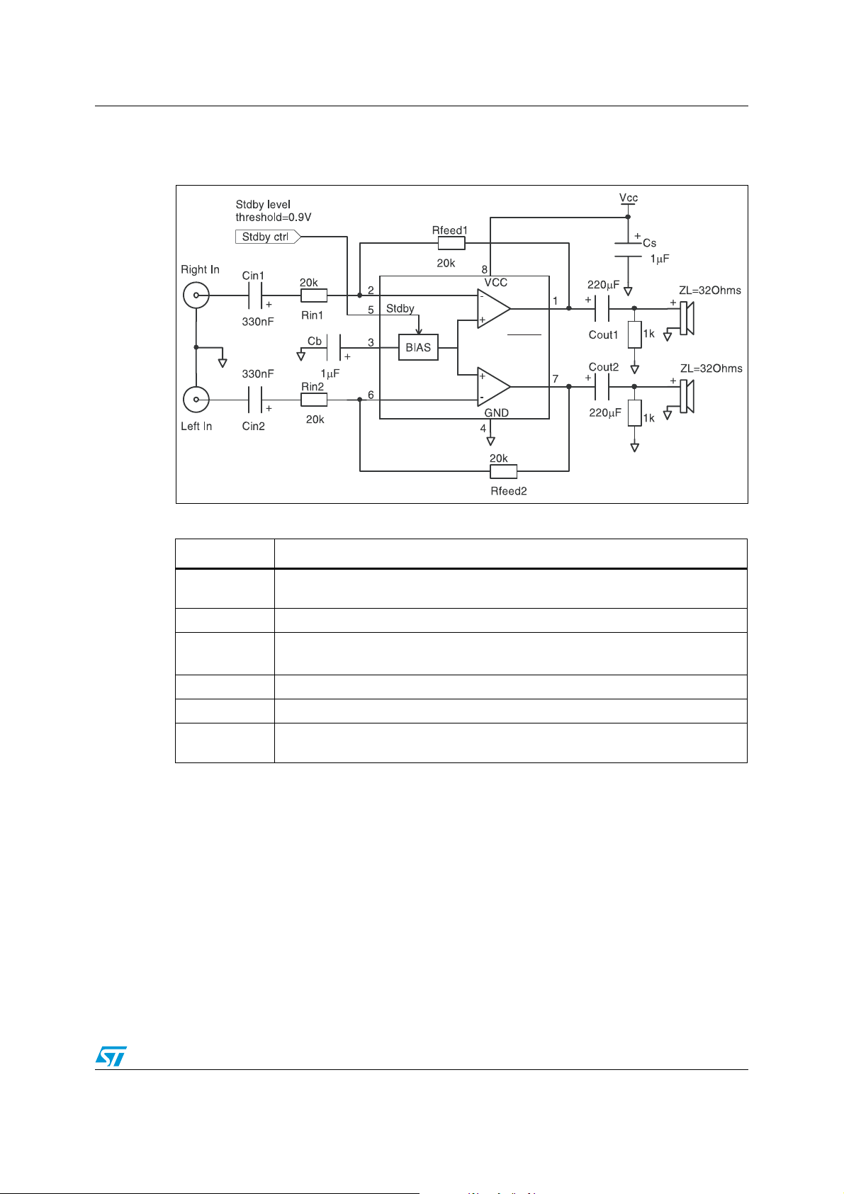
TS488-TS489 Typical application schematic
1 Typical application schematic
Figure 1. Typical application for the TS488-TS489
TS488=stdby
TS489=stdby
Table 1. Application component information
Component Functional description
R
C
R
feed1,2
C
out1,2
in1,2
in1,2
C
s
C
b
Inverting input resistor that sets the closed loop gain in conjunction with R
This resistor also forms a high pass filter with Cin (F
Input coupling capacitor that blocks the DC voltage at the amplifier’s input terminal.
Feedback resistor that sets the closed loop gain in conjunction with Rin.
AV= Closed Loop Gain= -R
feed/Rin
.
Supply output capacitor that provides power supply filtering.
Bypass capacitor that provides half supply filtering.
Output coupling capacitor that blocks the DC voltage at the load input terminal.
This capacitor also forms a high pass with R
(F
L
= 1 / (2 x Pi x R
c
= 1 / (2 x Pi x R
c
x C
L
x Cin)).
in
out
)).
feed
.
Doc ID 11971 Rev 5 3/32
Absolute maximum ratings and operating conditions TS488-TS489
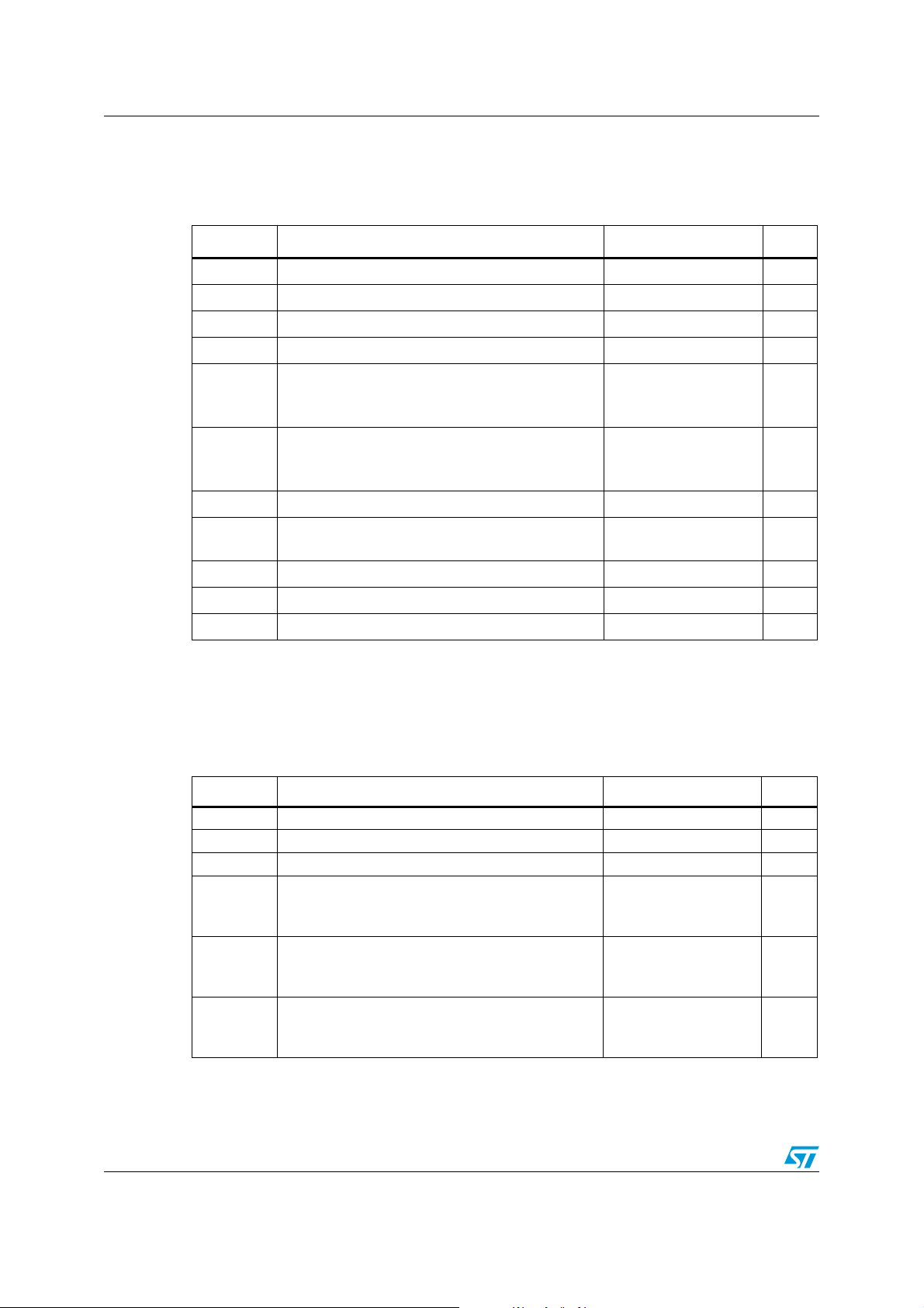
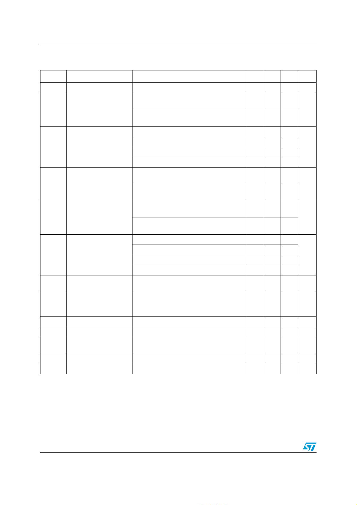
2 Absolute maximum ratings and operating conditions
Table 2. Absolute maximum ratings
Symbol Parameter Value Unit
V
CC
V
T
stg
T
Supply voltage
Input voltage -0.3 V to V
i
Storage temperature -65 to +150 °C
Maximum junction temperature 150 °C
j
Thermal resistance junction-to-ambient
R
thja
MiniSO-8
DFN8
Power dissipation
P
diss
MiniSO-8
DFN8
ESD Human body model (pin to pin) 2 kV
ESD
Machine model
220 pF - 240 pF (pin to pin)
(1)
(2)
6V
+0.3 V V
CC
215
°C/W
70
:
0.58
W
1.79
200 V
Latch-up Latch-up immunity (all pins) 200 mA
Lead temperature (soldering, 10 sec) 250 °C
Output short-circuit to V
1. All voltage values are measured with respect to the ground pin.
2. P
3. Attention must be paid to continuous power dissipation (VDD x 250 mA). Short-circuits can cause
Table 3. Operating conditions
is calculated with T
diss
excessive heating and destructive dissipation. Exposing the IC to a short-circuit for an extended period of
time will dramatically reduce the product’s life expectancy.
= 25 °C, Tj= 150 °C.
amb
or GND continuous
CC
(3)
Symbol Parameter Value Unit
V
T
CC
R
oper
Supply voltage 2.2 to 5.5 V
Load resistor ≥ 16 Ω
L
Operating free air temperature range -40 to + 85 °C
Load capacitor:
C
L
= 16 to 100 Ω
R
L
RL > 100 Ω
400
100
Standby voltage input:
V
STBY
TS488 active, TS489 in standby
TS488 in standby, TS489 active
1.5 ≤ V≤ V
GND ≤ V
STBY
CC
≤ 0.4
(1)
Thermal resistance junction-to-ambient
R
thja
1. The minimum current consumption (I
temperature range.
2. When mounted on a 4-layer PCB.
MiniSO-8
(2)
DFN8
190
40
) is guaranteed at GND (TS488) or VCC (TS489) for the whole
STBY
pF
V
°C/W
4/32 Doc ID 11971 Rev 5
TS488-TS489 Electrical characteristics
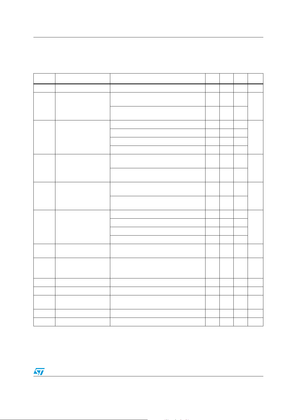
3 Electrical characteristics
Table 4. Electrical characteristics at VCC=+5 V
with GND = 0 V, T
= 25 °C (unless otherwise specified)
amb
Symbol Parameter Conditions Min. Typ. Max. Unit
I
I
STBY
P
THD+N
PSRR
V
SNR Signal-to-noise ratio
Supply current No input signal, no load 2 2.7 mA
CC
No input signal, V
RL = 32 Ω
= GND for TS488,
STBY
10 1000
Standby current
Output power
out
Total harmonic distortion
+ noise
Power supply rejection
ratio, inputs grounded
Output swing
O
No input signal, V
STBY=VCC
RL = 32 Ω
THD+N = 0.1% max, F = 1 kHz, R
THD+N = 1% max, F = 1 kHz, R
THD+N = 0.1% max, F = 1 kHz, R
THD+N = 1% max, F = 1 kHz, R
=-1, RL=32 Ω, P
A
V
out
20 Hz ≤ F ≤ 20 kHz
A
=-1, RL=16 Ω, P
V
out
20 Hz ≤ F ≤ 20 kHz
AV=-1, RL ≥ 16 Ω, Cb=1 µF, F = 1 kHz,
= 200 mVpp
V
ripple
(1)
=-1, RL ≥ 16 Ω, Cb=1 µF, F = 217 Hz,
A
V
V
= 200 mVpp
ripple
: RL=32 Ω 0.23 0.31
V
OL
V
: RL= 32 Ω 4.53 4.72
OH
: RL=16 Ω 0.44 0.57
V
OL
V
: RL= 16 Ω 4.18 4.48
OH
A-weighted, A
=-1, RL=32 Ω,
V
THD+N < 0.4%, 20 Hz ≤ F ≤ 20 kHz
for TS489,
=60 mW,
=90 mW,
=32 Ω 75
L
=32 Ω 70 80
L
=16 Ω 120
L
=16 Ω 100 130
L
64 70
62 68
10 1000
0.3
0.3
105 dB
nA
mW
%
dB
V
Crosstalk Channel separation
Input capacitance 1 pF
C
i
GBP Gain bandwidth product R
SR
V
t
1. Guaranteed by design and evaluation.
Slew rate, unity gain
inverting
Input offset voltage V
IO
Wake-up time 100 ms
wu
R
= 32 Ω, AV=-1
L
F = 1 kHz
F = 20 Hz to 20 kHz
= 32 Ω 1.1 MHz
L
-102
-84
dB
RL= 16 Ω 0.65 V/μs
icm=VCC
/2 1 20 mV
Doc ID 11971 Rev 5 5/32
Electrical characteristics TS488-TS489
Table 5. Electrical characteristics at VCC=+3.3 V
with GND = 0 V, T
= 25 °C (unless otherwise specified)
amb
(1)
Symbol Parameter Conditions Min. Typ. Max. Unit
I
I
STBY
P
THD+N
PSRR
V
SNR Signal-to-noise ratio
Supply current No input signal, no load 1.8 2.5 mA
CC
No input signal, V
RL = 32 Ω
= GND for TS488,
STBY
10 1000
Standby current
Output power
out
Total harmonic distortion
+ noise
Power supply rejection
ratio, inputs grounded
Output swing
O
No input signal, V
STBY=VCC
RL = 32 Ω
THD+N = 0.1% max, F = 1 kHz, R
THD+N = 1% max, F = 1 kHz, R
THD+N = 0.1% max, F = 1 kHz, R
THD+N = 1% max, F = 1 kHz, R
=-1, RL=32 Ω, P
A
V
out
20 Hz ≤ F ≤ 20 kHz
=-1, RL=16 Ω, P
A
V
out
20 Hz ≤ F ≤ 20 kHz
AV=-1, RL ≥ 16 Ω, Cb=1 µF, F = 1 kHz,
= 200 mVpp
V
ripple
(2)
=-1, RL ≥ 16 Ω, Cb=1 µF, F = 217 Hz,
A
V
V
= 200 mVpp
ripple
: RL=32 Ω 0.15 0.2
V
OL
V
: RL=32 Ω 3.03 3.12
OH
: RL=16 Ω 0.28 0.36
V
OL
V
: RL=16 Ω 2.82 2.97
OH
A-weighted, A
=-1, RL=32 Ω,
V
THD+N < 0.4%, 20 Hz ≤F ≤ 20 kHz
for TS489,
= 16 mW,
= 35 mW,
=32 Ω 34
L
=32 Ω 30 35
L
=16 Ω 55
L
=16 Ω 47 57
L
63 69
61 67
10 1000
0.3
0.3
102 dB
nA
mW
%
dB
V
R
=32 Ω, AV=-1
Crosstalk Channel separation
L
F = 1 kHz
F = 20 Hz to 20 kHz
Input capacitance 1 pF
C
i
GBP Gain bandwidth product R
SR
V
t
1. All electrical values are guaranteed with correlation measurements at 2.5 V and 5 V.
2. Guaranteed by design and evaluation.
Slew rate, unity gain
inverting
Input offset voltage V
IO
Wake-up time 100 ms
wu
=32 Ω 1.1 MHz
L
RL=16 Ω 0.6 V/μs
icm=VCC
/2 1 20 mV
6/32 Doc ID 11971 Rev 5
-102
-84
dB

TS488-TS489 Electrical characteristics
Table 6. Electrical characteristics at VCC=+2.5 V
with GND = 0 V, T
Symbol Parameter Conditions Min. Typ. Max. Unit
= 25 °C (unless otherwise specified)
amb
I
I
STBY
P
THD+N
PSRR
V
Supply current No input signal, no load 1.8 2.5 mA
CC
Standby current
Output power
out
Total harmonic distortion
+ noise
Power supply rejection
ratio, inputs grounded
Output swing
O
SNR Signal-to-noise ratio
Crosstalk Channel separation
No input signal, V
= GND for TS488,
STBY
RL = 32 Ω
No input signal, V
= 32 Ω
R
L
STBY=VCC
THD+N = 0.1% max, F = 1 kHz, R
THD+N = 1% max, F = 1 kHz, R
THD+N = 0.1% max, F = 1 kHz, R
THD+N = 1% max, F = 1 kHz, R
A
= -1, RL=32 Ω, P
V
= 10 mW,
out
20 Hz ≤ F ≤ 20 kHz
=-1, RL=16 Ω, P
A
V
= 16 mW,
out
20 Hz ≤ F ≤ 20 kHz
AV = -1, RL ≥ 16 Ω, Cb=1 µF, F = 1 kHz,
V
= 200 mVpp
ripple
(1)
A
= -1, RL ≥ 16 Ω, Cb=1 µF, F = 217 Hz,
V
V
= 200 mVpp
ripple
: RL=32 Ω 0.12 0.16
V
OL
V
: RL=32 Ω 2.3 2.36
OH
: RL=16 Ω 0.22 0.28
V
OL
: RL=16 Ω 2.15 2.25
V
OH
A-weighted, A
= -1, RL=32 Ω,
V
THD+N < 0.4%, 20 Hz ≤ F ≤ 20 kHz
=32 Ω, AV = -1
R
L
F = 1 kHz
F = 20 Hz to 20 kHz
for TS489,
=32 Ω 19
L
=32 Ω 18 20
L
=16 Ω 31
L
=16 Ω 27 32
L
10 1000
10 1000
mW
0.3
0.3
68
66
100 dB
-102
-84
nA
%
dB
V
dB
Input capacitance 1 pF
C
i
GBP Gain bandwidth product R
SR
V
t
1. Guaranteed by design and evaluation.
Slew rate, unity gain
inverting
Input offset voltage V
IO
Wake-up time 100 ms
wu
=32 Ω 1.1 MHz
L
=16 Ω 0.6 V/μs
R
L
= VCC/2 1 20 mV
icm
Doc ID 11971 Rev 5 7/32
Electrical characteristics TS488-TS489
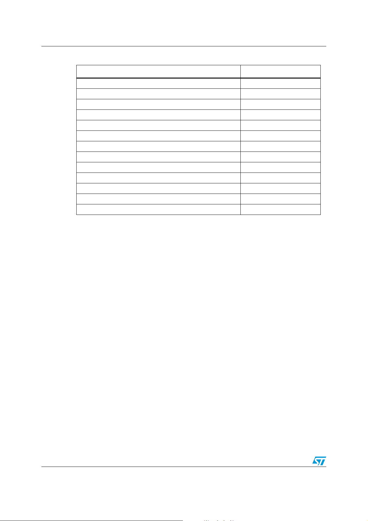
Table 7. Index of graphics
Description Figure
Open-loop frequency response Figure 2 to Figure 11
Power derating curves Figure 12 to Figure 13
Signal-to-noise ratio vs. power supply voltage Figure 14 to Figure 19
Power dissipation vs. output power per channel Figure 20 to Figure 22
Power supply rejection ratio vs. frequency Figure 23 to Figure 25
Total harmonic distortion plus noise vs. output power Figure 26 to Figure 43
Total harmonic distortion plus noise vs. frequency Figure 44 to Figure 52
Output power vs. load resistance Figure 53 to Figure 55
Output power vs. power supply voltage Figure 56, Figure 57
Output voltage swing vs. power supply voltage Figure 58
Current consumption vs. power supply voltage Figure 59
Current consumption vs. standby voltage Figure 60 to Figure 65
Crosstalk vs. frequency Figure 66 to Figure 77
8/32 Doc ID 11971 Rev 5
TS488-TS489 Electrical characteristics
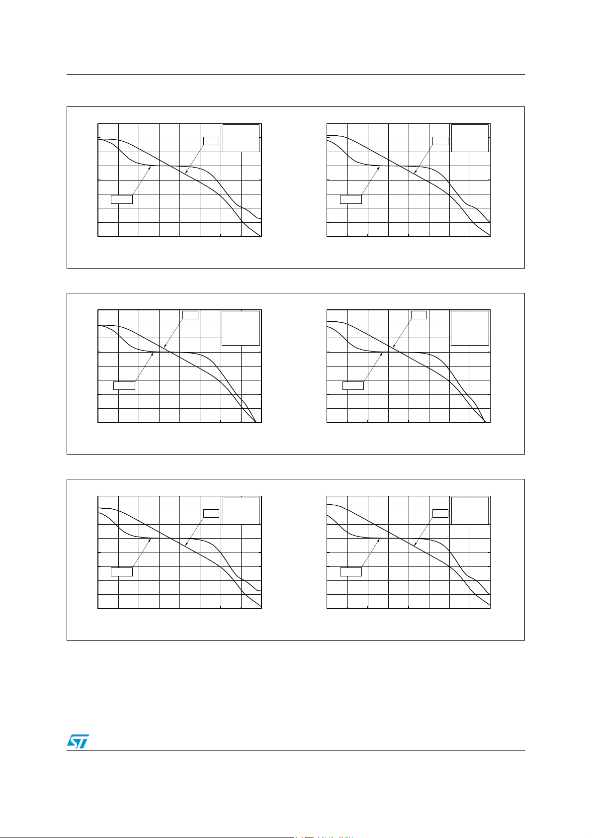
Figure 2. Open-loop frequency response Figure 3. Open-loop frequency response
Gain (dB)
125
100
-25
-50
-75
Ω
=25°C
225
180
135
90
45
0
Vcc=2.5V
RL=16
gain
T
75
AMB
50
25
0
phase
-45
-90
0
10
2
10
4
10
6
10
-135
8
10
Frequency (Hz)
125
100
75
gain
Vcc=5V
RL=16
T
AMB
50
25
Gain (dB)
Phase (°)
0
phase
-25
-50
-75
0
10
2
10
4
10
6
10
Ω
=25°C
225
180
135
90
45
0
-45
-90
-135
8
10
Frequency (Hz)
Figure 4. Open-loop frequency response Figure 5. Open-loop frequency response
125
100
75
gain
Vcc=2.5V
RL=16
CL=400pF
T
AMB
50
25
Gain (dB)
0
phase
-25
-50
-75
0
10
2
10
4
10
6
10
Ω
=25°C
225
180
135
90
45
0
-45
-90
-135
8
10
Frequency (Hz)
125
100
75
gain
Vcc=5V
RL=16
CL=400pF
T
AMB
50
25
Gain (dB)
Phase (°)
0
phase
-25
-50
-75
0
10
2
10
4
10
6
10
Ω
=25°C
225
180
135
90
45
0
-45
-90
-135
8
10
Frequency (Hz)
Phase (°)
Phase (°)
Figure 6. Open-loop frequency response Figure 7. Open-loop frequency response
125
100
75
gain
Vcc=2.5V
RL=32
T
AMB
50
25
Gain (dB)
0
phase
-25
-50
-75
0
10
2
10
4
10
6
10
Ω
=25°C
225
180
135
90
45
0
-45
-90
-135
8
10
Frequency (Hz)
Doc ID 11971 Rev 5 9/32
125
100
75
gain
Vcc=5V
RL=32
T
AMB
50
25
Gain (dB)
Phase (°)
0
phase
-25
-50
-75
0
10
2
10
4
10
6
10
Ω
=25°C
225
180
135
90
45
0
-45
-90
-135
8
10
Frequency (Hz)
Phase (°)

Electrical characteristics TS488-TS489
Figure 8. Open-loop frequency response Figure 9. Open-loop frequency response
125
100
75
gain
Vcc=2.5V
RL=32
CL=400pF
T
AMB
50
25
Gain (dB)
0
phase
-25
-50
-75
0
10
2
10
4
10
Frequency (Hz)
6
10
Ω
=25°C
225
180
135
90
45
0
-45
-90
-135
8
10
125
100
75
gain
Vcc=5V
RL=32
CL=400pF
T
AMB
50
25
Gain (dB)
Phase (°)
0
phase
-25
-50
-75
0
10
2
10
4
10
Frequency (Hz)
6
10
Ω
=25°C
225
180
135
90
45
0
-45
-90
-135
8
10
Figure 10. Open-loop frequency response Figure 11. Open-loop frequency response
125
100
75
gain
Vcc=2.5V
RL=600
T
AMB
50
25
Gain (dB)
0
phase
-25
-50
-75
0
10
2
10
4
10
Frequency (Hz)
6
10
Ω
=25°C
225
180
135
90
45
0
-45
-90
-135
8
10
125
100
75
gain
Vcc=5V
RL=600
T
AMB
50
25
Gain (dB)
Phase (°)
0
phase
-25
-50
-75
0
10
2
10
4
10
Frequency (Hz)
6
10
=25°C
225
180
Ω
135
90
45
0
-45
-90
-135
8
10
Phase (°)
Phase (°)
Figure 12. Power derating curves Figure 13. Power derating curves
0.8
0.6
4-layer PCB
0.4
0.2
No Heat sink
Package Power Dissipation (W)
0.0
0 25 50 75 100 125 150
Ambiant Temperature (°C)
10/32 Doc ID 11971 Rev 5
MiniSO8
3
4-layer PCB
2
1
Package Power Dissipation (W)
0
0 25 50 75 100 125 150
Ambiant Temperature (°C)
DFN8
No heatsink
 Loading...