

TS4871
OUTPUT RAIL TO RAIL 1W AUDIO POWER AMPLIFIER
WITH STANDBY MODE
■OPERATING FROM V
= 2.5V to 5.5V
CC
■1W RAIL TO RAIL OUTPUT POWER @
Vcc=5V, THD=1%, f=1kHz, with 8
Ω Load
■ULTRA LOW CONSUMPTION IN STANDBY
MODE (10nA)
■75dB PSRR @ 217Hz from 5V to 2.6V
■ULTRA LOW POP & CLICK
■ULTRA LOW DISTORTION (0.1%)
■UNITY GAIN STABLE
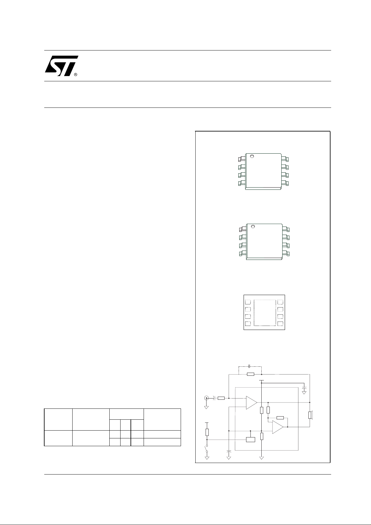
■AVAI LA BL E IN SO8, MiniSO8 & DFN8 3x3mm
DESCRIPTION
The TS487 1 i s an Audio Pow er Amplifier capable
of delivering 1W of continuous RMS Ouput Power
into 8
Ω load @ 5V.
This Audio Am plifier is exhibiting 0.1% distortion
level (THD) from a 5V supply for a Pout = 250mW
RMS. An external standby mode cont rol reduces
the supply current to less than 10n A. An internal
thermal shutdown protection is also provided.
The TS4871 has been designed for high quality
audio applications such as m obile phones and t o
minimize the number of external components.
The unity-gain stable amplifier can be configured
by external gain setting resistors.
PIN CONNECTIONS (Top View)
TS4871IST - MiniSO8
8
7
6
5
8
7
6
5
V
V
8
8
OUT 2
OUT 2
7
7
GND
GND
6
6
Vcc
Vcc
V
V
5
5
IN
VIN-
1
2
3
4
Standby
Bypass
V+
TS4871ID-TS4871IDT - SO8
V+
IN
VIN-
1
2
3
4
Standby
Bypass
TS4871IQT - DFN8
STANDBY
STANDBY
BYPASS
BYPASS
V
V
V
V
1
1
2
2
3
3
IN+
IN+
4
4
IN-
IN-
V2OUT
GND
CC
V
VOUT1
V2OUT
GND
V
VOUT1
OUT 1
OUT 1
CC
APPLICATIONS
■Mobile Phones (Cellular / Cordless)
■Laptop / Notebook Computers
■PDAs
■Portable Audio Devices
ORDER CODE
Part
Number
Temperature
Range: I
TS4871 -40, +85°C
MiniSO & DFN only available in Tape & Reel with T suffix(IST & IQT)
D = Small Outline Package (SO) - also available in Tape & Reel (DT)
June 2003
Package
DSQ
•
••
Marking
4871I
4871
TYPICAL APPLICATION SCHEMATIC
Cfeed
Vcc
Rfeed
6
Audio
Input
Vcc
Rstb
Rin
4
Vin-
Cin
Vin+
3
Bypass
2
Standby
1
Cb
Vcc
-
+
Av=-1
+
Bias
GND
7
Vout1
Vout2
TS4871
Cs
5
RL
8 Ohms
8
1/28
TS4871
ABSOLUTE MAXIMUM RATINGS
Symbol Parameter Value Unit
V
T
T
R
Supply voltage
CC
V
iInput Voltage
Operating Free Air Temperature Range -40 to + 85 °C
oper
Storage Temperature -65 to +150 °C
stg
T
Maximum Junction Temperature 150 °C
j
Thermal Resistance Junction to Ambient
thja
SO8
MiniSO8
QNF8
Pd Power Dissipation
ESD Human Body Model 2 kV
ESD Machine Model 200 V
Latch-up Latch-up Immunity Class A
Lead Temperature (soldering, 10sec) 260 °C
1. All voltages values are measured with respect to the ground pin.
2. The magnitude of input signal must never exceed V
3. Device is protected in case of over temperature by a thermal shutdown active @ 150°C.
4. Exceeding the power derating curves during a long period, involves abnormal operating condition.
1)
2)
3)
6V
GND to V
CC
175
215
70
4)
+ 0.3V / GND - 0.3V
CC
Internally Limited
V
°C/W
OPERATING CONDITIONS
Symbol Parameter Value Unit
V
V
V
R
1. This thermal resistance can be reduced with a suitable PCB layout (see Power Derating Curves Fig. 20)
2. When mounted o n a 4 l ayers PCB
Supply Voltage 2.5 to 5.5 V
CC
to VCC - 1.2V
Common Mode Input Voltage Range
ICM
G
ND
Standby Voltage Input :
≤ V
STB
Device ON
Device OFF
R
Load Resistor 4 - 32
L
Thermal Resistance Junction to Ambient
thja
SO8
1)
MiniSO8
2)
DFN8
G
V
- 0.5V ≤ V
CC
ND
STB
150
190
41
≤ 0.5V
STB
≤ V
CC
V
V
Ω
°C/W
2/28
TS4871
ELECTRICAL CHARACTERISTICS
= +5V, GND = 0V, T
V
CC
Symbol Parameter Min. Typ. Max. Unit
= 25°C (unless otherwise specified)
amb
I
CC
I
STANDBY
Voo
Po
THD + N
PSRR
Φ
GM
GBP
1. Standby mode i s actived when Vstdby is tied to Vcc
2. Dynamic measurements - 20*log(r m s(Vout)/rms(Vripple)). Vripple is the surim posed sinus signal to Vc c @ f = 217Hz
= +3.3V, GND = 0V, T
V
CC
Supply Current
No input signal, no load
Standby Current
1)
No input signal, Vstdby = Vcc, RL = 8
Output Offset Voltage
No input signal, RL = 8
Output Power
THD = 1% Max, f = 1kHz, RL = 8
Total Harmonic Distortion + Noise
Po = 250mW rms, Gv = 2, 20Hz < f < 20kHz, RL = 8
Power Supply Rejection Ratio
f = 217Hz, RL = 8
Phase Margin at Unity Gain
M
R
= 8Ω, CL = 500pF
L
Gain Margin
R
= 8Ω, CL = 500pF
L
Gain Bandwidth Product
R
= 8
Ω
L
amb
Ω
Ω
Ω
Ω
2)
RFeed = 22K
Ω,
Vripple = 200mV rms
Ω,
= 25°C (unless otherwise specified)3)
68mA
10 1000 nA
520mV
1W
0.15 %
75 dB
70 Degrees
20 dB
2MHz
Symbol Parameter Min. Typ. Max. Unit
I
CC
I
STANDBY
Voo
Po
THD + N
PSRR
Φ
GM
GBP
1. Standby mode i s actived when Vstdby is tied to Vcc
2. Dynamic measurements - 20*log(r m s(Vout)/rms(Vripple)). Vripple is the surim posed sinus signal to Vc c @ f = 217Hz
3. All electrical values are made by correlation between 2.6V and 5V measurement s
Supply Current
No input signal, no load
Standby Current
1)
No input signal, Vstdby = Vcc, RL = 8
Output Offset Voltage
No input signal, RL = 8
Output Power
THD = 1% Max, f = 1kHz, RL = 8
Total Harmonic Distortion + Noise
Po = 250mW rms, Gv = 2, 20Hz < f < 20kHz, RL = 8
Power Supply Rejection Ratio
f = 217Hz, RL = 8
Phase Margin at Unity Gain
M
R
= 8Ω, CL = 500pF
L
Gain Margin
R
= 8Ω, CL = 500pF
L
Gain Bandwidth Product
R
= 8
Ω
L
Ω
2)
RFeed = 22K
Ω,
Ω
Ω
Vripple = 200mV rms
Ω,
5.5 8 mA
10 1000 nA
520mV
450 mW
Ω
0.15 %
75 dB
70 Degrees
20 dB
2MHz
3/28

TS4871
ELECTRICAL CHARACTERISTICS
= 2.6V, GND = 0V, T
V
CC
Symbol Parameter Min. Typ. Max. Unit
= 25°C (unless otherwise specified)
amb
I
CC
I
STANDBY
Voo
Po
THD + N
PSRR
Φ
GM
GBP
1. Standby mode i s actived when Vstdby is tied to Vcc
2. Dynamic measurements - 20*log(r m s(Vout)/rms(Vripple)). Vripple is the surim posed sinus signal to Vc c @ f = 217Hz
Supply Current
No input signal, no load
Standby Current
1)
No input signal, Vstdby = Vcc, RL = 8
Output Offset Voltage
No input signal, RL = 8
Output Power
THD = 1% Max, f = 1kHz, RL = 8
Total Harmonic Distortion + Noise
Po = 200mW rms, Gv = 2, 20Hz < f < 20kHz, RL = 8
Power Supply Rejection Ratio
f = 217Hz, RL = 8
Phase Margin at Unity Gain
M
R
= 8Ω, CL = 500pF
L
Gain Margin
R
= 8Ω, CL = 500pF
L
Gain Bandwidth Product
R
= 8
Ω
L
Ω
2)
RFeed = 22K
Ω,
Ω
Ω
Vripple = 200mV rms
Ω,
5.5 8 mA
10 1000 nA
520mV
260 mW
Ω
0.15 %
75 dB
70 Degrees
20 dB
2MHz
Components Functional Description
Rin
Inverting input resistor which sets the closed loop gain in conjunction with Rfeed. This resistor also
forms a high pass filter with Cin (fc = 1 / (2 x Pi x Rin x Cin))
Cin Input coupling capacitor which blocks the DC voltage at the amplifier input terminal
Rfeed Feed back resistor which sets the closed loop gain in conjunction with Rin
Cs Supply Bypass capacitor which provides power supply filtering
Cb Bypass pin capacitor which provides half supply filtering
Cfeed
Low pass filter capacitor allowing to cut the high frequency
(low pass filter cut-off frequency 1 / (2 x Pi x Rfeed x Cfeed))
Rstb Pull-up resistor which fixes the right supply level on the standby pin
Gv Closed loop gain in BTL configuration = 2 x (Rfeed / Rin)
REMARKS
1. All measurements, except PSRR measurements, are made with a supply bypass capacitor Cs = 100µF.
2. External resistors are not needed for having better stability when supply @ Vcc down to 3V. By the way,
the quiescent current remains the same.
3. The standby response time is about 1µs.
4/28
TS4871
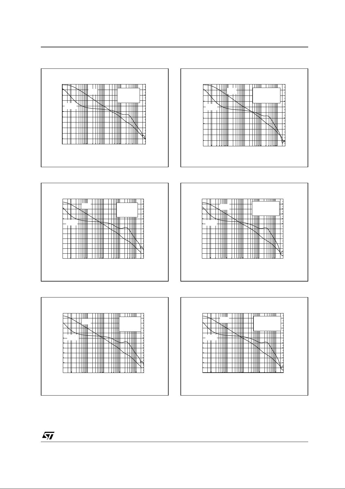
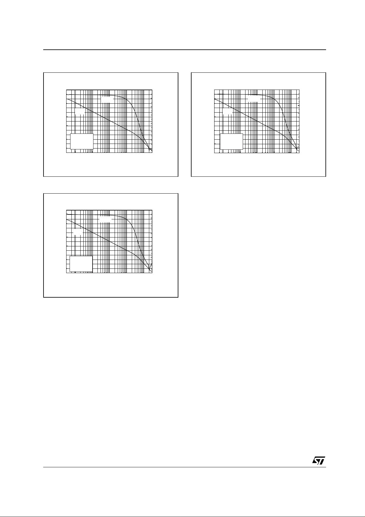
Fig. 1 : Open Loop Frequency Response
0
60
40
Phase
20
Gain (dB)
0
-20
-40
0.3 1 10 100 1000 10000
Gain
Frequency (kHz)
Vcc = 5V
RL = 8
Tamb = 25°C
Ω
-20
-40
-60
-80
-100
-120
-140
-160
-180
-200
-220
Fig. 3 : Open Loop Frequency Response
80
60
40
20
Gain (dB)
0
-20
-40
0.3 1 10 100 1000 10000
Gain
Phase
Frequency (kHz)
Vcc = 3.3V
RL = 8
Ω
Tamb = 25°C
0
-20
-40
-60
-80
-100
-120
-140
-160
-180
-200
-220
-240
Phase (Deg)
Phase (Deg)
Fig. 2 : Open Loop Frequency Response
0
60
40
Phase
20
Gain (dB)
0
-20
-40
0.3 1 10 100 1000 10000
Gain
Frequency (kHz)
Vcc = 5V
ZL = 8Ω + 560pF
Tamb = 25°C
-20
-40
-60
-80
-100
-120
-140
-160
-180
-200
-220
Fig. 4 : Open Loop Frequency Response
80
60
40
20
Gain (dB)
0
-20
-40
0.3 1 10 100 1000 10000
Gain
Phase
Frequency (kHz)
Vcc = 3.3V
ZL = 8Ω + 560pF
Tamb = 25°C
0
-20
-40
-60
-80
-100
-120
-140
-160
-180
-200
-220
-240
Phase (Deg)
Phase (Deg)
Fig. 5 : Open Loop Frequency Response
80
Vcc = 2.6V
RL = 8
Tamb = 25°C
Phase
Gain
Frequency (kHz)
60
40
20
Gain (dB)
0
-20
-40
0.3 1 10 100 1000 10000
0
-20
-40
Ω
-60
-80
-100
-120
-140
-160
Phase (Deg)
-180
-200
-220
-240
Fig. 6 : Open Loop Frequency Response
80
Vcc = 2.6V
ZL = 8Ω + 560pF
Tamb = 25°C
60
40
20
Gain (dB)
0
-20
-40
0.3 1 10 100 1000 10000
Gain
Phase
Frequency (kHz)
0
-20
-40
-60
-80
-100
-120
-140
-160
-180
-200
-220
-240
Phase (Deg)
5/28
TS4871
0.3 1 10 100 1000 10000
-40
-20
0
20
40
60
80
100
-240
-220
-200
-180
-160
-140
-120
-100
-80
Gain (dB)
Frequency (kHz)
Vcc = 3.3V
CL = 560pF
Tamb = 25°C
Gain
Phase
Phase (Deg)
Fig. 7 : Open Loop Frequency Response
100
80
60
Gain
40
20
Gain (dB)
0
Vcc = 5V
CL = 560pF
-20
Tamb = 25°C
-40
0.3 1 10 100 1000 10000
Phase
Frequency (kHz)
-80
-100
-120
-140
-160
-180
-200
-220
Phase (Deg)
Fig. 9 : Open Loop Frequency Response
100
80
60
Gain
40
20
Gain (dB)
0
Vcc = 2.6V
-20
CL = 560pF
Tamb = 25°C
-40
0.3 1 10 100 1000 10000
Phase
Frequency (kHz)
-80
-100
-120
-140
-160
-180
-200
-220
-240
Phase (Deg)
Fig. 8 : Open Loop Frequency Response
6/28
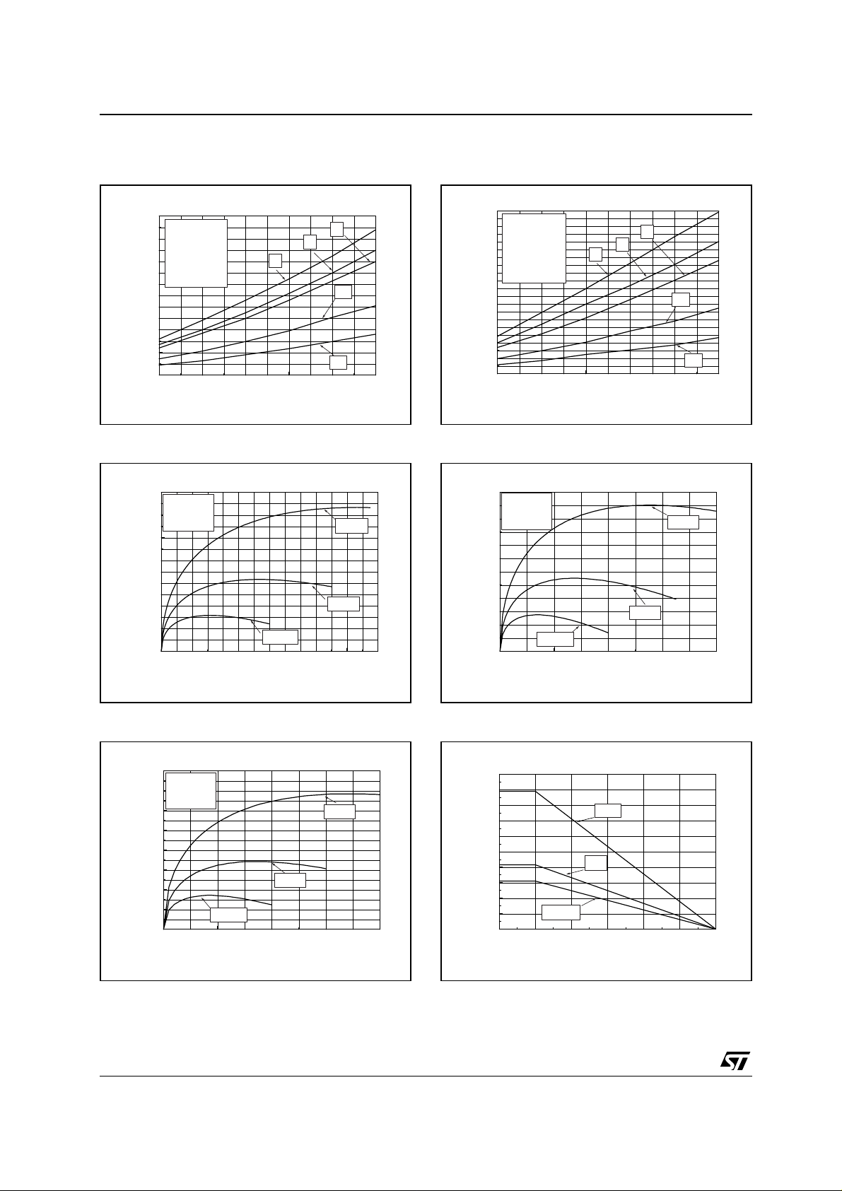
TS4871
10 100 1000 10000 100000
-60
-50
-40
-30
-20
-10
Vcc = 5, 3.3 & 2.6V
Rfeed = 22kΩ, Rin = 22k
Cb = 1µF
Rg = 100Ω, RL = 8Ω
Tamb = 25°C
Cin=22nF
Cin=100nF
Cin=220nF
Cin=330nF
Cin=1µF
PSRR (dB)
Frequency (Hz)
Fig. 10 : Power Supply Rejection Ratio (PSRR)
vs Power supply
-30
Vripple = 200mVrms
Rfeed = 22
-40
-50
PSRR (dB)
-60
-70
-80
10 100 1000 10000 100000
Ω
Input = floating
RL = 8
Ω
Tamb = 25°C
Vcc = 5V, 3.3V & 2.6V
Cb = 1µF & 0.1µF
Frequency (Hz)
Fig. 12 : Power Supply Rejection Ratio (PSRR)
vs Bypass Capacitor
-10
-20
-30
-40
-50
PSRR (dB)
-60
-70
-80
10 100 1000 10000 100000
Cb=100µF
Cb=1µF
Cb=10µF
Vcc = 5, 3.3 & 2.6V
Rfeed = 22k
Rin = 22k, Cin = 1µF
Rg = 100Ω, RL = 8Ω
Tamb = 25°C
Cb=47µF
Frequency (Hz)
Fig. 11 : Power Supply Rejectio n Ratio (PSRR)
vs Feedback Capacitor
-10
Vcc = 5, 3.3 & 2.6V
-20
Cb = 1µF & 0.1µF
Rfeed = 22k
-30
Vripple = 200mVrms
Input = floating
-40
RL = 8
Tamb = 25°C
-50
PSRR (dB)
-60
-70
-80
10 100 1000 10000 100000
Ω
Ω
Frequency (Hz)
Cfeed=0
Cfeed=150pF
Cfeed=330pF
Cfeed=680pF
Fig. 13 : Power Supply Rejectio n Ratio (PSRR)
vs Input Capacitor
Fig. 14 : Power Supply Rejection Ratio (PSRR)
vs Feedback Resistor
-10
Vcc = 5, 3.3 & 2.6V
-20
Cb = 1µF & 0.1µF
Vripple = 200mVrms
-30
Input = floating
RL = 8Ω
-40
Tamb = 25°C
-50
PSRR (dB)
-60
-70
-80
10 100 1000 10000 100000
Rfeed=110kΩ
Rfeed=47kΩ
Rfeed=22kΩ
Rfeed=10kΩ
Frequency (Hz)
7/28
TS4871
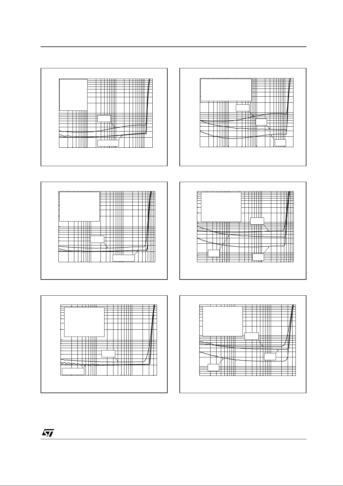
2.5 3.0 3.5 4.0 4.5 5.0
0.0
0.2
0.4
0.6
0.8
1.0
1.2
1.4
1.6
1.8
2.0
4Ω
6Ω
8Ω
16Ω
32Ω
Gv = 2 & 10
Cb = 1µF
F = 1kHz
BW < 125kHz
Tamb = 25°C
Output power @ 10% THD + N (W)
Vcc (V)
0.0 0.2 0.4 0.6 0.8
0.0
0.1
0.2
0.3
0.4
0.5
0.6
RL=4
Ω
RL=8
Ω
Vcc=3.3V
F=1kHz
THD+N<1%
RL=16
Ω
Power Dissipation (W)
Output Power (W)
0 25 50 75 100 125 150
0.0
0.2
0.4
0.6
0.8
1.0
1.2
1.4
1.6
1.8
2.0
SO8
MiniSO8
QFN8
Power Dissipation (W)
Ambiant Temperature (°C)
Fig. 15 : Pout @ THD + N = 1% vs Supply
Voltage vs RL
1.4
Gv = 2 & 10
1.2
Cb = 1µF
F = 1kHz
1.0
BW < 125kHz
Tamb = 25°C
0.8
0.6
0.4
0.2
Output power @ 1% THD + N (W)
0.0
2.5 3.0 3.5 4.0 4.5 5.0
4
Vcc (V)
Ω
8
Ω
6
Ω
16
Ω
32
Ω
Fig. 17 : Power Dissipation vs Pout
1.4
Vcc=5V
F=1kHz
1.2
THD+N<1%
1.0
0.8
0.6
Power Dissipation (W)
0.4
0.2
0.0
0.0 0.2 0.4 0.6 0.8 1.0 1.2 1.4
RL=16
Ω
Output Power (W)
RL=4
RL=8
Ω
Ω
Fig. 16 : Pout @ THD + N = 10% vs Supply
Voltage vs RL
Fig. 18 : Power Dissipation vs Pout
Fig. 19 : Power Dissipation vs Pout
0.40
Vcc=2.6V
0.35
F=1kHz
THD+N<1%
0.30
0.25
0.20
0.15
Power Dissipation (W)
0.10
0.05
0.00
0.0 0.1 0.2 0.3 0.4
8/28
RL=16
RL=8
Ω
Output Power (W)
Fig. 20 : Power Derating Curves
RL=4
Ω
Ω
TS4871
1E-3 0.01 0.1 1
0.1
1
10
RL = 4Ω, Vcc = 3.3V
Gv = 10
Cb = Cin = 1µF
BW < 125kHz
Tamb = 25°C
20kHz
20Hz
1kHz
THD + N (%)
Output Power (W)
1E-3 0.01 0.1
0.1
1
10
RL = 4Ω, Vcc = 2.6V
Gv = 10
Cb = Cin = 1µF
BW < 125kHz
Tamb = 25°C
20kHz
20Hz
1kHz
THD + N (%)
Output Power (W)
Fig. 21 : THD + N vs Output Power
10
Rl = 4
Ω
Vcc = 5V
Gv = 2
Cb = Cin = 1µF
BW < 125kHz
Tamb = 25°C
1
THD + N (%)
0.1
1E-3 0.01 0.1 1
20kHz
20Hz, 1kHz
Output Power (W)
Fig. 23 : THD + N vs Output Power
10
RL = 4Ω, Vcc = 3.3V
Gv = 2
Cb = Cin = 1µF
BW < 125kHz
Tamb = 25°C
1
THD + N (%)
20kHz
Fig. 22 : THD + N vs Output Power
10
RL = 4Ω, Vcc = 5V
Gv = 10
Cb = Cin = 1µF
BW < 125kHz, Tamb = 25°C
1
THD + N (%)
0.1
1E-3 0.01 0.1 1
20kHz
20Hz
Output Power (W)
Fig. 24 : THD + N vs Output Power
1kHz
0.1
1E-3 0.01 0.1 1
Output Power (W)
Fig. 25 : THD + N vs Output Power
10
RL = 4Ω, Vcc = 2.6V
Gv = 2
Cb = Cin = 1µF
BW < 125kHz
Tamb = 25°C
1
THD + N (%)
20Hz, 1kHz
0.1
1E-3 0.01 0.1
Output Power (W)
20Hz, 1kHz
Fig. 26 : THD + N vs Output Power
20kHz
9/28
 Loading...