

TS472
Very low noise microphone preamplifier with
2.0 V bias output and active low standby mode
Features
■ Low noise: 10 nV/√Hz typ. equivalent input
noise at F = 1 kHz
■ Fully-differential input/output
■ 2.2 to 5.5 V single supply operation
■ Low power consumption at 20 dB: 1.8 mA
■ Fast start up time at 0 dB: 5 ms typ.
■ Low distortion: 0.1% typ.
■ 40 kHz bandwidth regardless of the gain
■ Active low standby mode function (1 μA max)
■ Low noise 2.0 V microphone bias output
■ Available in flip-chip lead-free package and in
QFN24 4 x 4 mm package
■ ESD protection (2 kV)
Applications
■ Video and photo cameras with sound input
■ Sound acquisition and voice recognition
■ Video conference systems
■ Notebook computers and PDAs
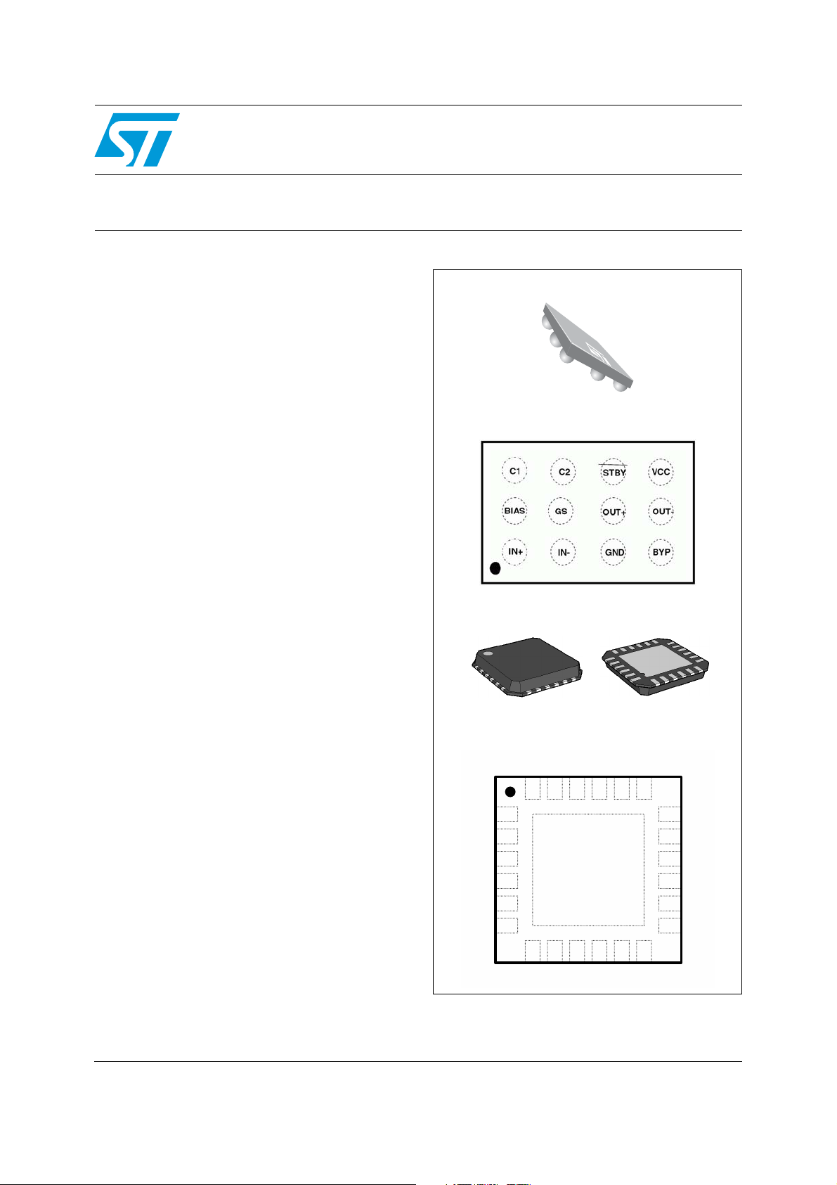
Flip-chip - 12 bumps
Pin connections (top view)
QFN24
Description
Pin connections (top view)
The TS472 is a differential-input microphone
GND STBY VCC
preamplifier optimized for high-performance PDA
and notebook audio systems.
This device features an adjustable gain from 0 to
40 dB with excellent power-supply and commonmode rejection ratios. In addition, the TS472 has
a very low noise microphone bias generator of
2V.
It also includes a complete shutdown function,
with active low standby mode.
August 2009 Doc ID 11015 Rev 6 1/25
BYP
GND
1
NC
2
3
NC
4
5
IN-
6
NC
8 9 10 11 12
7
IN+ GS BIAS
NC NC NC
NCNCNC
192021222324
18
NC
OUT+
17
OUT-
16
C2
15
14
C1
13
NC
www.st.com
25

Contents TS472
Contents
1 Typical application schematic . . . . . . . . . . . . . . . . . . . . . . . . . . . . . . . . . 3
2 Absolute maximum ratings . . . . . . . . . . . . . . . . . . . . . . . . . . . . . . . . . . . 5
3 Electrical characteristics . . . . . . . . . . . . . . . . . . . . . . . . . . . . . . . . . . . . . 6
4 Application information . . . . . . . . . . . . . . . . . . . . . . . . . . . . . . . . . . . . . 13
4.1 Differential configuration principle . . . . . . . . . . . . . . . . . . . . . . . . . . . . . . 13
4.2 Higher cut-off frequency . . . . . . . . . . . . . . . . . . . . . . . . . . . . . . . . . . . . . . 13
4.3 Lower cut-off frequency . . . . . . . . . . . . . . . . . . . . . . . . . . . . . . . . . . . . . . 14
4.4 Low-noise microphone bias source . . . . . . . . . . . . . . . . . . . . . . . . . . . . . 14
4.5 Gain settings . . . . . . . . . . . . . . . . . . . . . . . . . . . . . . . . . . . . . . . . . . . . . . 15
4.6 Wake-up time . . . . . . . . . . . . . . . . . . . . . . . . . . . . . . . . . . . . . . . . . . . . . . 16
4.7 Standby mode . . . . . . . . . . . . . . . . . . . . . . . . . . . . . . . . . . . . . . . . . . . . . 17
4.8 Layout considerations . . . . . . . . . . . . . . . . . . . . . . . . . . . . . . . . . . . . . . . . 17
4.9 Single-ended input configuration . . . . . . . . . . . . . . . . . . . . . . . . . . . . . . . 17
4.10 Demonstration board . . . . . . . . . . . . . . . . . . . . . . . . . . . . . . . . . . . . . . . . 18
5 Package information . . . . . . . . . . . . . . . . . . . . . . . . . . . . . . . . . . . . . . . . 19
5.1 Flip-chip package information . . . . . . . . . . . . . . . . . . . . . . . . . . . . . . . . . 19
5.2 QFN24 package information . . . . . . . . . . . . . . . . . . . . . . . . . . . . . . . . . . 21
6 Ordering information . . . . . . . . . . . . . . . . . . . . . . . . . . . . . . . . . . . . . . . 23
7 Revision history . . . . . . . . . . . . . . . . . . . . . . . . . . . . . . . . . . . . . . . . . . . 24
2/25 Doc ID 11015 Rev 6
TS472 Typical application schematic
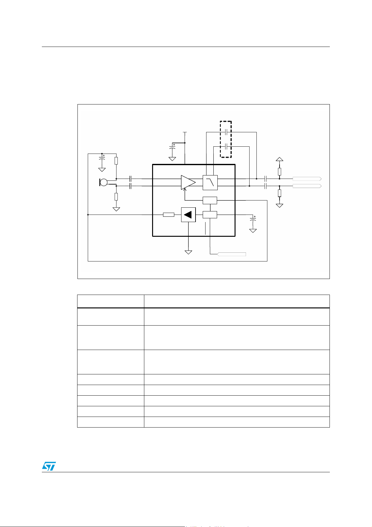
1 Typical application schematic
Figure 1 shows a typical application schematic for the TS472.
Figure 1. Application schematic (flip-chip)
Optional
VCC
C1
Cs
1uF
C3
Rpos
1uF
Cin+
+
Electret Mic
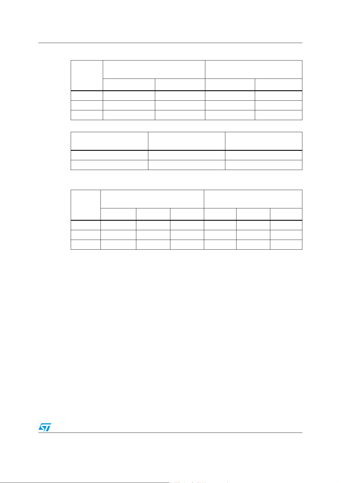
Table 1. Description of external components
Cin-
Rneg
U1 TS472_FC
Vcc
IN+
IN-
BIAS
2.0V
GND
C1
G
Bias
STDBY
C2
GAIN
SELECT
BYPASS
Standby Control
C2
OUT+
OUT-
Components Functional description
C
, C
in+
in-
Input coupling capacitors that block the DC voltage at the amplifier input
terminal.
Output coupling capacitors that block the DC voltage coming from the
, C
C
out+
out-
amplifier output terminal (pins C2 and D2) and determine the lower cut-off
frequency (see Section 4.3: Lower cut-off frequency).
Output load resistors used to charge the output coupling capacitors C
, R
R
out+
out-
These output resistors can be represented by an input impedance of a
following stage.
, R
R
pos
neg
C
s
C
b
, C
C
1
2
C
3
Polarizing resistors for biasing of a microphone.
Supply bypass capacitor that provides power supply filtering.
Bypass pin capacitor that provides half-supply filtering.
Low pass filter capacitors allowing to cut the high frequency.
Bias output filtering capacitor.
Cb
1uF
Cout+
Cout-
Rout+
Rout-
Positive Output
Negative Output
out
.
Doc ID 11015 Rev 6 3/25
Typical application schematic TS472
Table 2. Pin descriptions
Pin name
IN+ A1 8 Positive differential input
IN- B1 5 Negative differential input
BIAS A2 10 2 V bias output
GND C1 4, 22 Ground
STBY C3 21 Standby
BYP D1 2 Bypass
GS B2 9 Gain select
OUT- D2 16 Negative differential output
OUT+ C2 17 Positive differential output
C1 A3 14 Low-pass filter capacitor
C2 B3 15 Low-pass filter capacitor
Vcc D3 20 Power supply
NC ---
Flip-chip
designator
QFN
designator
3, 6, 7, 11,
12, 13, 18,
19, 23, 24
Not connected, floating pins
Pin description
4/25 Doc ID 11015 Rev 6
TS472 Absolute maximum ratings
2 Absolute maximum ratings
Table 3. Absolute maximum ratings
Symbol Parameter Value Unit
V
T
T
CC
V
oper
stg
T
Supply voltage
Input voltage -0.3 to VCC+0.3 V
i
Operating free air temperature range -40 to + 85 °C
Storage temperature -65 to +150 °C
Maximum junction temperature 150 °C
j
Thermal resistance junction to ambient:
R
thja
Flip-chip
QFN24
ESD Human body model 2 kV
ESD Machine model 200 V
Lead temperature (soldering, 10sec) 250 °C
1. All voltage values are measured with respect to the ground pin.
Table 4. Operating conditions
(1)
6V
180
110
°C/W
Symbol Parameter Value Unit
V
CC
A
Supply voltage 2.2 to 5.5 V
Typical differential gain
(GS connected to 4.7 kΩ or bias)
20 dB
Standby voltage input:
V
R
STBY
T
op
thja
Device ON
Device OFF
1.5 ≤ V
GND ≤ V
STBY
STBY
≤ V
CC
≤ 0.4
Operational free air temperature range -40 to +85 °C
Thermal resistance junction to ambient:
Flip-chip
QFN24
150
60
V
°C/W
Doc ID 11015 Rev 6 5/25
Electrical characteristics TS472
3 Electrical characteristics
Table 5. Electrical characteristics at VCC = 3 V with GND = 0 V, T
(unless otherwise specified)
Symbol Parameter Min. Typ. Max. Unit
amb
= 25° C
e
THD+N
V
Equivalent input noise voltage density
n
=100Ω at 1 kHz
R
EQ
Total harmonic distortion + noise
20 Hz ≤F ≤ 20 kHz, gain = 20 dB, V
Input voltage, gain = 20 dB 10 70 mV
in
=50mV
in
Bandwidth at -3 dB
B
Bandwidth at -1 dB
W
pin A3, B3 floating
Overall output voltage gain (Rgs variable):
G
Minimum gain, Rgs infinite
Maximum gain, Rgs = 0
Input impedance referred to GND 80 100 120 kΩ
in
Resistive load 10 kΩ
Capacitive load 100 pF
Supply current, gain = 20 dB 1.8 2.4 mA
Standby current 1 μA
R
LOAD
C
LOAD
I
I
STBY
Z
CC
Power supply rejection ratio, gain = 20 dB,
PSRR
F = 217 Hz, V
Differential output
= 200 mVpp, inputs grounded
ripple
Single-ended outputs,
Table 6. Bias output: VCC = 3 V, GND = 0 V, T
(unless otherwise specified)
RMS
amb
39.5
= 25° C
-3
nV
10
------------
0.1 %
40
20 kHz
-1.5
dB
41042.5
-70
dB
-46
Hz
RMS
Symbol Parameter Min. Typ. Max. Unit
V
R
I
out
PSRR
No load condition 1.9 2 2.1 V
out
Output resistance 80 100 120 W
out
Output bias current 2 mA
Power supply rejection ratio, F = 217 Hz,
= 200 mVpp
V
ripple
6/25 Doc ID 11015 Rev 6
70 80 dB
TS472 Electrical characteristics
Table 7. Differential RMS noise voltage
Gain
Input referred noise voltage
(μV
)
RMS
Output noise voltage
(μV
)
RMS
(dB)
Unweighted filter A-weighted filter Unweighted filter A-weighted filter
015 10 15 10
20 3.4 2.3 34 23
40 1.4 0.9 141 91
Table 8. Bias output RMS noise voltage
(1)
C
3
(μF)
Unweighted filter
RMS
)
(μV
154.4
10 2.2 1.2
1. Bias output filtering capacitor.
Table 9. SNR (signal to noise ratio), THD+N < 0.5%
Unweighted filter 20 Hz - 20 kHz
Gain
(dB)
(dB)
=2.2V VCC=3V VCC=5.5V VCC=2.2V VCC=3V VCC=5.5V
V
CC
0 75 76 76798080
A-weighted filter
(μV
RMS
A-weighted filter
(dB)
)
20 82 83 83 89 90 90
40 70 72 74 80 82 84
Doc ID 11015 Rev 6 7/25
Electrical characteristics TS472
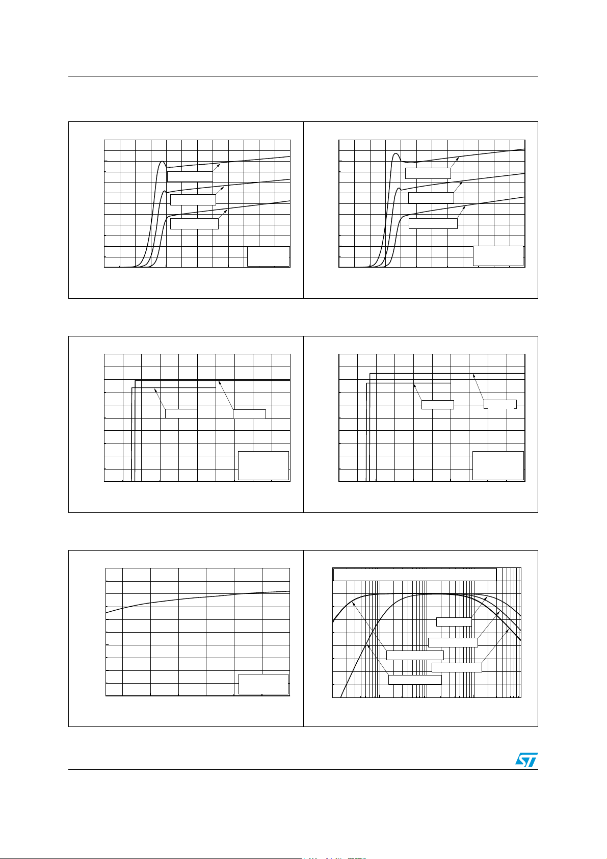
Figure 2. Current consumption vs. power
supply voltage
3.0
2.5
2.0
1.5
1.0
0.5
Current Consumption (mA)
0.0
0123456
Tamb=85°C
Tamb=25°C
Tamb=-40°C
No Loads
GS floating
Power Supply Voltage (V)
Figure 4. Current consumption vs. standby
voltage
2.5
2.0
Figure 3. Current consumption vs. power
supply voltage
3.0
2.5
2.0
1.5
1.0
0.5
Current Consumption (mA)
0.0
0123456
Tamb=85°C
Tamb=25°C
Tamb=-40°C
No Loads
GS grounded
Power Supply Voltage (V)
Figure 5. Current consumption vs. standby
voltage
2.5
2.0
1.5
1.0
0.5
Current Consumption (mA)
0.0
012345
Vcc=3V
Standby Voltage (V)
Vcc=5V
No Loads
GS floating
Tamb = 25°C
Figure 6. Standby threshold voltage vs.
power supply voltage
1.0
0.8
0.6
0.4
0.2
Standby Treshold Voltage (V)
0.0
2.2
345
Power Supply V oltage (V)
No Loads
Tamb = 25°C
1.5
1.0
0.5
Current Consumption (mA)
0.0
012345
Standby Voltage (V)
Figure 7. Frequency response
30
5.5
Cb=1μF, T
20
10
PSRR (dB)
0
-10
-20
10 100 1000 10000 100000
=25°C, Gain=20dB, Rout=100k
AMB
Cin,Cout=100nF
Cin,Cout=10nF
Frequency (Hz)
Vcc=3V
no C1,C2
C1,C2=100pF
C1,C2=220pF
Vcc=5V
No Loads
GS grounded
Tamb = 25°C
Ω
8/25 Doc ID 11015 Rev 6
 Loading...