

Features
■ High dynamic features
■ Large output swing (±2.4 V at V
■ Low noise level: 4 nV/√Hz
■ Low distortion: 0.003 %
■ Operating range: 2.7 V to 10 V
■ Available in SOT23-5 micropackage
CC
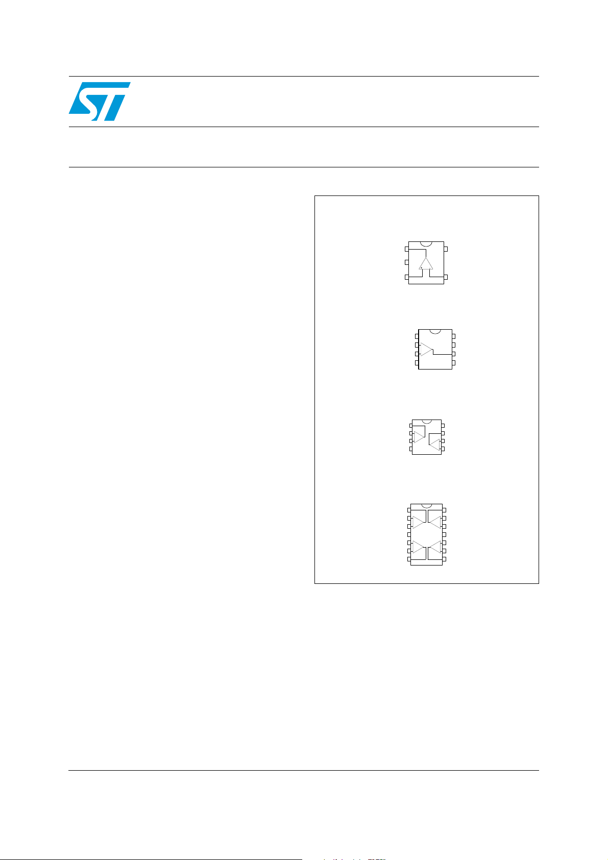
TS461, TS462, TS464
Output rail-to-rail operational amplifiers
TS461CLT
= ±2.5 V)
Output
V
Non-inverting input
1
2
DD
3
TS461CD
V
5
CC
Inverting input
4
Applications
■ Sound cards
■ PDAs
■ CD players
■ Recording equipment
■ Multimedia
■ Microphone pre-amplifiers
Description
The TS461, TS462 and TS464 family of
operational amplifiers can operate with voltages
as low as ±1.35 V and reach a minimum of
±2 Vpp of output swing when supplied with
±2.5 V.
The devices are well-suited to all kinds of portable
and battery-supplied equipment, where low noise
and low distortion are key requirements.
The TS461, TS462 and TS464 offer excellent
output rail-to-rail performances at an attractive
cost.
N.C.
Inverting Input 1
Non-inverting Input 1
1
N.C.
2
-
+
3
V
4
DD
8
V
7
CC
6
Output 2
N.C.
5
TS462CD-TS462CPT-TS462CST
Output 1
Inverting Input 1
Non-inverting Input 1
1
-
2
+
3
V
45
DD
8
7
-
6
+
V
CC
Output 2
Inverting Input 2
Non-inverting Input 2
TS464CD-TS464CPT
14
Output 1
Inverting Input 1
Non-inverting Input 1
Non-inverting Input 2
Inverting Input 2
Output 2
1
2
-
+
3
V
4
CC
5
+
-
6
7
-
+
+
-
Output 4
13
Inverting Input 4
12
Non-inverting Input 4
11
V
DD
10
Non-inverting Input 3
9
Inverting Input 3
8
Output 3
April 2009 Rev 3 1/13
www.st.com
13
Absolute maximum ratings and operating conditions TS461, TS462, TS464
1 Absolute maximum ratings and operating conditions
Table 1. Key parameters and their absolute maximum ratings
Symbol Parameter Value Unit
V
CC
V
id
V
in
T
oper
T
std
T
R
thja
ESD
Supply voltage
Differential Input Voltage
Input voltage range V
Operating free air temperature range -20 to +70 °C
Storage temperature range -65 to +150 °C
Maximum junction temperature 150 °C
j
Thermal resistance junction to case
SOT23-5
SO8
SO14
TSSOP8
TSSOP14
HBM: human body model
MM: machine model
(1)
(5)
(2)
(4)
(3)
12 V
±V
CC
-0.3 to VCC+0.3 V
DD
250
125
103
120
100
2kV
200 V
V
°C/W
CDM: charged device model 1.5 kV
Lead temperature (soldering, 10 sec) 250 °C
1. All voltages values, except differential voltage are with respect to network group terminal.
2. Differential voltages are non-inverting input terminal with respect to the inverting input terminal.
3. Short-circuits can cause excessive heating and destructive dissipation.
4. Human body model: 100 pF discharged through a 1.5 kΩ resistor into pin of device.
5. Machine model ESD: a 200 pF capacitor is charged to the specified voltage, then discharged directly into
the IC with no external series resistor (internal resistor < 5 Ω), into pin-to-pin of device.
Table 2. Operating conditions
Symbol Parameter Value Unit
V
Vicm Common mode input voltage range
T
oper
Supply voltage 2.7 to 10 V
CC
+1.15 to
V
DD
VCC - 1.15
Operating free air temperature range -20 to +70 °C
V
2/13
TS461, TS462, TS464 Electrical characteristics
2 Electrical characteristics
Table 3. VCC = 2.5 V, VDD = -2.5 V, V
T
= 25° C (unless otherwise specified)
amb
Symbol Parameter Min. Typ. Max. Unit
= VCC / 2, RL connected to VCC / 2,
icm
V
io
ΔV
I
io
I
ib
CMR
SVR
A
vd
V
OH
V
OL
I
CC
GBP
SR
en
THD
Input offset voltage
≤ T
T
min.
Input offset voltage drift 5 μV/°C
io
amb
≤ T
max.
Input offset current
T
min.
≤ T
amb
≤ T
max.
Input bias current
≤ T
T
min.
amb
≤ T
max.
15
10 150
200
200
Common mode rejection ratio
= ±1.35 V 60 85
V
icm
Supply voltage rejection ratio
V
= ±2 V to ±3 V 60 70
CC
Large signal voltage gain
= 2 kΩ
R
L
High level output voltage
= 2 kΩ
R
L
Low level output voltage
= 2 kΩ
R
L
70 80 dB
22.4 V
-2.4 -2 V
Supply current, per amplifier
Unity gain - no load 2 2.8
Gain bandwidth product
f = 100 kHz, RL = 2 kΩ, CL = 100 pF 8.5 12
Slew rate
A
= 1, Vin = ±1 V 2.8 4
V
Equivalent input noise voltage
f = 100 kHz 4
Total harmonic distortion
f = 1 kHz, A
= -1, RL = 10 kΩ 0.003
V
7
200
750
1000
mV
nA
nA
dB
dB
mA
MHz
V/μs
nV
-----------Hz
%
3/13

Package information TS461, TS462, TS464
3 Package information
In order to meet environmental requirements, ST offers these devices in different grades of
ECOPACK
specifications, grade definitions and product status are available at: www.st.com.
ECOPACK
®
packages, depending on their level of environmental compliance. ECOPACK®
®
is an ST trademark.
4/13
 Loading...