

TS4621E
High-performance class-G stereo headphone amplifier
with I
2
C volume control
Features
■ Power supply range: 2.3 V to 4.8 V
■ 0.6 mA/channel quiescent current
■ 2.1 mA current consumption with
100 µW/channel (10 dB crest factor)
■ 0.006% typical THD+N at 1 kHz
■ 100 dB typical PSRR at 217 Hz
■ 100 dB of SNR A-weighted at G = 0 dB
■ Zero pop and click
2
■ I
C interface for volume control
■ Digital volume control range from -60 dB to
+4 dB
■ Independent right and left channel shutdown
control
■ Integrated high-efficiency buck converter
■ Low software standby current: 5 µA max
■ Output-coupling capacitors removed
■ Thermal shutdown and short-circuit protection
■ Flip-chip package: 1.65 mm x 1.65 mm,
400 µm pitch, 16 bumps
Applications
■ Cellular phones, smart phones
■ Mobile internet devices
■ PMP/MP3 players
Description
The TS4621E is a class-G stereo headphone
driver dedicated to high audio performance, high
power efficiency and space-constrained
applications.
It is based on the core technology of a low power
dissipation amplifier combined with a highefficiency buck converter for supplying this
amplifier.
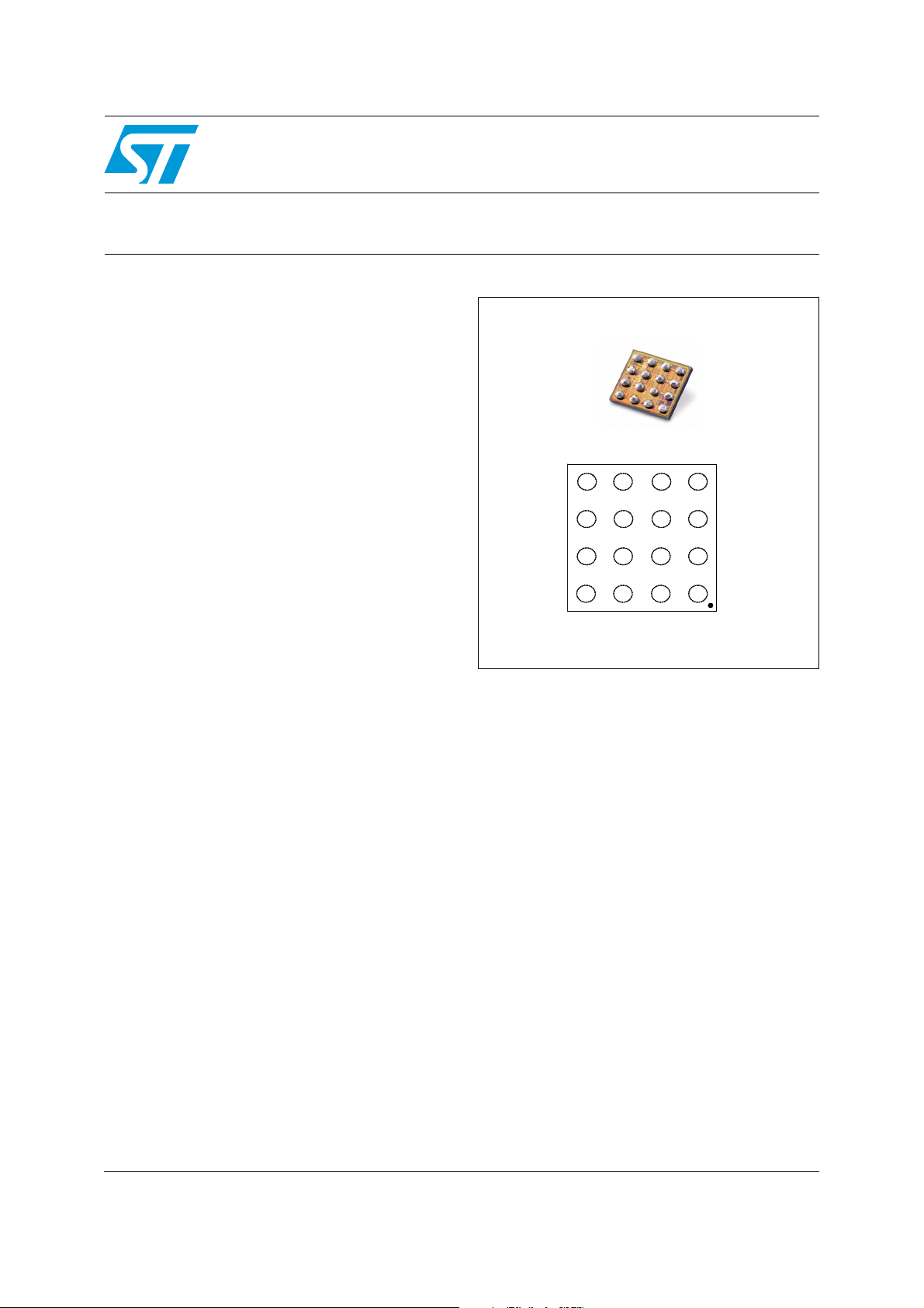
TS4621EIJT - flip-chip
Pinout (top view)
SCL
SCL
SDA
PVSS
PVSS
C1
C1
AVDD
AVDD
SDA
C2
C2
AGND
AGND
SW
SW
D
D
C
C
B
B
A
A
INR-
INR-
VOUTR
VOUTR
INR+
INR+
CMS
CMS
HPVDD
INL+
HPVDD
INL+
VOUTL
VOUTL
INL-
INL-
4321
4321
Balls are underneath
When powered by a battery, the buck converter
generates the appropriate voltage to the amplifier
depending on the amplitude of the audio signal to
supply the headsets. It achieves a total 2.1 mA
current consumption at 100 µW output power
(10 dB crest factor).
THD+N is 0.02% maximum at 1 kHz and PSRR is
100 dB at 217 Hz, which ensures a high audio
quality of the device in a wide range of
environments.
The traditionally bulky output coupling capacitors
can be removed.
A dedicated common-mode sense pin removes
parasitic ground noise.
The TS4621E is designed to be used with an
output serial resistor. It ensures unconditional
stability over a wide range of capacitive loads.
The TS4621E is packaged in a tiny 16-bump
flip-chip package with a pitch of 400 µm.
September 2011 Doc ID 022201 Rev 1 1/32
www.st.com
32

Contents TS4621E
Contents
1 Absolute maximum ratings and operating conditions . . . . . . . . . . . . . 3
2 Typical application schematics . . . . . . . . . . . . . . . . . . . . . . . . . . . . . . . . 5
3 Electrical characteristics . . . . . . . . . . . . . . . . . . . . . . . . . . . . . . . . . . . . . 7
4 Application information . . . . . . . . . . . . . . . . . . . . . . . . . . . . . . . . . . . . . 22
4.1 I2C bus interface . . . . . . . . . . . . . . . . . . . . . . . . . . . . . . . . . . . . . . . . . . . . 22
4.1.1 I²C bus operation . . . . . . . . . . . . . . . . . . . . . . . . . . . . . . . . . . . . . . . . . . 22
4.1.2 Control register CR2 - address 2 . . . . . . . . . . . . . . . . . . . . . . . . . . . . . . 24
4.1.3 Control register CR1 - address 1 . . . . . . . . . . . . . . . . . . . . . . . . . . . . . . 25
4.2 Wake-up and standby time definition . . . . . . . . . . . . . . . . . . . . . . . . . . . . 26
4.3 Common mode sense . . . . . . . . . . . . . . . . . . . . . . . . . . . . . . . . . . . . . . . 27
5 Package information . . . . . . . . . . . . . . . . . . . . . . . . . . . . . . . . . . . . . . . . 28
6 Ordering information . . . . . . . . . . . . . . . . . . . . . . . . . . . . . . . . . . . . . . . 30
7 Revision history . . . . . . . . . . . . . . . . . . . . . . . . . . . . . . . . . . . . . . . . . . . 31
2/32 Doc ID 022201 Rev 1
TS4621E Absolute maximum ratings and operating conditions
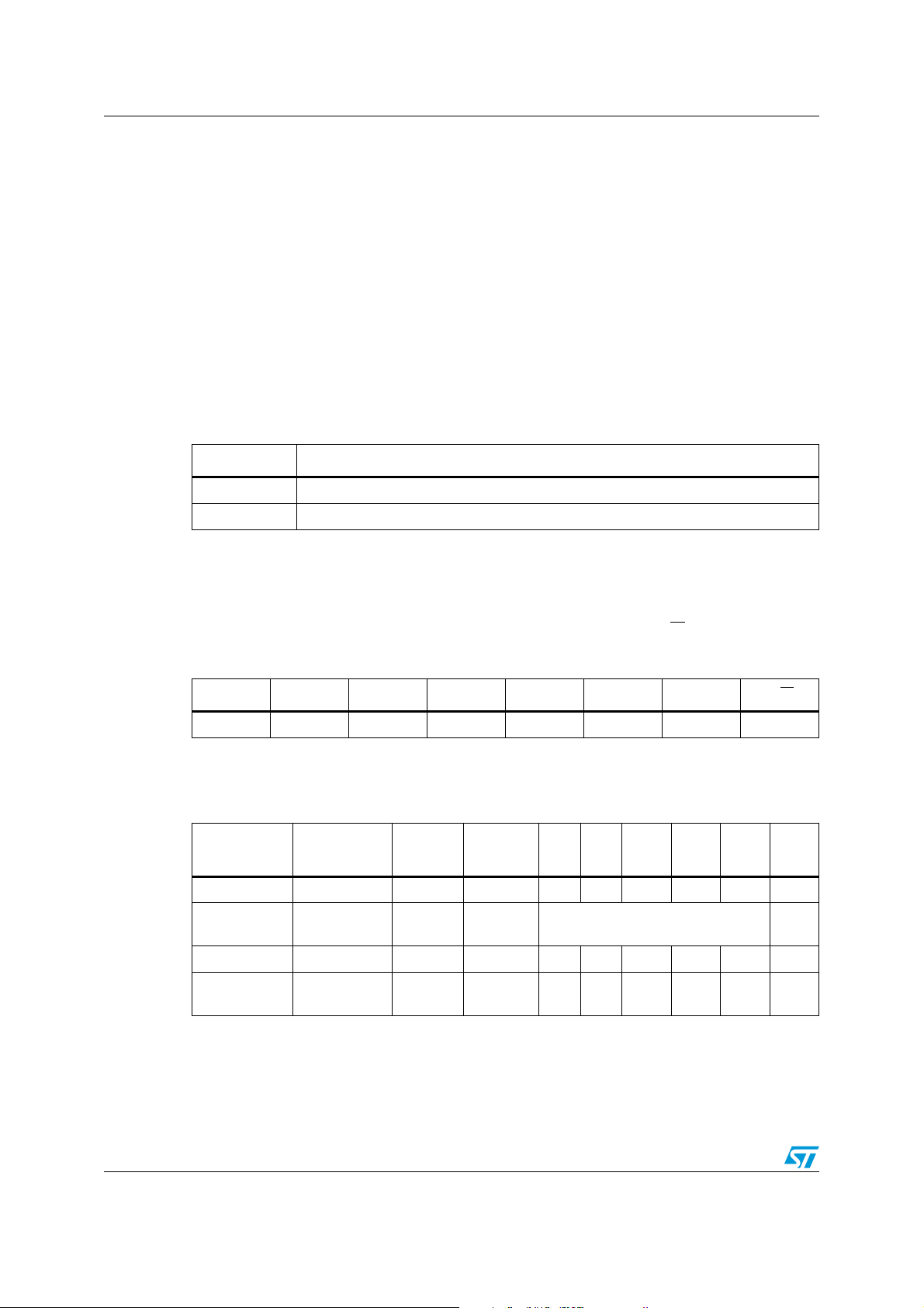
1 Absolute maximum ratings and operating conditions
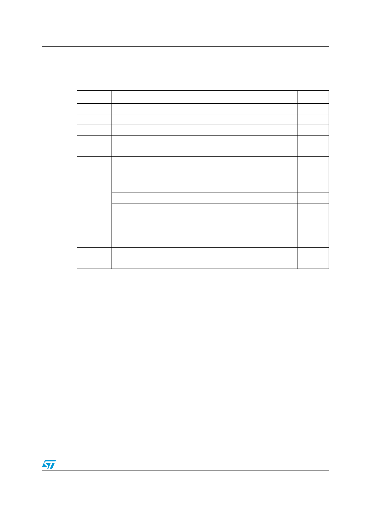
Table 1. Absolute maximum ratings
Symbol Parameter Value Unit
V
V
in+,Vin-
T
R
P
ESD
CC
stg
T
thja
Supply voltage
Input voltage referred to ground +/- 1.2 V
Storage temperature -65 to +150 °C
Maximum junction temperature
j
Thermal resistance junction to ambient
Power dissipation Internally limited
d
Human body model (HBM)
All pins
VOUTR, VOUTL vs. AGND
Machine model (MM), min. value
Charge device model (CDM)
All pins
VOUTR, VOUTL
IEC61000-4-2 level 4, contact
IEC61000-4-2 level 4, air discharge
(1)
during 1ms.
(5)
(7)
(2)
(6)
(7)
(3)
5.5 V
150 °C
200 °C/W
(4)
2
4
100 V
500
750
+/- 8
+/- 15
kV
V
kV
Latch-up Latch-up immunity 200 mA
Lead temperature (soldering, 10 sec) 260 °C
1. All voltage values are measured with respect to the ground pin.
2. Thermal shutdown is activated when maximum junction temperature is reached.
3. The device is protected from over-temperature by a thermal shutdown mechanism, active at 150° C.
4. Exceeding the power derating curves for long periods may provoke abnormal operation.
5. Human body model: a 100 pF capacitor is charged to the specified voltage, then discharged through a
1.5 kΩ resistor between two pins of the device. This is done for all couples of connected pin combinations
while the other pins are floating.
6. Machine model: a 200 pF capacitor is charged to the specified voltage, then discharged directly between
two pins of the device with no external series resistor (internal resistor < 5 Ω). This is done for all couples of
connected pin combinations while the other pins are floating.
7. The measurement is performed on an evaluation board, with ESD protection EMIF02-AV01F3.
Doc ID 022201 Rev 1 3/32

Absolute maximum ratings and operating conditions TS4621E
Table 2. Operating conditions
Symbol Parameter Value Unit
V
CC
Supply voltage 2.3 to 4.8 V
Buck DC output voltages
HPVDD
High rail voltage
Low rail voltage
1.9
1.2
SDA, SCL Input voltage range GND to V
T
R
R
C
oper
thja
L
L
Load resistor ≥ 16 Ω
Load capacitor
Serial resistor of 12 Ω minimum, R
≥ 16 Ω 0.8 to 100
L
Operating free air temperature range -40 to +85 °C
Flip-chip thermal resistance junction to ambient 90 °C/W
V
cc
V
nF
4/32 Doc ID 022201 Rev 1
TS4621E Typical application schematics
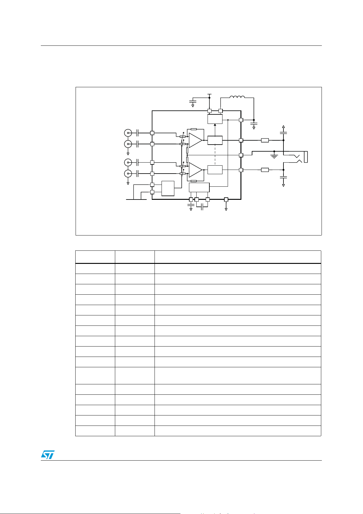
2 Typical application schematics
Figure 1. Typical application schematics for the TS4621E
Negative left in put
Positive left input
Negative rig ht input
Positive right input
I²C bus
Cin
2.2 uF
Cin
2.2 uF
Cin
2.2 uF
Cin
2.2 uF
InL+
InR-
SDA
SCL
InL-
InR+
I2C
Cs
2.2 uF
PVss
Css
2.2 uF
-
+
+
-
Negative
supply
AVdd
Vbat
detector
Positive
supply
Level
detector
Level
C12
2.2 uF
Sw
3.3 uH
HpVdd
VoutL
CMS
VoutR
AGndC1 C2
L1
Ct
10 uF
Rout
12 ohms min.
Rout
12 ohms min.
Cout
0.8 nF min.
3
J1
2
1
Cout
0.8 nF min.
Table 3. TS4621E pin description
Pin number Pin name Pin definition
A1 SW Switching node of the buck converter
A2 AVDD Analog supply voltage, connect to battery
A3 VOUTL Output signal for left audio channel
A4 INL- Negative input signal for left audio channel
B1 AGND Device ground
B2 C1 Flying capacitor terminal for internal negative supply generator
B3 HPVDD Buck converter output, power supply for amplifier
B4 INL+ Positive input signal for left audio channel
C1 C2 Flying capacitor terminal for internal negative supply generator
C2 PVSS Negative supply generator output
C3 CMS
Common mode sense, to be connected as close as possible to the
ground of headphone/line out plug
C4 INR+ Positive input signal for right audio channel
D1 SDA I²C data signal, up to V
D2 SCL I²C clock signal, up to V
tolerant input
CC
tolerant input
CC
D3 VOUTR Output signal for right audio channel
D4 INR- Negative input signal for right audio channel
AM06119
Doc ID 022201 Rev 1 5/32
Typical application schematics TS4621E
Table 4. TS4621E component description
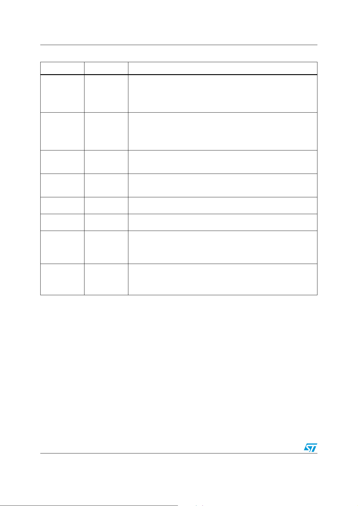
Component Value Description
Cs 2.2 µF
C12 2.2 µF
C
SS
C
in
C
out
R
out
2.2 µF
Cin
------------------------=
2π ZinFc
0.8 to 100 nF
12 Ω min.
L1 3.3 µH
Decoupling capacitors for V
. A 2.2 µF capacitor is sufficient for proper
CC
decoupling of the TS4621E. An X5R dielectric and 10 V rating voltage is
recommended to minimize ΔC/ΔV when V
CC
=4.8V.
Must be placed as close as possible to the TS4621E to minimize parasitic
inductance and resistance.
Capacitor for internal negative power supply operation. An X5R dielectric and
6.3 V rating voltage is recommended to minimize ΔC/ΔV when
HPVDD = 1.9 V.
Must be placed as close as possible to the TS4621E to minimize parasitic
inductance and resistance.
Filtering capacitor for internal negative power supply. An X5R dielectric and
6.3 V rating voltage is recommended to minimize ΔC/ΔV when
HPVDD = 1.9 V.
1
Input coupling capacitor that forms with Zin/2 a first-order high-pass filter with
a -3 dB cutoff frequency FC. For example, at maximum gain G = 4 dB,
Zin = 12.5 kΩ, C
= 2.2 µF, therefore FC = 6 Hz.
in
Output capacitor of 0.8 nF minimum to 100 nF maximum. This capacitor is
mandatory for operation of the TS4621E.
Output resistor in-series with the TS4621E output. This 12 Ω minimum resistor
is mandatory for operation of the TS4621E.
Inductor for the buck convertor.
References of inductors:
FDK: MIPSZ2012D3R3 (DC resistance = 0.19 Ω, rated current = 0.8 A)
Murata: LQM2MPN3R3G0 (DC resistance = 0.12 Ω, rated current = 1.2 A)
Tank capacitor for internal buck convertor. An X5R dielectric and 6.3 V rating
C
t
10 µF
voltage is recommended to minimize ΔC/ΔV when HPVDD = 1.9 V.
ESR of the C
capacitor must be as low as possible to obtain the best buck
t
efficiency.
6/32 Doc ID 022201 Rev 1
TS4621E Electrical characteristics
3 Electrical characteristics
Table 5. Electrical characteristics of the I²C interface
for V
= +3.6 V, AGND = 0 V, T
CC
= 25°C (unless otherwise specified)
amb
Symbol Parameter Min. Typ. Max. Unit
V
V
V
Table 6. Electrical characteristics of the amplifier
Low level input voltage on SDA, SCL pins 0.6 V
IL
High level input voltage on SDA, SCL pins 1.2 V
IH
Low level output voltage, SDA pin, I
OL
Input current on SDA, SCL 10 µA
I
in
for V
= +3.6 V, AGND = 0 V, RL= 32 Ω + 15 Ω, T
CC
= 3mA 0.4 V
sink
V
SDA SCL,
------------------------------ -- -
600k Ω
= 25° C
amb
(unless otherwise specified)
Symbol Parameter Min. Typ. Max. Unit
I
I
STBY
V
V
V
Quiescent supply current, no input signal, both channels
CC
enabled
Supply current, with input modulation, both channels enabled,
HPVDD = 1.2 V, output power per channel, F=1kHz
Pout = 100 µW at 3 dB crest factor
I
s
Pout = 500 µW at 3 dB crest factor
Pout = 1mW at 3dB crest factor
Pout = 100 µW at 10 dB crest factor
Pout = 500 µW at 10 dB crest factor
Pout = 1 mW at 10 dB crest factor
Standby current, no input signal, I²C CR1 = 01h
= 0 V, V
V
SDA
Input differential voltage range
in
SCL
= 0 V
(1)
Output offset voltage
oo
No input signal
Maximum output voltage, in-phase signals
= 16 Ω, THD+N = 1% max, f = 1 kHz
R
L
= 47 Ω, THD+N = 1% max, f = 1 kHz
out
R
L
RL = 10 kΩ, Rs = 15 Ω, CL = 1 nF, THD+N = 1% max,
f = 1 kHz
1.2 1.5 mA
2.3
3.7
4.7
3.5
5
6.5
2.1
3.1
3.9
0.6 5 µA
1V
-500 +500 µV
0.6
1.0
1.0
0.8
1.1
1.3
mA
V
rms
rms
THD+N
PSRR
Total harmonic distortion + noise, G = 0 dB
= 700 mVrms, F = 1 kHz
V
out
= 700 mVrms, 20 Hz < F < 20 kHz
V
out
(1)
, V
Power supply rejection ratio
= 200 mVpp, grounded
ripple
inputs
F = 217 Hz, G = 0 dB, R
F = 10 kHz, G = 0 dB, R
≥16 Ω
L
≥16 Ω
L
Doc ID 022201 Rev 1 7/32
0.006
0.05
90 100
70
0.02 %
dB
Electrical characteristics TS4621E
Table 6. Electrical characteristics of the amplifier
for V
= +3.6 V, AGND = 0 V, RL= 32 Ω + 15 Ω, T
CC
amb
= 25° C
(unless otherwise specified) (continued)
Symbol Parameter Min. Typ. Max. Unit
Common mode rejection ratio
CMRR
F = 1 kHz, G = 0 dB, V
F = 20 Hz to 20 kHz, G = 0 dB, Vic = 200 mV
= 200 mV
ic
pp
65
pp
45
Channel separation
Crosstalk
SNR
ONoise
= 32 Ω + 15 Ω , G = 0 dB, F = 1 kHz, Po = 10 mW
R
L
= 10 kΩ, G = 0 dB, F = 1 kHz, V
R
L
Signal-to-noise ratio, A-weighted, V
F = 1 kHz
(1)
out
out
= 1 V
=1 Vrms
G = +4 dB
G = +0 dB
Output noise voltage, A-weighted
(1)
G = +4 dB
, THD+N < 1%,
rms
60
80
99
100
100
110
9119µVrms
G = +0 dB
G Gain range with gain (dB) = 20 x log[(V
Mute InL/R+ - InL/R- = 1 V
rms
L/R)/(InL/R+ - InL/R-)] -60 +4 dB
out
- Gain step size error -0.5 +0.5
-80 dB
dB
dB
dB
step-
size
- Gain error (G = +4 dB) -0.45 +0.42 dB
Z
Differential input impedance 25 34 kΩ
in
Input impedance during wake-up phase (referred to ground) 2 kΩ
Output impedance when CR1 = 00h (negative supply is ON and
amplifier output stages are OFF)
Z
out
F < 40 kHz
F = 6 MHz
F = 36 MHz
t
t
stby
t
t
1. Guaranteed by design and parameter correlation.
2. Refer to the application information in Section 4.3 on page 27.
Wake-up time
wu
Standby time 100 µs
Attack time. Setup time between low rail buck voltage and high
atk
rail buck voltage
Decay time 50 ms
dcy
(2)
(1)
10
500
75
12 16 ms
100 µs
kΩ
Ω
Ω
8/32 Doc ID 022201 Rev 1
TS4621E Electrical characteristics
Table 7. Timing characteristics of the I²C interface for I²C interface signals over
recommended operating conditions (unless otherwise specified)
Symbol Parameter Min. Typ. Max. Unit
f
SCL
t
d(H)
t
d(L)
t
t
t
t
t
Frequency, SCL 400 kHz
Pulse duration, SCL high 0.6 µs
Pulse duration, SCL low 1.3 µs
Setup time, SDA to SCL 100 ns
st1
Hold time, SCL to SDA 0 ns
h1
Bus free time between stop and start condition 1.3 µs
t
f
Setup time, SCL to start condition 0.6 µs
st2
Hold time, start condition to SCL 0.6 µs
h2
Setup time, SCL to stop condition 0.6 µs
st3
Figure 2. SCL and SDA timing diagram
t
d(H)
t
SCL
SDA
d(L)
t
st1
t
h1
Figure 3. Start and stop condition timing diagram
SCL
t
t
st2
h2
SDA
Start condition Stop condition
AM06113
t
f
t
st3
AM06114
Doc ID 022201 Rev 1 9/32
Electrical characteristics TS4621E
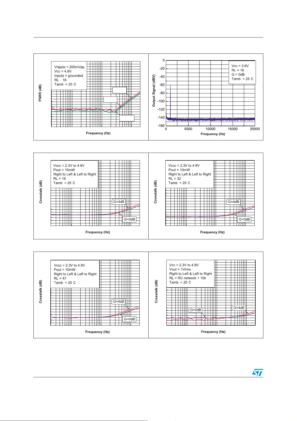
No load; No input Signal
SDA=SCL = 0V
Ta = 25°C
2.3 2.7 3.1 3.5 3.9 4.3 4.7
0
20
40
60
80
THD+N=10% (180°)
THD+N=10% (0°)
THD+N=1% (0°)
RL = 32Ω, F = 1kHz
BW < 30kHz, Tamb = 25°C
THD+N=1% (180°)
Output power (mW)
Power Supply Voltage Vcc (V)
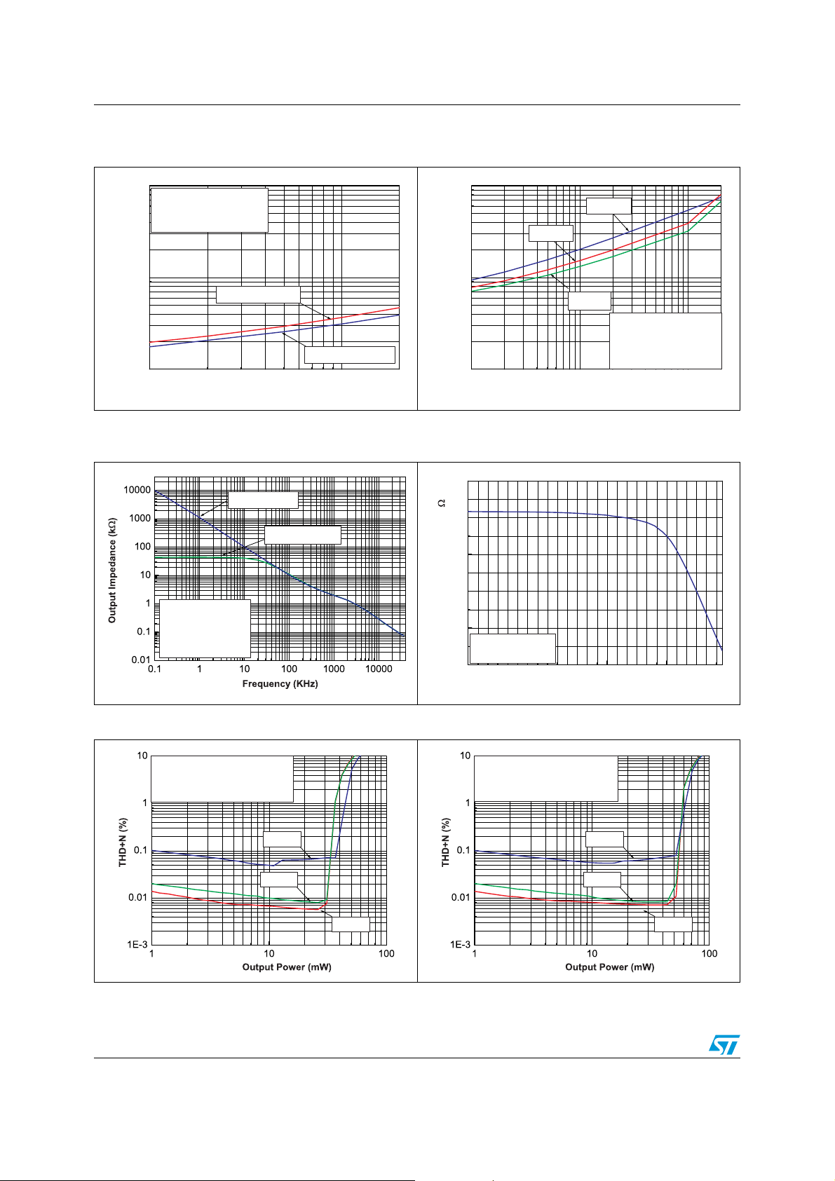
Figure 4. Current consumption vs. power
(mA)
CC
Quiscent Supply Current I
supply voltage
1.6
1.4
1.2
1.0
0.8
0.6
0.4
0.2
0.0
2.4 2.6 2.8 3.0 3.2 3.4 3.6 3.8 4.0 4.2 4.4 4.6 4.8
Power Supply Voltage Vcc (V)
No load; No input Signal
Both channels enabled
Ta = 25°C
Figure 5. Standby current consumption vs.
power supply voltage
Figure 6. Maximum output power vs. load Figure 7. Maximum output power vs. load
80
70
60
50
40
30
20
Output power (mW)
10
0
10 100 1k
VCC=4.8V
VCC=3.6V
VCC=2.3V
RL Load resistance ( )
Inputs = 0°, F = 1kHz
THD+N = 1%
Tamb = 25°C
80
70
60
50
40
30
20
Output power (mW)
10
0
10 100 1k
VCC=4.8V
VCC=3.6V
VCC=2.3V
RL Load resistance ( )
Inputs = 180°, F = 1kHz
THD+N = 1%
Tamb = 25°C
Figure 8. Maximum output power vs. power
supply voltage
RL = 16Ω, F = 1kHz
120
BW < 30kHz, Tamb = 25°C
100
80
60
40
Output power (mW)
20
0
2.3 2.7 3.1 3.5 3.9 4.3 4.7
10/32 Doc ID 022201 Rev 1
THD+N=10% (0°)
THD+N=1% (180°)
Power Supply Voltage Vcc (V)
Figure 9. Maximum output power vs. power
supply voltage
THD+N=10% (180°)
THD+N=1% (0°)

TS4621E Electrical characteristics
2.3 2.7 3.1 3.5 3.9 4.3 4.7
700
800
900
1000
1100
1200
1300
1400
1500
1600
10 K
Ω
600
Ω
60
Ω
47
Ω
16
Ω
F = 1kHz
BW < 30kHz, Tamb = 25°C
Inputs = 0°, THD+N = 1%
32
Ω
Output Voltage (mVrms)
Power Supply Voltage Vcc (V)
0.1 1 10
1
10
100
Vcc=4.8V
Vcc=3.6V
Vcc=2.3V
Both channels enabled
RL = 16Ω, F = 1KHz
Ta = 25°C
Crest Factor = 3dB
Supply Current I
S
(mA)
Total Output Power (mW)
0.1 1 10
1
10
100
Vcc=4.8V
Vcc=3.6V
Vcc=2.3V
Both channels enabled
RL = 47Ω, F = 1 KHz
Ta = 25°C
Crest Factor = 3dB
Supply Current I
S
(mA)
Total Output Power (mW)
Figure 10. Maximum output power vs. power
supply voltage
RL = 47Ω, F = 1kHz
BW < 30kHz, Tamb = 25°C
60
THD+N=10% (0°)
THD+N=10% (180°)
40
20
Output power (mW)
THD+N=1% (180°)
0
2.3 2.7 3.1 3.5 3.9 4.3 4.7
Power Supply Voltage Vcc (V)
THD+N=1% (0°)
Figure 12. Maximum output voltage vs. power
supply voltage
1600
1500
1400
1300
1200
1100
1000
Output Voltage (mVrms)
F = 1kHz
BW < 30kHz, Tamb = 25°C
Inputs = 180°, THD+N=1%
47
16
Ω
Ω
32
Ω
900
800
700
2.3 2.7 3.1 3.5 3.9 4.3 4.7
Power Supply Voltage Vcc (V)
60
600
Ω
Ω
10 K
Ω
Figure 11. Maximum output voltage vs. power
supply voltage
Figure 13. Current consumption vs. total
output power
Figure 14. Current consumption vs. total
output power
100
Both channels enabled
RL = 32Ω, F = 1KHz
Ta = 25°C
Crest Factor = 3dB
(mA)
S
10
Supply Current I
1
0.1 1 10
Vcc=3.6V
Total Output Power (mW)
Figure 15. Current consumption vs. total
output power
Vcc=2.3V
Vcc=4.8V
Doc ID 022201 Rev 1 11/32
Electrical characteristics TS4621E
-60 -55 -50 -45 -40 -35 -30 -25 -20 -15 -10 -5 0
30
40
50
60
70
80
Vcc=2.3V to 4.8V
Ta = 25°C
Differential Input Impedance (K )
Gain (dB)
Figure 16. Current consumption vs. total
100
(mA)
S
Supply Current I
output power
Both channels enabled
RL = 47Ω, F = 1KHz
Ta = 25°C, Vcc = 3.6V
10
Crest Factor=3dB
Crest Factor=10dB
1
0.1 1
Total Output Power (mW)
Figure 17. Power dissipation vs. total output
power
100
R = 16
Ω
R = 32
Ω
10
R = 47
Ω
Power Dissipation (mW)
1
0.1 1 10
Total Output Power (mW)
Both channels enabled
F = 1KHz,
Ta = 25°C
Crest Factor = 3dB
Figure 18. Output impedance vs. frequency Figure 19. Differential input impedance vs.
gain
Input Floating
Input grounded
Vcc=2.3V to 4.8V
HIz; Right & Left
Osc level=0.5V
Ta = 25°C
RMS
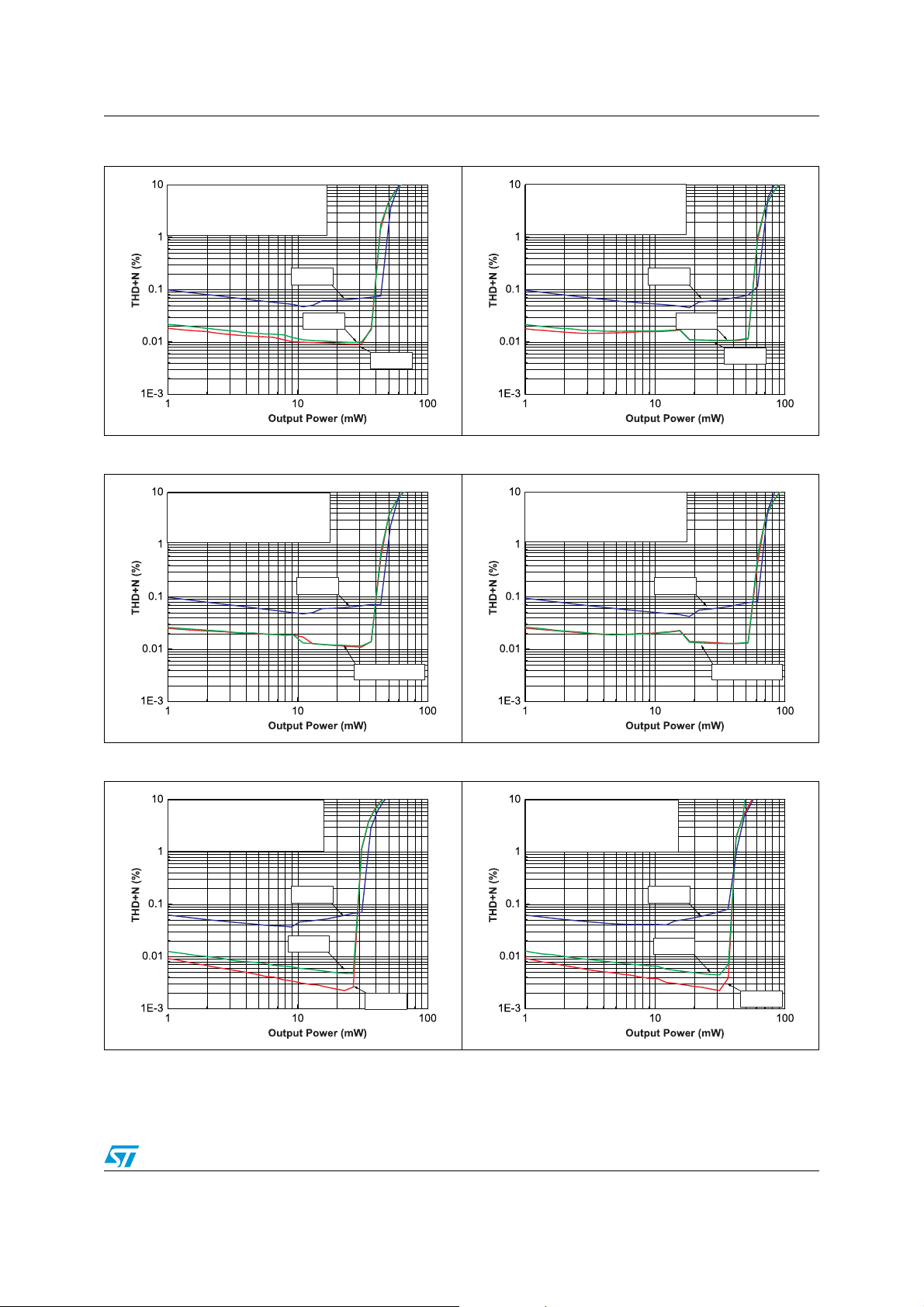
Figure 20. THD+N vs. output power Figure 21. THD+N vs. output power
Vcc = 2.5V, RL = 16
G = 4dB, Inputs = 0
Ω
°
BW < 30kHz, Tamb = 25°C
F=8kHz
F=1kHz
F=80Hz
Vcc = 2.5V, RL = 16
G = 4dB, Inputs = 180
BW < 30kHz, Tamb = 25°C
Ω
°
F=8kHz
F=1kHz
F=80Hz
12/32 Doc ID 022201 Rev 1
TS4621E Electrical characteristics
Figure 22. THD+N vs. output power Figure 23. THD+N vs. output power
Vcc = 3.6V, RL = 16
G = 4dB, Inputs = 0
Ω
°
BW < 30kHz, Tamb = 25°C
F=8kHz
Vcc = 3.6V, RL = 16
G = 4dB, Inputs = 180
BW < 30kHz, Tamb = 25°C
F=1kHz
F=80Hz
Ω
°
F=8kHz
F=1kHz
Figure 24. THD+N vs. output power Figure 25. THD+N vs. output power
Vcc = 4.8V, RL = 16
G = 4dB, Inputs = 0
Ω
°
BW < 30kHz, Tamb = 25°C
F=8kHz
Vcc = 4.8V, RL = 16
G = 4dB, Inputs = 180
BW < 30kHz, Tamb = 25°C
Ω
°
F=8kHz
F=80Hz
F=80Hz, 1kHz
F=80Hz, 1kHz
Figure 26. THD+N vs. output power Figure 27. THD+N vs. output power
Vcc = 2.5V, RL = 32
G = 4dB, Inputs = 0
BW < 30kHz, Tamb = 25°C
Ω
°
F=8kHz
F=1kHz
F=80Hz
Vcc = 2.5V, RL = 32
G = 4dB, Inputs = 180
Ω
°
BW < 30kHz, Tamb = 25°C
F=8kHz
F=1kHz
F=80Hz
Doc ID 022201 Rev 1 13/32

Electrical characteristics TS4621E
Figure 28. THD+N vs. output power Figure 29. THD+N vs. output power
Vcc = 3.6V, RL = 32
G = 4dB, Inputs = 0
Ω
°
BW < 30kHz, Tamb = 25°C
F=8kHz
Vcc = 3.6V, RL = 32
G = 4dB, Inputs = 180
BW < 30kHz, Tamb = 25°C
F=1kHz
F=80Hz
Ω
°
F=8kHz
F=1kHz
F=80Hz
Figure 30. THD+N vs. output power Figure 31. THD+N vs. output power
Vcc = 4.8V, RL = 32
G = 4dB, Inputs = 0
BW < 30kHz, Tamb = 25°C
Ω
°
F=8kHz
Vcc = 4.8V, RL = 32
G = 4dB, Inputs = 180
Ω
°
BW < 30kHz, Tamb = 25°C
F=8kHz
F=1kHz
F=80Hz
F=1kHz
Figure 32. THD+N vs. output power Figure 33. THD+N vs. output power
Vcc = 2.5V, RL = 47
G = 4dB, Inputs = 0
Ω
°
BW < 30kHz, Tamb = 25°C
F=8kHz
F=1kHz
Vcc = 2.5V, RL = 47
G = 4dB, Inputs = 180
BW < 30kHz, Tamb = 25°C
F=80Hz
Ω
°
F=8kHz
F=1kHz
F=80Hz
F=80Hz
14/32 Doc ID 022201 Rev 1

TS4621E Electrical characteristics
Po=1mW
Po=15mW
RL = 16Ω
Vcc = 2.5V
G = 0dB
Inputs = 180°
Bw < 20kHz
Tamb = 25°C
20k20
Figure 34. THD+N vs. output power Figure 35. THD+N vs. output power
Vcc = 3.6V, RL = 47
G = 4dB, Inputs = 0
Ω
°
BW < 30kHz, Tamb = 25°C
F=8kHz
F=1kHz
Vcc = 3.6V, RL = 47
G = 4dB, Inputs = 180
BW < 30kHz, Tamb = 25°C
F=80Hz
Ω
°
F=8kHz
F=1kHz
Figure 36. THD+N vs. output power Figure 37. THD+N vs. output power
Vcc = 4.8V, RL = 47
G = 4dB, Inputs = 0
Ω
°
BW < 30kHz, Tamb = 25°C
F=8kHz
Vcc = 4.8V, RL = 47
G = 4dB, Inputs = 180
BW < 30kHz, Tamb = 25°C
Ω
°
F=8kHz
F=80Hz
Figure 38. THD+N vs. frequency Figure 39. THD+N vs. frequency
RL = 16Ω
Vcc = 2.5V
G = 0dB
Inputs = 0°
Bw < 20kHz
Tamb = 25°C
F=1kHz
Po=1mW
F=80Hz
Po=15mW
F=1kHz
F=80Hz
20k20
Doc ID 022201 Rev 1 15/32
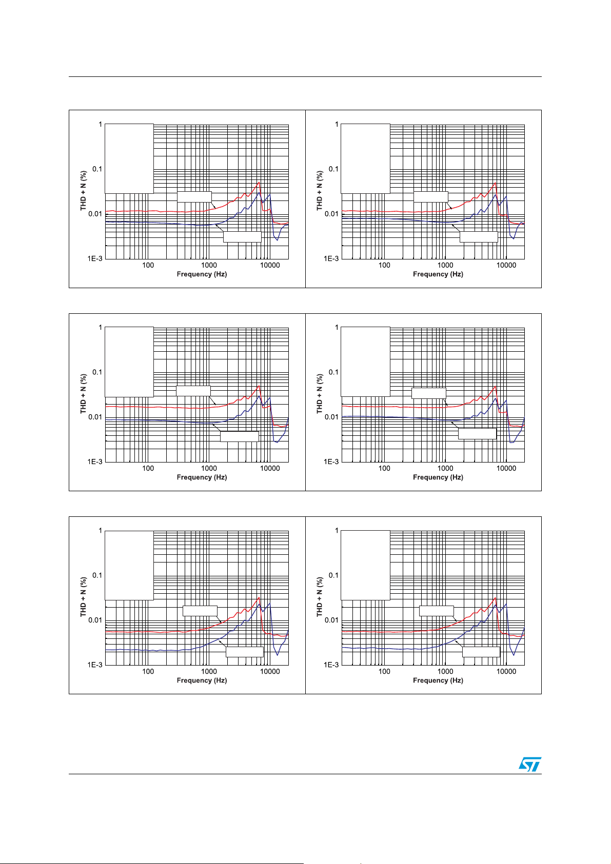
Electrical characteristics TS4621E
Po=1mW
Po=15mW
RL = 16Ω
Vcc = 3.6V
G = 0dB
Inputs = 180°
Bw < 20kHz
Tamb = 25°C
20k20
Po=1mW
Po=15mW
RL = 16Ω
Vcc = 4.8V
G = 0dB
Inputs = 180°
Bw < 20kHz
Tamb = 25°C
20k20
Po=1mW
Po=10mW
RL = 32Ω
Vcc = 2.5V
G = 0dB
Inputs = 180°
Bw < 20kHz
Tamb = 25°C
20k20
Figure 40. THD+N vs. frequency Figure 41. THD+N vs. frequency
RL = 16Ω
Vcc = 3.6V
G = 0dB
Inputs = 0°
Bw < 20kHz
Tamb = 25°C
Po=1mW
Po=15mW
20k20
Figure 42. THD+N vs. frequency Figure 43. THD+N vs. frequency
RL = 16Ω
Vcc = 4.8V
G = 0dB
Inputs = 0°
Bw < 20kHz
Tamb = 25°C
Po=1mW
Figure 44. THD+N vs. frequency Figure 45. THD+N vs. frequency
16/32 Doc ID 022201 Rev 1
RL = 32Ω
Vcc = 2.5V
G = 0dB
Inputs = 0°
Bw < 20kHz
Tamb = 25°C
Po=15mW
20k20
Po=1mW
Po=10mW
20k20
TS4621E Electrical characteristics
Po=1mW
Po=10mW
RL = 32Ω
Vcc = 3.6V
G = 0dB
Inputs = 180°
Bw < 20kHz
Tamb = 25°C
20k20
Po=1mW
Po=10mW
RL = 32Ω
Vcc = 4.8V
G = 0dB
Inputs = 180°
Bw < 20kHz
Tamb = 25°C
20k20
Po=1mW
Po=10mW
RL = 47Ω
Vcc = 2.5V
G = 0dB
Inputs = 180°
Bw < 20kHz
Tamb = 25°C
20k20
Figure 46. THD+N vs. frequency Figure 47. THD+N vs. frequency
RL = 32Ω
Vcc = 3.6V
G = 0dB
Inputs = 0°
Bw < 20kHz
Tamb = 25°C
Po=1mW
Po=10mW
20k20
Figure 48. THD+N vs. frequency Figure 49. THD+N vs. frequency
RL = 32Ω
Vcc = 4.8V
G = 0dB
Inputs = 0°
Bw < 20kHz
Tamb = 25°C
Po=1mW
Po=10mW
20k20
Figure 50. THD+N vs. frequency Figure 51. THD+N vs. frequency
RL = 47Ω
Vcc = 2.5V
G = 0dB
Inputs = 0°
Bw < 20kHz
Tamb = 25°C
Po=1mW
Po=10mW
20k20
Doc ID 022201 Rev 1 17/32

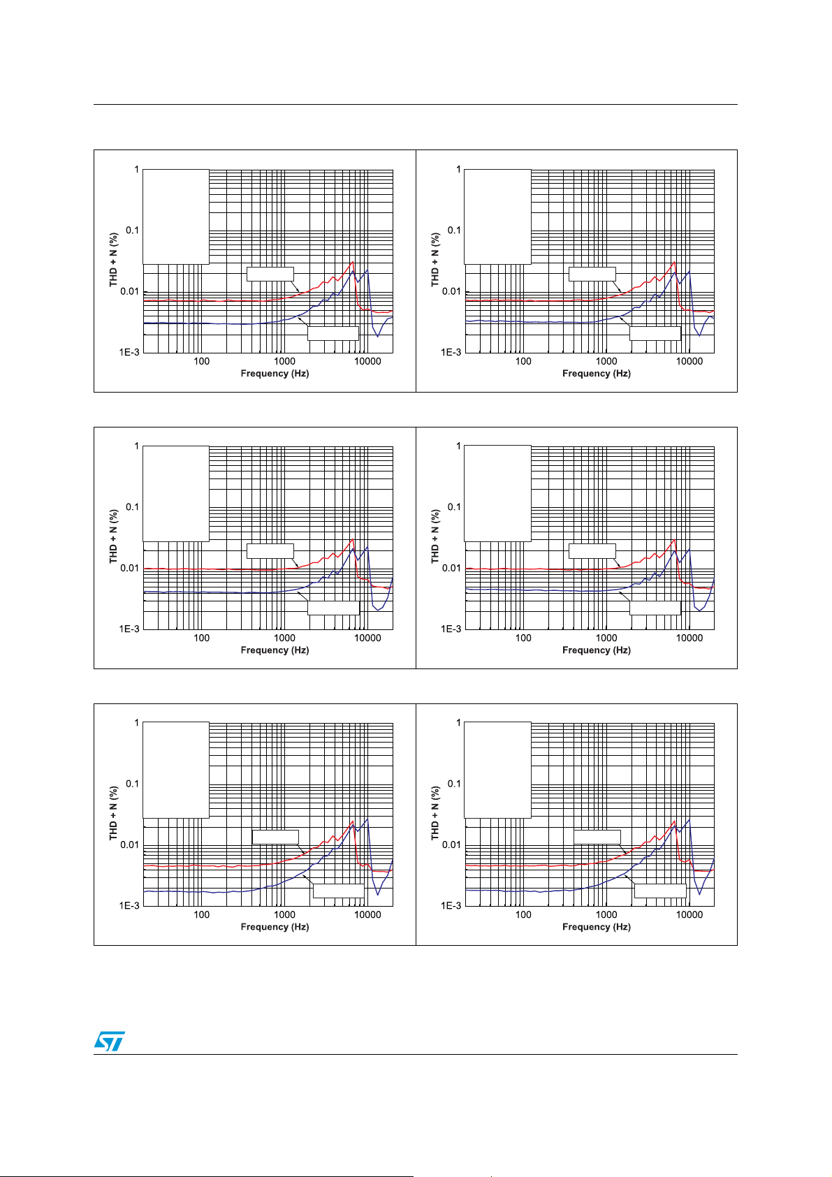
Electrical characteristics TS4621E
Po=1mW
Po=10mW
RL = 47Ω
Vcc = 3.6V
G = 0dB
Inputs = 180°
Bw < 20kHz
Tamb = 25°C
20k20
Po=1mW
Po=10mW
RL = 47Ω
Vcc = 4.8V
G = 0dB
Inputs = 180°
Bw < 20kHz
Tamb = 25°C
20k20
Vo=1Vrms
Vo=100mVrms
RL = RC network + 600Ω
Vcc = 2.3V to 4.8V
G = 0dB, Inputs = 0° & 180°
Bw < 20kHz, Tamb = 25°C
20k20
Figure 52. THD+N vs. frequency Figure 53. THD+N vs. frequency
RL = 47Ω
Vcc = 3.6V
G = 0dB
Inputs = 0°
Bw < 20kHz
Tamb = 25°C
Po=1mW
Po=10mW
20k20
Figure 54. THD+N vs. frequency Figure 55. THD+N vs. frequency
RL = 47Ω
Vcc = 4.8V
G = 0dB
Inputs = 0°
Bw < 20kHz
Tamb = 25°C
Po=1mW
Po=10mW
20k20
Figure 56. THD+N vs. frequency Figure 57. THD+N vs. frequency
RL = RC network + 10kΩ
Vcc = 2.3V to 4.8V
G = 0dB, Inputs = 0° & 180°
Bw < 20kHz, Tamb = 25°C
Vo=100mVrms
Vo=1Vrms
20k20
18/32 Doc ID 022201 Rev 1

TS4621E Electrical characteristics
F=80Hz
F=1kHz
F=8kHz
RL = RC network + 600
Ω
Vcc = 2.3V to 4.8V, G = 4dB
Inputs = 0° & 180
°
BW < 30kHz, Tamb = 25°C
100 1000 10000
-80
-70
-60
-50
-40
-30
-20
-10
0
20k
20
Δ
≥ Ω
°
100 1000 10000
-130
-120
-110
-100
-90
-80
-70
-60
-50
-40
-30
-20
-10
0
G=-6dB
G=0dB
G=4dB
20k
20
≥ Ω
°
Figure 58. THD+N vs. output voltage Figure 59. THD+N vs. output voltage
RL = RC network + 10k
Vcc = 2.3V to 4.8V, G = 4dB
Inputs = 0° & 180
BW < 30kHz, Tamb = 25°C
Figure 60. THD+N vs. input voltage, HiZ left
Ω
°
F=8kHz
F=1kHz
F=80Hz
Figure 61. CMRR vs. frequency
and right
HiZ Left & Right
Vcc = 2.3V to 4.8V
Zout generator = 1k
BW < 30kHz, Tamb = 25°C
Ω
Line In F=8kHz
Line In F=1kHz
Line In F=80Hz
Figure 62. PSRR vs. frequency Figure 63. PSRR vs. frequency
Reference F=80Hz, 1kHz, 8kHz
0
-10
-20
-30
≥ Ω
-40
-50
-60
-70
°
G=4dB
G=0dB
-80
-90
-100
-110
G=-6dB
-120
-130
20
100 1000 10000
20k
Doc ID 022201 Rev 1 19/32
Electrical characteristics TS4621E
Ω
°
100 1000 10000
-120
-110
-100
-90
-80
-70
-60
-50
-40
-30
-20
-10
0
20k
20
Ω
°
100 1000 10000
-130
-120
-110
-100
-90
-80
-70
-60
-50
-40
-30
-20
-10
0
20k
20
Ω
°
Figure 64. PSRR vs. frequency Figure 65. Output signal spectrum
0
-10
-20
-30
≥ Ω
-40
-50
-60
-70
-80
°
G=4dB
G=0dB
-90
-100
-110
-120
-130
20
100 1000 10000
G=-6dB
20k
Figure 66. Crosstalk vs. frequency Figure 67. Crosstalk vs. frequency
0
-10
-20
-30
-40
-50
-60
-70
-80
-90
-100
-110
-120
20
Ω
°
100 1000 10000
20k
Figure 68. Crosstalk vs. frequency Figure 69. Crosstalk vs. frequency
0
-10
-20
-30
-40
-50
-60
-70
-80
-90
-100
-110
-120
20
20/32 Doc ID 022201 Rev 1
Ω
°
100 1000 10000
20k
TS4621E Electrical characteristics
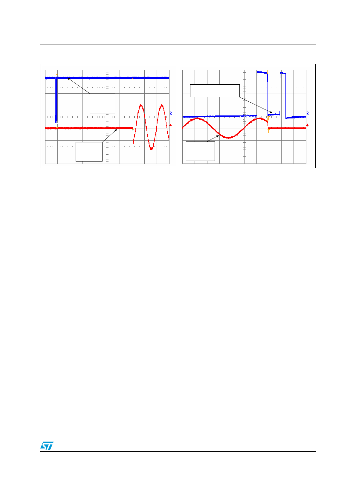
Figure 70. Wake-up time Figure 71. Shutdown time
I²C ACK after
SDA
2 ms/div
1V/div
VOUT
2ms/div
20mv/div
Shutdown command
VOUT
10µs/div
100mv/div
Doc ID 022201 Rev 1 21/32
Application information TS4621E
4 Application information
4.1 I2C bus interface
In compliance with the I²C protocol, the TS4621E uses a serial bus to control the chip’s
functions with the clock (SCL) and data (SDA) wires. These two lines are bi-directional
(open collector) and require an external pull-up resistor (typically 10 kΩ). The maximum
clock frequency in fast mode specified by the I²C standard is 400 kHz, which the TS4621E
supports. In this application, the TS4621E is always the slave device and the controlling
microcontroller MCU is the master device.
The slave address of the TS4621E is 1100 000x (C0h).
Ta bl e 8 summarizes the pin descriptions for the I²C bus interface.
Table 8. I²C bus interface pin descriptions
Pin Functional description
SDA Serial data pin
SCL Clock input pin
4.1.1 I²C bus operation
The host MCU can write to the TS4621E control register to control the TS4621E, and read
from the control register to obtain a configuration from the TS4621E. The TS4621E is
addressed by the byte consisting of the 7-bit slave address and the R/W
Table 9. First byte after the START message for addressing the device
A6 A5 A4 A3 A2 A1 A0 R/W
1100000X
There are four control registers (Tab le 1 0) named CR1 to CR4. In read mode, all the control
registers can be accessed. In write mode, only CR1, CR2 and CR3 can be addressed.
Table 10. Summary of control registers
Description
CR1 1 HP_EN_L HP_EN_R 0 0 SC_L SC_R T_SH SWS
CR2
volume control
CR3 3 0 0 0 0 0 0 HiZ_L HiZ_R
CR4
identification
Register
address
bit.
D7 D6 D5 D4 D3 D2 D1 D0
2
4
Mute_L Mute_R Volume control 0
0 1 000000
22/32 Doc ID 022201 Rev 1

TS4621E Application information
Writing to the control registers
To write data to the TS4621E, after the "start" message the MCU must:
● send the I²C 7-bit slave address and a low level for the R/W bit.
● send the register address to write to.
● send the data bytes (control register settings).
All bytes are sent MSB first. The transfer of written data ends with a "stop" message. When
transmitting several data bytes, the data can be written without having to repeat the "start"
message or send the byte with the slave address. If several bytes are transmitted, they will
be written repeatedly to CR1, CR2 and CR3.
Figure 72. I²C write operations
DATA BYTES
SLAVE DEVICE ADDRESS
SDA
REGISTER ADDRESS
CR X
CRX+1
S
1100
Start
condition
ACK
00 A7
0
0
R/W
Acknowledge
from slave
A6
A1
A0
ACK
D7
D6
D1 D0
ACK
D7 D6
D1 D0
Acknowledge
from slave
ACK P
Stop
condition
AM06115
Reading from the control registers
To read data from the TS4621E, after the "start" message the MCU must:
● send the I²C 7-bit slave address and a low level for the R/W bit.
● send the register address to write to.
● send the I²C 7-bit slave address and a high level for the R/W bit.
● receive the data (control register value).
All bytes are read MSB first. The transfer of read data ends with a "stop" message. When
transmitting several data bytes, the data can be read without having to repeat the "start"
message or send the byte with the slave address. If several bytes are transmitted, they will
be read repeatedly from CR1, CR2, CR3 and CR4.
Doc ID 022201 Rev 1 23/32

Application information TS4621E
Figure 73. I²C read operations
DATA BYTES
CRX CRX+1
SDA
DEVICE ADDRESS
REGISTER ADDRESS
DEVICE ADDRESS
110
S
Start condition
00
000
ACK
R/W
Acknowledge
fom slave
A7 A0
ACK
S
Repeat
start condition
110
00100
ACK ACK
R/W
D7
D0
D7
AA
D0
condition
Not
Acknowledge
AM06116
4.1.2 Control register CR2 - address 2
Table 11. Volume control register CR2 - address 2
D5 D4 D3 D2 D1
00000 -60 dB 10000 -11 dB
00001 -54 dB 10001 -10 dB
00010-50.5 dB 10010 -9 dB
00011 -47 dB 10011 -8 dB
00100 -43 dB 10100 -7 dB
Volume control range: -60 dB to +4 dB
Gain
(in dB)
D5 D4 D3 D2 D1
Gain
(in dB)
P
Stop
00101 -39 dB 10101 -6 dB
00110 -35 dB 10110 -5 dB
00111 -31 dB 10111 -4 dB
01000 -27 dB 11000 -3 dB
01001 -25 dB 11001 -2 dB
01010 -23 dB 11010 -1 dB
01011 -21 dB 11011 0 dB
01100 -19 dB 11100 +1 dB
01101 -17 dB 11101 +2 dB
01110 -15 dB 11110 +3 dB
01111 -13 dB 11111 +4 dB
Mute function: bits MUTE_L and MUTE_R
In the volume register, MUTE_L and MUTE_R are dedicated to enabling the mute function,
independently of the channel. When MUTE_L and MUTE_R are set to V
function is enabled on the corresponding channel and the gain is set to -80 dB. When
MUTE_L and MUTE_R are set to V
24/32 Doc ID 022201 Rev 1
, the I²C gain level is applied to the channel.
IL
, the mute
IH
TS4621E Application information
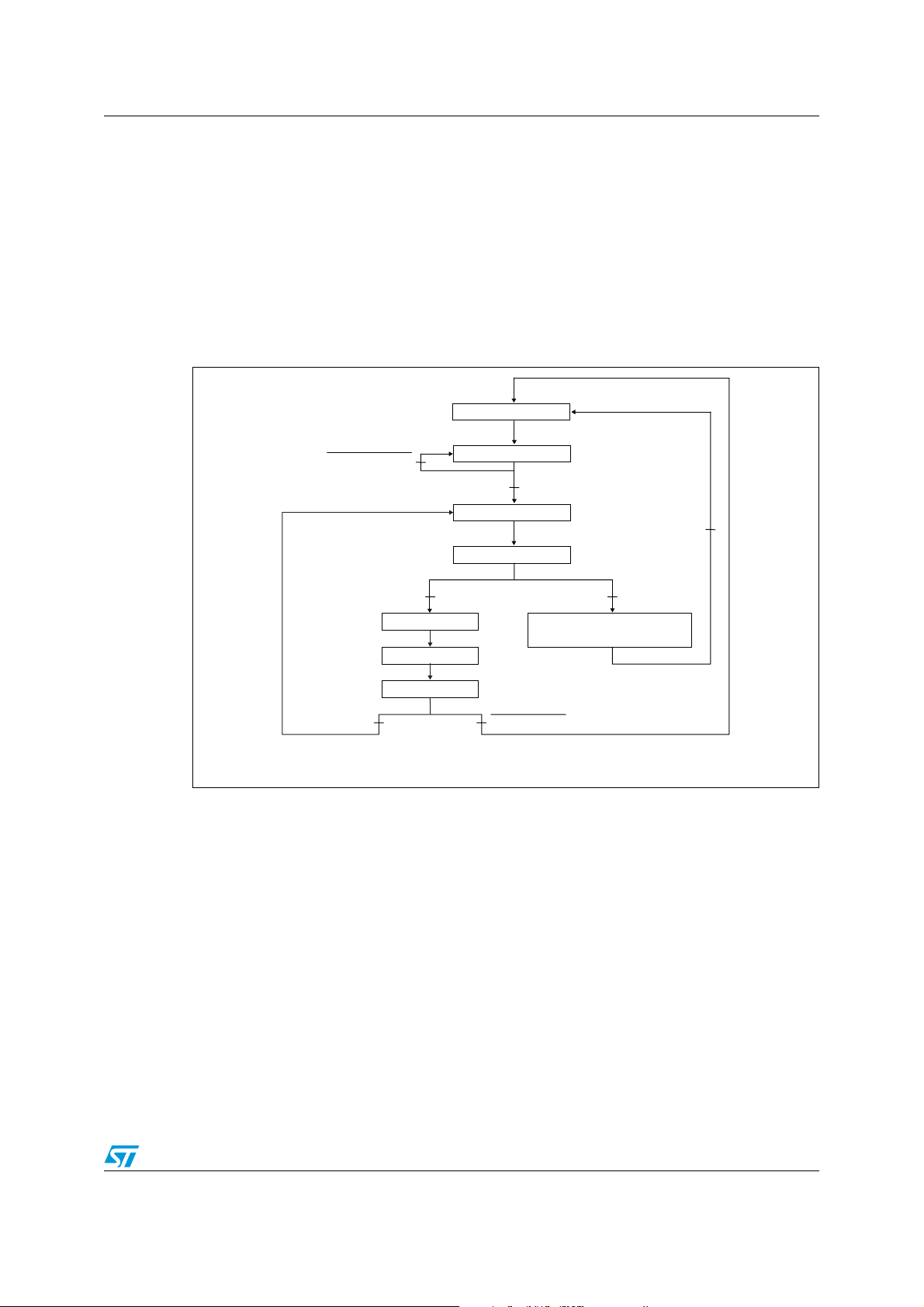
4.1.3 Control register CR1 - address 1
Amplifier output short-circuit detection: bits SC_L and SC_R
The amplifier’s outputs are protected from short-circuits that might accidentally occur during
manipulation of the device. In a typical application, if a short-circuit arises on the jack plug,
there will be no detection because of the serial resistor present on the amplifier output, thus
the output current threshold will not be reached.
To be active, the detection has to occur directly on the amplifier’s output with a signal
modulation on the inputs of the TS4621E. This detection is depicted in Figure 74.
Figure 74. Flowchart for short-circuit detection
Counter = 0
Shortcut detection
Counter < 3
Wait 40 ms
TS4621E power ON
Timeout = 40 ms
Shortcut detection
TS4621E power ON
Shortcut detection
Counter = counter + 1
TS4621E power OFF
Set flag SC_L or SC_R to 1
Set flag HiZ_L or HiZ_R to 1
Shortcut detection & timeout = 0
Reset
Counter = 3
AM06117
If a short-circuit is detected three consecutive times on one channel, a flag is raised in the
I²C read register CR1.
● SC_L: equals 0 during normal operation, equals 1 when a short-circuit is detected on
the left channel.
● SC_R: equals 0 during normal operation, equals 1 when a short-circuit is detected on
the right channel.
The corresponding channel’s output stage is then set to high impedance mode. An I²C read
command allows the reading of the SC_L and SC_R flags but does not reset them. An I²C
write command has to be sent to CR1 to reset the flags to 0 and restore normal operation.
Doc ID 022201 Rev 1 25/32

Application information TS4621E
Thermal shutdown protection: bit T_SH
A thermal shutdown protection is implemented to protect the device from overheating. If the
temperature rises above the thermal junction of 150°C, the device is put into standby mode
and a flag is raised in the read register CR1.
● T_SH: equals 0 during normal operation, equals 1 when a thermal shutdown is
detected.
When the temperature decreases to safe levels, the circuit switches back to normal
operation and the corresponding flag is cleared.
Software shutdown: bit SWS
When SWS equals 1, the device is set to I²C software shutdown. When SWS equals 0, the
negative supply and buck converters are activated.
Channel activation: bits HP_EN_L and HP_EN_R
When HP_EN_L or HP_EN_R equals 1, the corresponding amplifier channel is enabled.
4.2 Wake-up and standby time definition
The wake-up time of the TS4621E is guaranteed at 12 ms typical (refer to Chapter 3:
Electrical characteristics on page 7). However, since the TS4621E is activated with an I
bus, the wake-up start procedure is as follows.
1. The master sends a start bit.
2. The master sends the device address.
3. The slave (TS4621E) answers by an acknowledge bit.
4. The master sends the register address.
5. The slave (TS4621E) answers by an acknowledge bit.
6. The master sends the output mode configuration (CR1).
7. If the TS4621E was previously in standby mode, the wake-up starts on the falling edge
of the eighth clock signal (SCL) corresponding to the CR1 byte.
8. After 12 ms (de-pop sequence time), the TS4621E outputs are operational.
The standby time is guaranteed as 100 µs typical (refer to Chapter 3: Electrical
characteristics on page 7). However, since the TS4621E is de-activated with an I
standby time operates as follows.
1. The master sends a start bit.
2. The master sends the device address.
3. The slave (TS4621E) answers by an acknowledge bit.
4. The master sends the register address.
5. The slave (TS4621E) answers by an acknowledge bit.
6. The master sends the output mode configuration (CR1), which corresponds, in this
case, to standby mode.
7. The standby time starts on the falling edge of the eighth clock signal (SCL)
corresponding to the CR1 byte.
8. After 100 µs, the TS4621E is in standby mode.
2
2
C
C bus, the
26/32 Doc ID 022201 Rev 1

TS4621E Application information
4.3 Common mode sense
The TS4621E implements a common-mode sense pin to correct any voltage differences
that might occur between the return of the headphone jack and the GND of the device and
create parasitic noise in the headphone and/or line out.
The solution to strongly reduce and practically eliminate this noise consists in connecting
the headphone jack ground to the CMS pin. This pin senses the difference of potential
(voltage noise) between the TS4621E ground and the headphone ground. By way of the
frequency response of the common-mode sense pin, this noise is removed from the
TS4621E outputs.
Doc ID 022201 Rev 1 27/32
Package information TS4621E
k
5 Package information
In order to meet environmental requirements, ST offers these devices in different grades of
ECOPACK
specifications, grade definitions and product status are available at: www.st.com.
ECOPACK
®
packages, depending on their level of environmental compliance. ECOPACK®
®
is an ST trademark.
Figure 75. TS4621E footprint recommendation
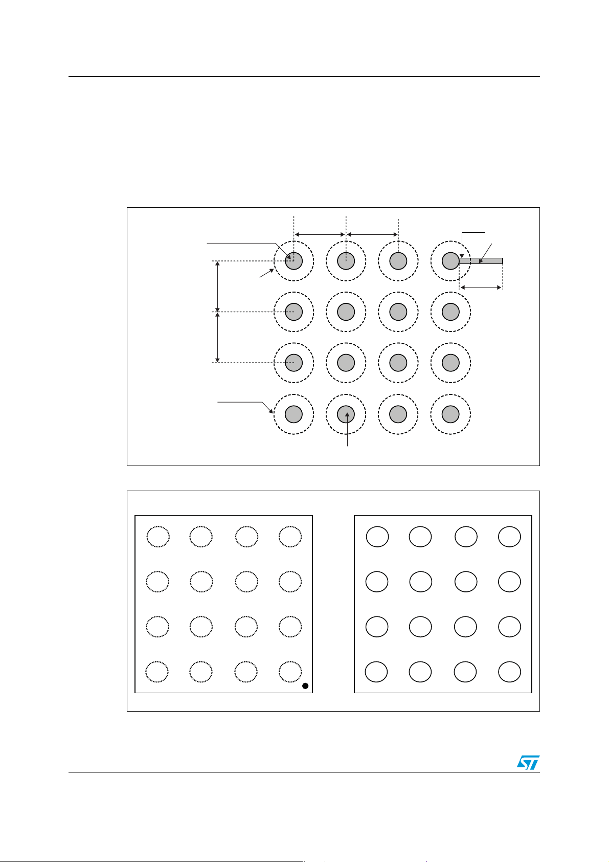
PCB pad size: Φ = 260 µm maximum
Solder mask opening: Φ = 300 μm min
(for 260 µm diameter pad)
Φ = 220 µm recommended
Not soldered
mask opening
400 μm
400 μm
400 μm
400 μm
75 µm min.
100 μm max.
Trac
150 μm min.
Figure 76. Pinout
TOP VIEW (balls are underneath)
INR -
INR+
INL+
INL -
4 3 21
VOUTR
CMS
HPVDD
VOUTL
SCL
PVSS
C1
AVDD
Pad in Cu 18 μm with Flash NiAu (2-6 μm, 0.2 μm max.)
BOTTOM VIEW
SDA
C2
AGND
SW
D
D
C
B
A
SDA
C2
C
AGND
B
SW
A
123 4
SCL
PVSS
C1
AVDD
VOUTR
CMS
HPVDD
VOUTL
INR -
INR+
INL+
INL -
28/32 Doc ID 022201 Rev 1

TS4621E Package information
Figure 77. Marking (top view)
■ Logo: ST
■ Symbol for lead-free: E
■ Part number: 21
■ X digit: Assembly code
■ Date code: YWW
■ The dot marks pin A1
Figure 78. Flip-chip - 16 bumps
1650 μm
400 μm
400 μm
1650 μm
E
E
21X
21X
YWW
YWW
■ Die size: 1.65 mm x 1.65 mm ± 30 µm
■ Die height (including bumps): 600 µm
±55 µm
■ Bump diameter: 250 µm ±40 µm
■ Bump height: 205 µm ±35 µm
■ Die height: 395 µm ±20 µm
■ Pitch: 400 µm ±40 µm
■ Coplanarity: 50 µm max
600 μm
Figure 79. Device orientation in tape pocket
4
1
A
8
Die size Y + 70 µm
Die size X + 70 µm
4
All dimensions are in mm
User direction of feed
1.5
1
A
Doc ID 022201 Rev 1 29/32

Ordering information TS4621E
6 Ordering information
Table 12. Order codes
Order code Temperature range Package Packing Marking
TS4621EIJT -40°C to +85°C Flip-chip Tape & reel 21
30/32 Doc ID 022201 Rev 1

TS4621E Revision history
7 Revision history
Table 13. Document revision history
Date Revision Changes
06-Sep-2011 1 Initial release.
Doc ID 022201 Rev 1 31/32

TS4621E
Please Read Carefully:
Information in this document is provided solely in connection with ST products. STMicroelectronics NV and its subsidiaries (“ST”) reserve the
right to make changes, corrections, modifications or improvements, to this document, and the products and services described herein at any
time, without notice.
All ST products are sold pursuant to ST’s terms and conditions of sale.
Purchasers are solely responsible for the choice, selection and use of the ST products and services described herein, and ST assumes no
liability whatsoever relating to the choice, selection or use of the ST products and services described herein.
No license, express or implied, by estoppel or otherwise, to any intellectual property rights is granted under this document. If any part of this
document refers to any third party products or services it shall not be deemed a license grant by ST for the use of such third party products
or services, or any intellectual property contained therein or considered as a warranty covering the use in any manner whatsoever of such
third party products or services or any intellectual property contained therein.
UNLESS OTHERWISE SET FORTH IN ST’S TERMS AND CONDITIONS OF SALE ST DISCLAIMS ANY EXPRESS OR IMPLIED
WARRANTY WITH RESPECT TO THE USE AND/OR SALE OF ST PRODUCTS INCLUDING WITHOUT LIMITATION IMPLIED
WARRANTIES OF MERCHANTABILITY, FITNESS FOR A PARTICULAR PURPOSE (AND THEIR EQUIVALENTS UNDER THE LAWS
OF ANY JURISDICTION), OR INFRINGEMENT OF ANY PATENT, COPYRIGHT OR OTHER INTELLECTUAL PROPERTY RIGHT.
UNLESS EXPRESSLY APPROVED IN WRITING BY TWO AUTHORIZED ST REPRESENTATIVES, ST PRODUCTS ARE NOT
RECOMMENDED, AUTHORIZED OR WARRANTED FOR USE IN MILITARY, AIR CRAFT, SPACE, LIFE SAVING, OR LIFE SUSTAINING
APPLICATIONS, NOR IN PRODUCTS OR SYSTEMS WHERE FAILURE OR MALFUNCTION MAY RESULT IN PERSONAL INJURY,
DEATH, OR SEVERE PROPERTY OR ENVIRONMENTAL DAMAGE. ST PRODUCTS WHICH ARE NOT SPECIFIED AS "AUTOMOTIVE
GRADE" MAY ONLY BE USED IN AUTOMOTIVE APPLICATIONS AT USER’S OWN RISK.
Resale of ST products with provisions different from the statements and/or technical features set forth in this document shall immediately void
any warranty granted by ST for the ST product or service described herein and shall not create or extend in any manner whatsoever, any
liability of ST.
ST and the ST logo are trademarks or registered trademarks of ST in various countries.
Information in this document supersedes and replaces all information previously supplied.
The ST logo is a registered trademark of STMicroelectronics. All other names are the property of their respective owners.
© 2011 STMicroelectronics - All rights reserved
STMicroelectronics group of companies
Australia - Belgium - Brazil - Canada - China - Czech Republic - Finland - France - Germany - Hong Kong - India - Israel - Italy - Japan -
Malaysia - Malta - Morocco - Philippines - Singapore - Spain - Sweden - Switzerland - United Kingdom - United States of America
www.st.com
32/32 Doc ID 022201 Rev 1
 Loading...