

Features
TS4601B
High performance stereo headphone amplifier
with capacitorless outputs and I
2
C bus interface
■ Power supply range: 2.9 V to 5.5 V
■ 107 dB of PSRR at 217 Hz
■ Fully differential inputs
■ I²C interface for volume control
■ Digital volume control range from -60 dB to
+4 dB
■ 101 dB of SNR A-weighted
■ Independent right and left channel shutdown
control
■ Low quiescent current: 4.8 mA typ. at 3.0 V
■ Low standby current: 2 µA max
■ Output-coupling capacitors removed
■ Flip-chip package 2.1 mm x 2.1 mm, 500 µm
pitch, 16 bumps
Applications
■ Cellular phones
■ Notebook computers
■ CD/MP3 players
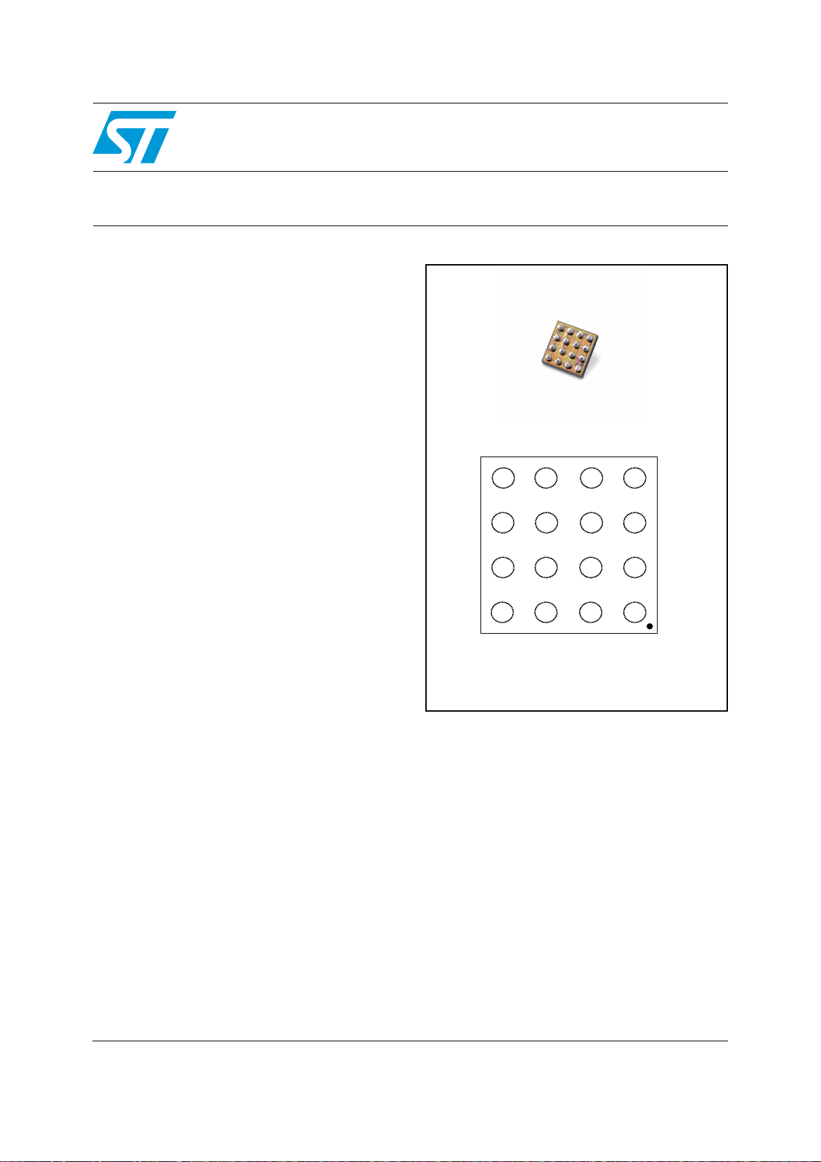
TS4601BEIJT - Flip-chip
Pinout (top view)
SDA
SDZ
SDZ
INR-
INR-
INL-
INL-
SDA
INR+
INR+
INL+
INL+
GND
GND
4321
4321
SCL
SCL
CMS
CMS
PVSS
PVSS
C1
C1
VOUTR
VOUTR
VCC
VCC
VOUTL
VOUTL
C2PVCC
C2PVCC
D
D
C
C
B
B
A
A
Balls are underneath
Description
The TS4601B is a stereo headphone driver
dedicated to high audio performance and spaceconstrained applications. It has the same uses as
the TS4601 which it replaces, while offering highly
improved ESD ratings.
It is based on low power dissipation amplifier core
technology. Special care was taken in the design
of the amplification chain to achieve peerless
PSRR (107 dB typ. at 217 Hz) and 101 dB of
SNR.
The TS4601B can drive 0.9 V
into 16 Ω and 1.6 V
into 10 kΩ, whatever the
rms
output voltage
rms
An I²C interface offers volume control in 64 steps
from -60 dB to +4 dB and multiple configuration
modes for the device.
The traditionally used output-coupling capacitors
can be removed and a dedicated common-mode
sense pin removes parasitic noise from the jack.
The TS4601B is designed to be used with an
output serial resistor. It ensures unconditional
stability over a wide range of capacitive loads.
The TS4601B is packaged in a tiny 16-bump flipchip with a pitch of 500 µm and a 300 µm
diameter ball size.
power supply voltage, in the 2.9 V to 5.5 V range.
July 2008 Rev 2 1/28
www.st.com
28

Contents TS4601B
Contents
1 Absolute maximum ratings and operating conditions . . . . . . . . . . . . . 3
2 Typical application schematics . . . . . . . . . . . . . . . . . . . . . . . . . . . . . . . . 4
3 Electrical characteristics . . . . . . . . . . . . . . . . . . . . . . . . . . . . . . . . . . . . . 6
3.1 Electrical characteristics tables . . . . . . . . . . . . . . . . . . . . . . . . . . . . . . . . . 6
3.2 Electrical characteristic curves . . . . . . . . . . . . . . . . . . . . . . . . . . . . . . . . . . 8
4 Application information . . . . . . . . . . . . . . . . . . . . . . . . . . . . . . . . . . . . . 17
4.1 Common-mode sense . . . . . . . . . . . . . . . . . . . . . . . . . . . . . . . . . . . . . . . 17
4.2 I²C bus interface . . . . . . . . . . . . . . . . . . . . . . . . . . . . . . . . . . . . . . . . . . . . 17
4.2.1 I²C bus operation . . . . . . . . . . . . . . . . . . . . . . . . . . . . . . . . . . . . . . . . . . 17
4.2.2 Control registers . . . . . . . . . . . . . . . . . . . . . . . . . . . . . . . . . . . . . . . . . . 19
Control register CR0 . . . . . . . . . . . . . . . . . . . . . . . . . . . . . . . . . . . . . . . . . . . . . . . 21
4.3 Wake-up and standby time definition . . . . . . . . . . . . . . . . . . . . . . . . . . . . 22
4.4 Decoupling considerations . . . . . . . . . . . . . . . . . . . . . . . . . . . . . . . . . . . . 22
4.5 Low frequency response . . . . . . . . . . . . . . . . . . . . . . . . . . . . . . . . . . . . . 23
4.6 Low pass output filter . . . . . . . . . . . . . . . . . . . . . . . . . . . . . . . . . . . . . . . . 23
4.7 Single-ended input configuration . . . . . . . . . . . . . . . . . . . . . . . . . . . . . . . 24
5 Package information . . . . . . . . . . . . . . . . . . . . . . . . . . . . . . . . . . . . . . . . 25
6 Ordering information . . . . . . . . . . . . . . . . . . . . . . . . . . . . . . . . . . . . . . . 27
7 Revision history . . . . . . . . . . . . . . . . . . . . . . . . . . . . . . . . . . . . . . . . . . . 27
2/28
TS4601B Absolute maximum ratings and operating conditions
1 Absolute maximum ratings and operating conditions
Table 1. Absolute maximum ratings
Symbol Parameter Value Unit
V
CC
Supply voltage
Input voltage
V
in
In Master standby mode, and I²C mode 1, 6
and 7
In I²C mode 2, 3, 4 and 5
T
stg
T
R
thja
P
d
Storage temperature -65 to +150 °C
Maximum junction temperature 150 °C
j
Thermal resistance junction to ambient
Power dissipation Internally limited
HBM - human body model - all pins
VOUTL, VOUTR vs. VCC, GND
MM - machine model (min. value)
ESD
CDM - charge device model 500 V
IEC61000-4-2 level 4, contact
IEC61000-4-2 level 4, air discharge
Latch-up Latch-up immunity 200 mA
Lead temperature (soldering, 10sec) 260 °C
(1)
(6)
(5)
(4)
(6)
(2)
6V
0 to V
CC
V
-2.4 to +2.4
200 °C/W
(3)
2
4
kV
200 V
+/- 8
+/- 15
kV
1. All voltage values are measured with respect to the ground pin.
2. The device is protected in case of over temperature by a thermal shutdown active @ 150° C.
3. Exceeding the power derating curves during a long period may provoke abnormal operation.
4. Human body model: A 100 pF capacitor is charged to the specified voltage, then discharged through a
1.5 kΩ resistor between two pins of the device. This is done for all couples of connected pin combinations
while the other pins are floating.
5. Machine model: A 200 pF capacitor is charged to the specified voltage, then discharged directly between
two pins of the device with no external series resistor (internal resistor < 5 Ω). This is done for all couples of
connected pin combinations while the other pins are floating.
6. The measurement is performed on the evaluation board, with an STMicroelectronics ESD protection
EMIF02-AV01F3
Table 2. Operating conditions
Symbol Parameter Value Unit
V
T
R
CC
R
C
oper
thja
Supply voltage 2.9 to 5.5 V
Load resistor ≥ 16 Ω
L
L
Load capacitor
Serial resistor of 12Ω minimum, R
≥ 16Ω,
L
0.8 to 100 nF
Operating free air temperature range -40 to +85 °C
Flip-chip thermal resistance junction to ambient 90 °C/W
3/28
Typical application schematics TS4601B
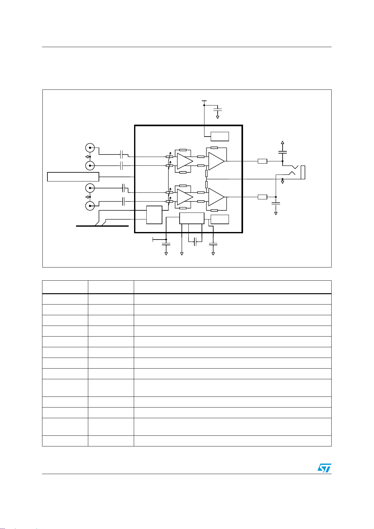
2 Typical application schematics
Figure 1. Typical application schematics for the TS4601B
Vcc
Cs
1uF
Vcc
Gnd
C1
Positive
Reg
-
+
+
-
Negative
Reg
PVss
B2
Css
2.2uF
VoutL
CMS
VoutR
12 ohms min.
B1
C2
12 ohms min.
D1
Rout
Rout
Gnd
Gnd
Gnd
Cout
0.8nF min.
Cout
0.8nF min.
Headphone / Line Out
Negative Left Input
Gnd
Positive Left Input
Master Standby Command
Positive Right Input
Gnd
Negative Right Input
I2C Bus
Cin
2.2uF
Cin
2.2uF
Cin
2.2uF
Cin
2.2uF
B4
B3
D4
C3
C4
D3
D2
TS4601
InL-
InL+
SDZ
InR+
InR-
SDA
SCL
-
+
+
-
I2C
PVcc Gnd C1 C2
A4 A3 A2 A1
Vcc
Cs
1uF
Gnd GndGnd
Negative
Supply
C12
1uF
Table 3. Pin description for the TS4601B
Pin number Pin name Pin definition
C1 VCC Analog supply voltage, connect to V
A4 PVCC Power supply voltage, connect to V
battery
battery
A2 C1 Capacitor terminal for internal negative supply generator.
A1 C2 Capacitor terminal for internal negative supply generator.
B2 PVSS Capacitor terminal for internal negative supply generator filtering.
D1 VOUTR Right audio channel output signal.
B1 VOUTL Left audio channel output signal.
A3 GND Ground of the device.
C2 CMS
Common-mode sense, to be connected as close as possible to the ground of
headphone / line out plug.
B4 INL- Left audio channel negative input signal.
B3 INL+ Left audio channel positive input signal.
D4 SDZ
Master standby of the circuit. When SDZ = 0, the device is also reset to initial
state. Up to V
tolerant input.
CC
C4 INR- Right audio channel negative input signal.
.
.
4/28
TS4601B Typical application schematics
Table 3. Pin description for the TS4601B (continued)
Pin number Pin name Pin definition
C3 INR+ Right audio channel positive input signal.
D3 SDA I²C signal data. Up to V
D2 SCL I²C clock signal. Up to V
tolerant input.
CC
tolerant input.
CC
Table 4. Component description for the TS4601B
Component Value Description
and PVCC. Two 1µF capacitors are enough for
CC
Cs 1µF
C12 1µF
C
SS
C
in
C
out
R
out
2.2µF
Cin
------------------------=
2πZinFc
0.8nF to 100nF
12Ω min.
Decoupling capacitors for V
proper decoupling of TS4601B. X5R dielectric and 10V rating voltage is
recommended to minimize ΔC/ΔV when V
Must be placed as close as possible to the TS4601B to minimize parasitic
inductance and resistance.
Capacitor for internal negative power supply operation. X5R dielectric and 10V
rating voltage is recommended to minimize ΔC/ΔV when VCC=5V.
Must be placed as close as possible to the TS4601B to minimize parasitic
inductance and resistance.
Filtering capacitor for internal negative power supply. X5R dielectric and 10V
rating voltage is recommended to minimize ΔC/ΔV when V
1
Input coupling capacitor that forms with Zin, a first order high pass filter with a
-3dB cut-off frequency FC. Zin is 12kΩ typical and independent of the gain
setting.
For example F
= 13Hz, Cin = 1µF and for FC = 6Hz, Cin = 2.2µF
C
Output capacitor of 0.8nF minimum to 100nF maximum. This capacitor is
mandatory for operation of the TS4601B.
Output resistor in series with the TS4601B output. This 12Ω minimum resistor
is mandatory for operation of the TS4601B.
CC
=5V.
CC
= 5V.
5/28
Electrical characteristics TS4601B
3 Electrical characteristics
3.1 Electrical characteristics tables
Table 5. Electrical characteristics of the I²C interface
from V
=+2.9 V to VCC=+5.5 V, GND = 0 V, T
CC
= 25° C (unless otherwise specified)
amb
Symbol Parameter Min. Typ. Max. Unit
V
V
V
V
F
SCL
V
OL
I
in
Table 6. Electrical characteristics of the amplifier
Low level input voltage on SDZ pins 0.63 V
IL
High level input voltage on SDZ pins 1.1 V
IH
Low level input voltage on SDA, SCL pins 0.6 V
IL
High level input voltage on SDA, SCL pins 1.3 V
IH
I2C clock frequency 400 kHz
Low level output voltage, SDA pin, I
= 3mA 0.4 V
sink
Input current on SDA, SCL from 0.4V to 4.5V 10 µA
from V
=+2.9 V to VCC=+5.5 V, GND = 0 V, T
CC
= 25° C (unless otherwise specified)
amb
Symbol Parameter Min. Typ. Max. Unit
Quiescent supply current, no input signal, both channels
I
CC
enabled, RL= 16Ω
= 3.0V
V
CC
VCC = 5.0V
4.8
5.6
6
7
Master standby current, No input signal
I
STBY
I
STBY
= 0V
V
SDZ
V
= 0.35V, VCC= 5V
SDZ
0.5 2
10
I²C standby current, no input signal 75 µA
Pull-down resistor on SDZ 480 600 720 kΩ
V
V
oo
Input differential voltage range
in
Output offset voltage
No input signal, RL = 32Ω
(1)
1.2 V
-5 +5 mV
mA
µA
rms
Maximum output voltage, in-phase signals
V
out
Frequency
range
= 16Ω, THD+N = 1% max, f = 1kHz
R
L
= 10kΩ, Rs=15Ω, CL=1nF, THD+N = 1% max, f = 1kHz
R
L
RL = 16Ω, G = 0dB, P
= 20mW, +/- 0.5dB (related to1kHz)
out
Cin = 4.7µF
Total harmonic distortion + noise, G = 0dB
THD + N
R
= 16Ω, Po = 5mW, F = 1kHz
L
= 16Ω, Po = 10mW, 20Hz < F < 20kHz 0.2
R
L
6/28
0.9
V
1.6
10 22000 Hz
0.02 %
rms
TS4601B Electrical characteristics
Table 6. Electrical characteristics of the amplifier
from V
Symbol Parameter Min. Typ. Max. Unit
Power supply rejection ratio
F = 217Hz, R
PSRR
CMRR
Crosstalk
SNR
ONoise
G Gain range with Gain(dB) = 20xlog[(V
Mute InL/R+ - InL/R- = 1V
-
- Step size error -1 +1 stepsize
V
F = 10kHz, R
V
Common mode rejection ratio
= 16Ω, F = 20Hz to 20 kHz, G = 0dB, Vic = 200 mV
R
L
Channel separation
R
RL = 10kΩ, G = 0dB, F = 1kHz, V
Signal to noise ratio, A-weighted, R
THD+N < 1%, F = 1kHz, G=+4 dB
Output noise voltage, A-weighted
G= +4dB
G=-19.5dB -103
Gain step size
from -60dB to -36dB
from -36dB to -16.5dB
from -16.5dB to +4dB
Gain error (G = +4dB) -0.45 +0.42 dB
=+2.9 V to VCC=+5.5 V, GND = 0 V, T
CC
(2)
= 16Ω, G = 0dB
= 200mVpp, grounded inputs
ripple
= 200 mVpp, grounded inputs
ripple
= 16Ω, G = 0dB, F = 1kHz, Po = 40mW
L
L
= 16Ω, G = 0dB
L
rms
= 1.6V
out
=16 Ω, V
L
(3)
(3)
L/R)/(InL/R+ - InL/R-)] -60 +4 dB
out
rms
= 0.9V
out
= 25° C (unless otherwise specified)
amb
100
107
70
65 dB
pp
60
80
rms
82
84
101 dB
-100
-80 dB
3
1.5
0.5
dB
dB
dBV
dB
Left and right channel input impedance all gains setting
Z
in
Single-ended inputs referenced to GND
Differential inputs
Output impedance in Mode 5 (negative supply is ON and
amplifier output stages are OFF)
Z
out
F < 40kHz
F = 6MHz
F = 36MHz
t
wu
t
STBY
1. Guaranteed by design and parameter correlation.
2. Dynamic measurements - 20*log(rms(V
3. Guaranteed by design and parameter correlation.
Wake-up time 12 22 ms
Standby time 10 µs
)/rms(V
out
(3)
ripple
10
20
12
24
14.5
29
10
500
75
)). V
is an added sinus signal to VCC @ F = 217 Hz.
ripple
7/28
kΩ
kΩ
Ω
Ω

Electrical characteristics TS4601B
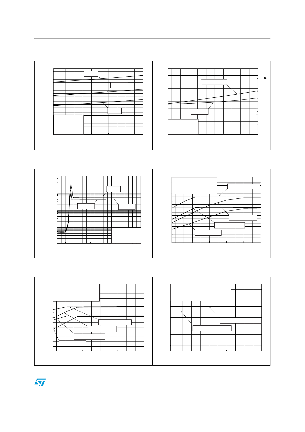
3.2 Electrical characteristic curves
Current consumption vs. power supply voltage see Figure 2
Standby current consumption vs. power supply voltage see Figure 3 and Figure 4
Maximum output power vs. power supply voltage see Figure 5
Maximum output power vs. power supply voltage see Figure 6
Maximum output voltage vs. power supply voltage see Figure 7
PSRR vs. frequency see Figure 8 to Figure 12
PSRR vs. gain setting see Figure 13
THD+N vs. output power see Figure 14 to Figure 25
THD+N vs. output voltage see Figure 26
THD+N vs. frequency see Figure 27
THD+N vs. frequency see Figure 28 to Figure 39
CMRR vs. frequency see Figure 40 and Figure 41
Crosstalk vs. frequency see Figure 42 to Figure 45
Common mode response vs. frequency see Figure 46
THD+N vs. input voltage. Line in mode 5 see Figure 47
Input impedance vs. frequency. Line in mode 5 see Figure 48
Gain vs. frequency see Figure 49
Note: When the label “RC network” is present in a curve, it means that a 12 Ω + 1 nF low pass filter
connected on outputs is used (refer to Figure 1: Typical application schematics for the
TS4601B on page 4).
8/28
TS4601B Electrical characteristics
3.0 3.5 4.0 4.5 5.0 5.5
0
25
50
75
100
125
150
175
200
225
250
275
300
THD+N=10% (180°)
THD+N=10% (0°)
THD+N=1% (0°)
RL = 16Ω, F = 1kHz
Left & Right
BW < 30kHz, Tamb = 25°C
THD+N=1% (180°)
Output power (mW)
Vcc (V)
3.0 3.5 4.0 4.5 5.0 5.5
0.0
0.5
1.0
1.5
2.0
2.5
3.0
THD+N=10% (0° & 180°)
RL = RC network + 10kΩ, F = 1kHz
Left & Right
BW < 30kHz, Tamb = 25°C
THD+N=1% (0° & 180°)
Output Voltage (Vrms)
Vcc (V)
Figure 2. Current consumption vs. power
supply voltage
6.0
5.5
5.0
4.5
4.0
3.5
3.0
2.5
2.0
1.5
No load
Current Consumption (mA)
SDZ = Vcc
1.0
SDA = SCL = Vcc
0.5
Ta = 25°C
0.0
3.0 3.5 4.0 4.5 5.0 5.5
Mode 4
Mode 2, 3
Mode 5
Power Supply Voltage (V)
Figure 4. Standby current consumption vs.
standby voltage
1E-3
1E-4
Vcc=5V
Figure 3. Standby current consumption vs.
power supply voltage
1000
800
600
400
200
No load
SDA = SCL = Vcc
Current Consumption SDZ=Gnd (nA)
Ta = 25°C
0
3.0 3.5 4.0 4.5 5.0 5.5
Mode 1, 6, 7, 8
SDZ=Gnd
Power Supply Voltage (V)
100
90
80
70
60
50
40
30
20
10
0
Figure 5. Maximum output power vs. power
supply voltage
Current Consumption SDZ=Vcc ( A)
1E-5
1E-6
Current Consumption (nA)
1E-7
0.0 0.5 1.0 1.5 2.0 2.5 3.0 3.5 4.0 4.5 5.0
Vcc=2.9V
Figure 6. Maximum output power vs. power
supply voltage
175
RL = 32Ω, F = 1kHz
Left & Right
150
BW < 30kHz, Tamb = 25°C
125
100
75
50
Output power (mW)
25
0
3.0 3.5 4.0 4.5 5.0 5.5
THD+N=1% (180°)
THD+N=1% (0°)
SDZ Voltage (V)
THD+N=10% (180°)
THD+N=10% (0°)
Vcc (V)
Vcc=3.6V
No load
SDA = SCL = Vcc
Ta = 25°C
Figure 7. Maximum output voltage vs. power
supply voltage
9/28

Electrical characteristics TS4601B
100 1000 10000
-130
-120
-110
-100
-90
-80
-70
-60
-50
-40
-30
-20
-10
0
20k
20
Vcc=5V
Vcc=3.6V
Vcc=2.9V
Vripple = 200mVpp
G = 4dB
Inputs = grounded
Left & Right
RL = RC network + 16
Ω
Tamb = 25°C
PSRR (dB)
Frequency (Hz)
100 1000 10000
-130
-120
-110
-100
-90
-80
-70
-60
-50
-40
-30
-20
-10
0
20k
20
Vcc=5V
Vcc=3.6V
Vcc=2.9V
Vripple = 200mVpp
G = 4dB
Inputs = grounded
Left & Right
RL = RC network + 32
Ω
Tamb = 25°C
PSRR (dB)
Frequency (Hz)
Figure 8. PSRR vs. frequency Figure 9. PSRR vs. frequency
0
-10
Vripple = 200mVpp
G = 4dB
-20
Inputs = grounded
-30
Left & Right
-40
RL = 16
-50
-60
-70
PSRR (dB)
Ω
Tamb = 25°C
Vcc=2.9V
-80
-90
-100
-110
-120
20
100 1000 10000
Frequency (Hz)
Vcc=3.6V
Vcc=5V
20k
Figure 10. PSRR vs. frequency Figure 11. PSRR vs. frequency
0
-10
Vripple = 200mVpp
G = 4dB
-20
Inputs = grounded
-30
Left & Right
-40
RL = 32
Ω
Tamb = 25°C
100 1000 10000
Vcc=2.9V
Frequency (Hz)
Vcc=3.6V
Vcc=5V
20k
PSRR (dB)
-50
-60
-70
-80
-90
-100
-110
-120
20
Figure 12. PSRR vs. frequency Figure 13. PSRR vs. gain setting
0
-10
Vripple = 200mVpp
G = 4dB
-20
Inputs = grounded
-30
Left & Right
-40
RL = RC network + 10k
-50
Tamb = 25°C
-60
-70
PSRR (dB)
Ω
Vcc=2.9V
-80
-90
-100
-110
-120
20
100 1000 10000
Frequency (Hz)
Vcc=3.6V
Vcc=5V
20k
10/28
0
Vripple = 200mVpp
F = 217Hz
-20
RL ≥ 16
Ω
Vcc = 2.9V to 5.5V
Ta = 25°C
-40
-60
PSRR (dB)
-80
Left & Right
-100
-120
-80 -60 -40 -20 0
Gain setting (dB)
4

TS4601B Electrical characteristics
Figure 14. THD+N vs. output power Figure 15. THD+N vs. output power
10
RL = 16
Ω
Vcc = 5V
G = 4dB
Inputs = 0
1
°
Left & Right
BW < 30kHz
F=8kHz
F=1kHz
THD+N (%)
0.01
0.1
Tamb = 25°C
F=80Hz
1 10 100
Output Power (mW)
10
RL = 16
Ω
Vcc = 5V
G = 4dB
Inputs = 180
1
°
Left & Right
BW < 30kHz
F=8kHz
F=1kHz
THD+N (%)
0.1
Tamb = 25°C
F=80Hz
0.01
1 10 100
Output Power (mW)
Figure 16. THD+N vs. output power Figure 17. THD+N vs. output power
10
1
THD+N (%)
0.1
RL = 16
Ω
Vcc = 3.6V
G = 4dB
Inputs = 0
°
Left & Right
BW < 30kHz
Tamb = 25°C
F=80Hz
F=8kHz
10
1
THD+N (%)
0.1
RL = 16
Ω
Vcc = 3.6V
G = 4dB
Inputs = 180
Left & Right
BW < 30kHz
Tamb = 25°C
°
F=8kHz
F=1kHz
0.01
F=1kHz
1 10 100
Output Power (mW)
0.01
1 10 100
Output Power (mW)
Figure 18. THD+N vs. output power Figure 19. THD+N vs. output power
10
RL = 16
Ω
Vcc = 2.9V
G = 4dB
Inputs = 0
1
Left & Right
°
F=8kHz
BW < 30kHz
Tamb = 25°C
THD+N (%)
0.1
0.01
F=1kHz
1 10 100
Output Power (mW)
F=80Hz
11/28
10
RL = 16
Ω
Vcc = 2.9V
G = 4dB
1
0.1
THD+N (%)
Inputs = 180
Left & Right
BW < 30kHz
Tamb = 25°C
°
F=8kHz
F=1kHz
0.01
1 10 100
Output Power (mW)
F=80Hz
F=80Hz

Electrical characteristics TS4601B
Figure 20. THD+N vs. output power Figure 21. THD+N vs. output power
10
RL = 32
Ω
Vcc = 5V
G = 4dB
Inputs = 0
1
°
Left & Right
THD+N (%)
0.01
0.1
BW < 30kHz
Tamb = 25°C
F=8kHz
F=1kHz
F=80Hz
1 10 100
Output Power (mW)
10
RL = 32
Ω
Vcc = 5V
G = 4dB
1
Inputs = 180
°
Left & Right
THD+N (%)
0.1
BW < 30kHz
Tamb = 25°C
F=8kHz
F=1kHz
0.01
1 10 100
Output Power (mW)
F=80Hz
Figure 22. THD+N vs. output power Figure 23. THD+N vs. output power
10
1
THD+N (%)
0.1
RL = 32
Ω
Vcc = 3.6V
G = 4dB
Inputs = 0
°
Left & Right
BW < 30kHz
Tamb = 25°C
F=8kHz
F=1kHz
10
1
THD+N (%)
0.1
RL = 32
Ω
Vcc = 3.6V
G = 4dB
Inputs = 180
Left & Right
BW < 30kHz
Tamb = 25°C
°
F=8kHz
F=1kHz
0.01
F=80Hz
1 10 100
Output Power (mW)
0.01
1 10 100
Output Power (mW)
Figure 24. THD+N vs. output power Figure 25. THD+N vs. output power
10
RL = 32
Ω
Vcc = 2.9V
G = 4dB
THD+N (%)
0.1
0.01
1
Inputs = 0
Left & Right
BW < 30kHz
Tamb = 25°C
°
F=8kHz
F=1kHz
F=80Hz
1 10 100
Output Power (mW)
10
RL = 32
Ω
Vcc = 2.9V
G = 4dB
THD+N (%)
0.1
0.01
1
Inputs = 180
Left & Right
BW < 30kHz
Tamb = 25°C
°
F=8kHz
F=1kHz
F=80Hz
1 10 100
Output Power (mW)
F=80Hz
12/28

TS4601B Electrical characteristics
100 1000 10000
0.01
0.1
1
Vo=1.5Vrms
Vo=400mVrms
Vo=30mVrms
RL = RC network + 10k
Ω
Vcc = 2.9V to 5.5V
G = 4dB
Inputs = 0° & 180
°
Left & Right
Bw < 30kHz
Tamb = 25°C
20k20
THD + N (%)
Frequency (Hz)
100 1000 10000
0.01
0.1
1
Po=70mW
Po=10mW
RL = 16Ω
Vcc = 5V, G = 4dB
Inputs = 180°
Left & Right
Bw < 30kHz
Tamb = 25°C
20k20
THD + N (%)
Frequency (Hz)
100 1000 10000
0.01
0.1
1
Po=70mW
Po=10mW
RL = 16Ω
Vcc = 3.6V, G = 4dB
Inputs = 180°
Left & Right
Bw < 30kHz
Tamb = 25°C
20k20
THD + N (%)
Frequency (Hz)
Figure 26. THD+N vs. output voltage Figure 27. THD+N vs. frequency
10
RL = RC network + 10k
Ω
Vcc = 2.9V to 5.5V, G = 4dB
Inputs = 0° & 180
1
Left & Right
BW < 30kHz, Tamb = 25°C
0.1
THD+N (%)
°
F=1kHz
F=8kHz
0.01
F=80Hz
1E-3
10 100 1000
Output Voltage (mVrms)
Figure 28. THD+N vs. frequency Figure 29. THD+N vs. frequency
1
RL = 16Ω
Vcc = 5V, G = 4dB
Inputs = 0°
Left & Right
Bw < 30kHz
0.1
Tamb = 25°C
Po=70mW
THD + N (%)
0.01
100 1000 10000
Frequency (Hz)
Po=10mW
20k20
Figure 30. THD+N vs. frequency Figure 31. THD+N vs. frequency
1
RL = 16Ω
Vcc = 3.6V, G = 4dB
Inputs = 0°
0.1
THD + N (%)
0.01
Left & Right
Bw < 30kHz
Tamb = 25°C
100 1000 10000
Po=70mW
Po=10mW
20k20
Frequency (Hz)
13/28

Electrical characteristics TS4601B
100 1000 10000
0.01
0.1
1
Po=50mW
Po=10mW
RL = 16Ω
Vcc = 2.9V
G = 4dB
Inputs = 180°
Left & Right
Bw < 30kHz
Tamb = 25°C
20k20
THD + N (%)
Frequency (Hz)
100 1000 10000
0.01
0.1
1
Po=60mW
Po=10mW
RL = 32Ω
Vcc = 5V
G = 4dB
Inputs = 180°
Left & Right
Bw < 30kHz
Tamb = 25°C
20k20
THD + N (%)
Frequency (Hz)
100 1000 10000
0.01
0.1
1
Po=60mW
Po=10mW
RL = 32Ω
Vcc = 3.6V
G = 4dB
Inputs = 180°
Left & Right
Bw < 30kHz
Tamb = 25°C
20k20
THD + N (%)
Frequency (Hz)
Figure 32. THD+N vs. frequency Figure 33. THD+N vs. frequency
1
RL = 16Ω
Vcc = 2.9V
G = 4dB
Inputs = 0°
Po=50mW
Left & Right
Bw < 30kHz
0.1
Tamb = 25°C
THD + N (%)
Po=10mW
0.01
100 1000 10000
Frequency (Hz)
20k20
Figure 34. THD+N vs. frequency Figure 35. THD+N vs. frequency
1
RL = 32Ω
Vcc = 5V
G = 4dB
Inputs = 0°
0.1
THD + N (%)
Left & Right
Bw < 30kHz
Tamb = 25°C
Po=60mW
14/28
0.01
100 1000 10000
Frequency (Hz)
Po=10mW
20k20
Figure 36. THD+N vs. frequency Figure 37. THD+N vs. frequency
1
RL = 32Ω
Vcc = 3.6V
G = 4dB
Inputs = 0°
0.1
THD + N (%)
0.01
Left & Right
Bw < 30kHz
Tamb = 25°C
100 1000 10000
Po=60mW
Po=10mW
20k20
Frequency (Hz)

TS4601B Electrical characteristics
100 1000 10000
0.01
0.1
1
Po=50mW
Po=10mW
RL = 32Ω
Vcc = 2.9V
G = 4dB
Inputs = 0°
Left & Right
Bw < 30kHz
Tamb = 25°C
20k20
THD + N (%)
Frequency (Hz)
100 1000 10000
-80
-70
-60
-50
-40
-30
-20
-10
0
20k
20
Vcc=2.9V to 5.5V
Δ
Vic = 200mVpp
G = 0dB
Left & Right
RL ≥ 16
Ω
Tamb = 25°C
CMRR (dB)
Frequency (Hz)
100 1000 10000
0
10
20
30
40
50
60
70
80
90
100
Right to Left
20k
20
Left to Right
G = 4dB
Vcc = 3.6V
Pout = 40mW
RL = 16
Ω
Tamb = 25°C
Crosstalk (dB)
Frequency (Hz)
Figure 38. THD+N vs. frequency Figure 39. THD+N vs. frequency
1
RL = 32Ω
Vcc = 2.9V
G = 4dB
Inputs = 0°
0.1
THD + N (%)
0.01
Left & Right
Bw < 30kHz
Tamb = 25°C
100 1000 10000
Po=50mW
Po=10mW
20k20
Frequency (Hz)
Figure 40. CMRR vs. frequency Figure 41. CMRR vs. frequency
0
Δ
Vic = 200mVpp
-10
G = 4dB
Left & Right
-20
RL ≥ 16
Ω
Tamb = 25°C
-30
CMRR (dB)
-40
-50
-60
-70
-80
20
Vcc=2.9V to 5.5V
100 1000 10000
Frequency (Hz)
20k
Figure 42. Crosstalk vs. frequency Figure 43. Crosstalk vs. frequency
100
90
80
70
Left to Right
60
50
40
Crosstalk (dB)
G = 4dB
30
Vcc = 5V
Pout = 40mW
20
RL = 16
10
0
20
Ω
Tamb = 25°C
Right to Left
100 1000 10000
Frequency (Hz)
20k
15/28

Electrical characteristics TS4601B
100 1000 10000
0
10
20
30
40
50
60
70
80
90
100
Right to Left
20k
20
Left to Right
G = 4dB
Vcc = 2.9V to 5.5V
Vout = 1.6Vrms
RL = RC network + 10k
Ω
Tamb = 25°C
Crosstalk (dB)
Frequency (Hz)
1E-3 0.01 0.1 1
1E-4
1E-3
0.01
0.1
1
10
Reference F=80Hz, 1kHz, 8kHz
Line In F=80Hz, 1kHz, 8kHz
Mode 5
Vcc = 2.9V to 5.5V
Zout generator = 1k
Ω
BW < 30kHz, Tamb = 25°C
THD+N (%)
Input Voltage (Vrms)
Figure 44. Crosstalk vs. frequency Figure 45. Crosstalk vs. frequency
100
90
80
70
Left to Right
60
50
40
Crosstalk (dB)
G = 4dB
30
Vcc = 2.9V
Pout = 40mW
20
RL = 16
10
Tamb = 25°C
0
20
Figure 46. Common mode response vs.
frequency
0
V
= 20mVrms
CMS
-10
G = All gains
Left & Right
-20
(dB)
RL ≥ 16
CMS
Tamb = 25°C
-30
/V
out
-40
-50
-60
-70
CMS response : V
-80
20
Right to Left
Ω
100 1000 10000
Ω
100 1000 10000
Frequency (Hz)
Vcc=2.9V to 5.5V
Frequency (Hz)
20k
Figure 47. THD+N vs. input voltage. Line in
mode 5
20k
Figure 48. Input impedance vs. frequency.
Line in mode 5
10
1
Zin from outputs (k )
0.1
0.1 1 10 100 1000 10000
16/28
Frequency (kHz)
Mode 5
Vcc = 2.9V to 5.5V
Vin = 1Vrms
Tamb = 25°C
Figure 49. Gain vs. frequency
4
2
0
-2
-4
Gain(dB)
Vcc = 2.9V to 5.5V
G = 0dB
-6
Cin = 4.7μF
Left & Right
-8
Tamb = 25°C
-10
10 100 1000 10000 100000
RL=RC network+10kΩ, Vo=1Vrms
RL=16Ω, Po=20mW
Frequency (Hz)

TS4601B Application information
4 Application information
4.1 Common-mode sense
The TS4601B implements a common-mode sense to correct the voltage differences that
might occur between the headphone jack return and the GND of the device, thus creating
parasitic noise in the headphone and/or line-out.
The solution to strongly reduce and practically eliminate this noise, is to connect the
headphone jack ground to the CMS of the device that is a common-mode sense pin. It will
sense the difference of potential (voltage noise) between the TS4601B ground and
headphone ground. Thanks to CMS frequency response (refer to Figure 46 on page 16),
this noise is removed from the TS4601B outputs. Figure 1: Typical application schematics
for the TS4601B illustrates this connection.
4.2 I²C bus interface
In compliance with the I²C protocol, the TS4601B uses a serial bus to control the chip’s
functions with two wires: Clock (SCL) and Data (SDA). The clock line and the data line are
bi-directional (open-collector) with an external chip pull-up resistor (typically 10 kΩ). The
maximum clock frequency in fast-mode specified by the I²C standard is 400 kHz, which
TS4601B supports. In this application, the TS4601B is always the slave device and the
controlling microcontroller MCU is the master device.
The slave address of the TS4601B is 1100 000x (C0h).
An SDZ pin is available to shut down the circuit from a master MCU.
Ta bl e 7 summarizes the pin descriptions for the I²C bus interface.
Table 7. I²C bus interface pin descriptions
Pin Functional description
SDA Serial data pin
SCL Clock input pin
SDZ Master standby of the TS4601B
4.2.1 I²C bus operation
The host MCU can write into the TS4601B control register to control the TS4601B, and read
from the control register to get a configuration from the TS4601B. The TS4601B is
addressed by the byte consisting of the 7-bit slave address and R/W
Table 8. The first byte after the START message for addressing the device
A6 A5 A4 A3 A2 A1 A0 R/W
1100000X
There are five control registers (see Tab le 9 ) named CR0 to CR4. In read mode, all the
control registers can be accessed. In write mode, only CR1 and CR2 can be addressed.
bit.
17/28

Application information TS4601B
Table 9. Control registers summary
Description
D7 D6 D5 D4 D3 D2 D1 D0
CR0 SC_LSC_RT_SH00000
CR1 - modes Output modes 0 0 0 0 0
CR2 - volume control Mute_L Mute_R Volume control
CR3 00000000
CR4 - identification 01000010
To write in the control registers:
In order to write data into the TS4601B, after the “start” message, the MCU must:
● send byte with the I²C 7-bit slave address and with a low level for the R/W bit
● send the data (control register setting)
All bytes are sent with MSB first. The transfer of written data ends with a “stop” message.
When transmitting several data, the data can be written with no need to repeat the “start”
message and addressing byte with the slave address.
When writing several bytes, the data is transmitted as follows:
● CR1 CR2 CR2 CR2... this is an advantage for a fast increase/decrease of the volume
control.
Figure 50. I²C write operations
SLAVE ADDRESS
SLAVE ADDRESS
SDA
SDA
S
S
1100
1100
Start condition
Start condition
00 D7
00 D7
0
0
0
0
R/W
R/WR/W
To read from the control registers:
In order to read data from the TS4601B, after the “start” message, the MCU must:
● send byte with the I²C 7-bit slave address and with a high level for the R/W bit
● receive the data (control register value)
All bytes are read with MSB first. The transfer of read data ends with the “stop” message.
When transmitting several data, the data can be read with no need to repeat the “start”
message and the byte with the slave address. In this case, the value of the control register is
read repeatedly, CR0, CR1, CR2, CR3, CR4, CR0, CR1 etc.
A
A
D6
D6
Acknowledge
Acknowledge
from Slave
from Slave
CR1
CR1
CONTROL REGISTERS
CONTROL REGISTERS
A
A
D1
D1
D0
D0
D7
D7
D6
D6
CR2
CR2
D1 D0
D1 D0
A
A
D7 D6
D7 D6
CR2
CR2
D1 D0
D1 D0
Acknowledge
Acknowledge
from Slave
from Slave
A P
A P
Stop
Stop
condition
condition
18/28

TS4601B Application information
Figure 51. I²C read operations
CONTROL REGISTERS
SLAVE ADDRESS
SLAVE ADDRESS
SDA
SDA
S
S
1100
1100
Start condition
Start condition
CR0
CR0
A
0
0
1
1
R/W
R/WR/W
AA
Acknowledge
Acknowledge
from Slave
from Slave
0 0 D7 D0 D7
0 0 D7 D0 D7
CONTROL REGISTERS
CR1
CR1
A
AA
D0
D0
CR2 CR3
CR2 CR3
A
AA
D7
D7
D0
D0
A A
AA AA
D7
D7
D0
D0
CR4
CR4
D0
D0
D7
D7
Acknowledge
Acknowledge
A P
A P
Stop
Stop
condition
condition
4.2.2 Control registers
Table 10. Output mode configuration - CR1
Modes register
0 0 0 Mode 1: standby SD
Headphone output
Left
(1)
Headphone output
Right
SD SD
Negative supply
and regulators
0 0 1 Mode 2: channel R SD GxINR ON
0 1 0 Mode 3: channel L GxINL SD ON
0 1 1 Mode 4: on GxINL GxINR ON
1 0 0 Mode 5: Line-in mode SD SD ON
1 0 1 Mode 6: standby SD SD SD
1 1 0 Mode 7: standby SD SD SD
1 1 1 Mode 8: standby SD SD SD
1. SD: shutdown,I NR: audio input right, INL: audio input left, G: gain for channel R and channel L, ON: when a function is
active.
The TS4601B can be set to standby in two different ways:
● A master standby from an MCU using SDZ input, can set the TS4601B in master
standby. The lowest current consumption (I
on SDZ. At 0.63 V, I
is 20 µA maximum. Note that the SDZ input has a
stby
=2 µA maximum) is achieved with a 0 V
stby
600 kΩ +/-20% pull-down resistor. If VSDZ > 0 V, an additional current consumption
has to be taken into consideration and provided by the MCU IO. This additional current
is V
and I
● The TS4601B can also be set to I²C standby by an I²C command. In this case the I
is slightly higher and is I
/600kΩ (+/-20%). During master standby mode, amplifiers, power management
SDZ
2
C part are disabled thus offering the most current-saving standby mode.
=75 µA maximum (including current consumption on SDA
stby
and SCL inputs).
stby
When the TS4601B is in Master standby or I²C standby mode (on one or both channels), the
corresponding amplifier output is forced to ground through a 16 Ω resistor. In mode 5, in
which amplifiers are inactive but the power management part is active, the amplifier outputs
are in high impedance state to allow line in function.
19/28

Application information TS4601B
Table 11. Volume control register - CR2
Volume control range: -60 dB to +4 dB
D5 D4 D3 D2 D1 D0
000000
Gain
(in dB)
Mute:
-80dB
D5 D4 D3 D2 D1 D0
100000-11.5dB
Gain
(in dB)
000001 -60dB 100001 -11dB
000010 -57dB 100010-10.5dB
000011 -54dB 100011 -10dB
000100 -51dB 100100 -9.5dB
000101 -48dB 100101 -9dB
000110 -45dB 100110 -8.5dB
000111 -42dB 100111 -8dB
001000 -39dB 101000 -7.5dB
001001 -36dB 101001 -7dB
001010-34.5dB 101010 -6.5dB
001011 -33dB 101011 -6dB
001100-31.5dB 101100 -5.5dB
001101 -30dB 101101 -5dB
001110-28.5dB 101110 -4.5dB
001111 -27dB 101111 -4dB
010000-25.5dB 110000 -3.5dB
010001 -24dB 110001 -3dB
010010-22.5dB 110010 -2.5dB
010011 -21dB 110011 -2dB
010100-19.5dB 110100 -1.5dB
010101 -18dB 110101 -1dB
010110-16.5dB 110110 -0.5dB
010111 -16dB 110111 0dB
011000-15.5dB 111000 0.5dB
011001 -15dB 111001 1dB
011010-14.5dB 111010 1.5dB
011011 -14dB 111011 2dB
011100-13.5dB 111100 2.5dB
011101 -13dB 111101 3dB
011110-12.5dB 111110 3.5dB
011111 -12dB 111111 4dB
20/28

TS4601B Application information
In the volume register, MUTE_L, and MUTE_R are dedicated bits to enable the mute
independently from the channel. When MUTE_L, MUTE_R are set to VIH, the mute function
is enabled on the corresponding channel. When MUTE_L, MUTE_R are set to VIL, the gain
level is applied to the channel.
Control register CR0
Amplifier output short-circuit detection:
The outputs of the amplifier are protected against short-circuits that might occur accidentally
during manipulation of the device. In the typical application, if a short-circuit arises on the
jack plug, there is no detection due to the serial resistor present on the amplifier output, thus
the output current threshold is not reached.
To be active, the detection has to occur directly on the amplifier output with a signal
modulation on the inputs of the TS4601B.
If a short-circuit is detected on one channel, a flag is raised in the I²C read register CR0.
● SC_L: equals 0 during normal operation, equals 1 when a short-circuit is detected on
the left channel
● SC_R: equals 0 during normal operation, equals 1 when a short-circuit is detected on
the right channel
The corresponding channel output stage is then set to high impedance mode. An I²C read
command allows the reading of the SC_L and SC_R flags but does not reset them. An I²C
write command has to be sent to reset the flags to 0 and restore normal operation.
When the TS4601B is in I²C standby mode, the SC_L and SC_R flags are in an
undetermined state.
Thermal shutdown protection:
A thermal shutdown protection is implemented to protect the device from overheating. If the
temperature rises above the thermal junction of 150°C, the device is put into standby mode
and a flag is raised in the read register CR0.
● T_SH: equals 0 during normal operation, equals 1 when a thermal shutdown is
detected.
When the temperature decreases to safe levels, the circuit switches back to normal
operation and the corresponding flag is cleared.
21/28

Application information TS4601B
4.3 Wake-up and standby time definition
The wake-up time of the TS4601B is guaranteed at 12 ms typical (refer to Section 3.1:
Electrical characteristics tables on page 6). However, as the TS4601B is activated with an
2
I
C bus, the wake-up start procedure is as follows:
1. The master sends a start bit
2. The master sends the address.
3. The slave (TS4601B) answers by an acknowledge.
4. The master sends the output mode configuration (CR1).
5. If the TS4601B was in I
edge of the eighth clock signal (SCL) corresponding to CR1 byte.
6. 12 ms after (de-pop sequence time), the TS4601B outputs are operational.
2
C standby (mode 1, 6, 7), the wake-up starts on the falling
The standby time is guaranteed as 10 µs typical (refer to Section 3.1: Electrical
characteristics tables on page 6). However, as the TS4601B is de-activated with an I
the standby time operates as follows:
1. The master sends a start bit
2. The master sends the address.
3. The slave (TS4601B) answers by an acknowledge.
4. The master sends the output mode configuration (CR1) and in this case it corresponds
to mode 1, 6, 7.
5. The standby time starts on the falling edge of the eighth clock signal (SCL)
corresponding to CR1 byte.
6. After 10 µs, the TS4601B is in standby mode.
4.4 Decoupling considerations
The TS4601B needs two decoupling capacitors for the positive power supply (battery) and
two capacitors for normal operation of the internal negative supply (refer to Figure 1: Typical
application schematics for the TS4601B on page 4). These capacitors must be placed as
close as possible of the TS4601B to minimize parasitic inductance and resistance that have
a negative impact on audio performance.
Two decoupling capacitors (Cs) of 1 µF and low ESR are recommended for positive power
supply decoupling. Packages like the 0402 or 0603 are also recommended because the
placement close to TS4601B is easier. X5R dielectric for capacitor tolerance behavior and
10 V DC rating voltage for 5 V operation or 6.3 V DC rating operation for 3.6 V operation to
take into consideration the ΔC/ΔV variation of this type of dielectric.
2
C bus,
Two decoupling capacitors (C12 and Css) of respectively 1 µF and 2.2 µF and low ESR are
recommended for internal negative power supply decoupling. Packages like the 0402 or
0603 are also recommended because the placement close to TS4601B is easier. X5R
dielectric for capacitor tolerance behavior and 10 V DC rating voltage for 5 V operation or
6.3 V DC rating operation for 3.6 V operation to take into consideration the ΔC/ΔV variation
of this type of dielectric.
22/28

TS4601B Application information
4.5 Low frequency response
Input coupling capacitors Cin (see Figure 1: Typical application schematics for the TS4601B
on page 4) are mandatory for TS4601B operation. C
characteristics tables on page 6) form a first order high pass filter and the -3 dB cut-off
frequency is:
Fc3dB–()
Z
is the single-ended input impedance.
in
Because Z
simple. However, the tolerance of Z
is independent from the gain setting, determining the appropriate Cin is very
in
(refer to Section 3.1: Electrical characteristics tables
in
on page 6) must be taken into consideration for determining C
Therefore, for a given F
, the value of Cin is given by the following equation:
c
⎛⎞
C
⎝⎠
16
⎛⎞
------=
C
·
in
min
≤≤
in
⎝⎠
F
c
typ
with Zin (see Section 3.1: Electrical
in
1
-----------------------=
2πZinC
13.3
-----------=
in
in
⎛⎞
C
⎝⎠
F
c
11
------=
in
max
F
.
c
(With C
in µF and Fc in Hz).
in
4.6 Low pass output filter
The TS4601B is designed to operate with a passive first order low pass filter (see Figure 1:
Typical application schematics for the TS4601B on page 4). This low pass filter is mandatory
to ensure stability of the TS4601B.
R
must have a value of 12 Ω minimum and C
out
maximum. Values of 12 Ω and 1 nF are a good start point for a design able to drive a classic
headphone (16 Ω, 32 Ω, 60 Ω) and the line-in of any Hi-fi system or sound card. The cut-off
frequency of this filter (12 Ω and 1 nF) is about 13 MHz and clearly above the audio band.
a value of 0.8 nF minimum up to 100 nF
out
23/28

Application information TS4601B
4.7 Single-ended input configuration
The TS4601B can be used in single-ended input configuration. InR- and InL- must be
shorted to ground through input capacitors. All C
keep the same PSRR performance as in differential input configuration. Figure 52 shows an
example.
Figure 52. Typical application schematics for the TS4601B in single-ended input
TS4601
Vcc
I2C Bus
Cin
2.2uF
Cin
2.2uF
Cin
2.2uF
Cin
2.2uF
InL-
B4
InL+
B3
D4
SDZ
InR+
C3
InR-
C4
SDA
D3
D2
I2C
SCL
PVcc Gnd C1 C2
Vcc
-
+
+
-
Negative
Supply
A4 A3 A2 A1
Cs
1uF
C12
1uF
Gnd GndGnd
Gnd
Left Input
Master Standby Command
Right Input
Gnd
capacitors must have the same value to
in
Vcc
Cs
1uF
Gnd
C1
Positive
Reg
-
+
+
-
Negative
Reg
PVss
B2
Css
2.2uF
VoutL
CMS
VoutR
12 ohms min.
B1
C2
12 ohms min.
D1
Rout
Rout
Gnd
Cout
0.8nF min.
Headphone / Line Out
Gnd
Cout
0.8nF min.
Gnd
The gain in this configuration is given by:
V
outL
⎛⎞
Gain dB()20
------------------------ -
log=
⎝⎠
V
inputLeft
or:
V
outR
⎛⎞
Gain dB()20
24/28
--------------------------- -
log=
⎝⎠
V
inputRight

TS4601B Package information
5 Package information
In order to meet environmental requirements, STMicroelectronics offers these devices in
ECOPACK
®
packages. These packages have a lead-free second level interconnect. The
category of second level interconnect is marked on the package and on the inner box label,
in compliance with JEDEC Standard JESD97. The maximum ratings related to soldering
conditions are also marked on the inner box label. ECOPACK is an STMicroelectronics
trademark. ECOPACK specifications are available at: www.st.com
.
Figure 53. TS4601B footprint recommendation
75µm min.
75µm min.
100μm max.
100μm max.
150μm min.
150μm min.
Track
Track
Φ=250μm
Φ=250μm
Φ=400μm typ.
Φ=400μm typ.
Φ=340μm min.
Φ=340μm min.
500μm
500μm
500μm
500μm
Non Solder mask opening
Non Solder mask opening
500μm
500μm
500μm
500μm
Figure 54. Pinout
Top view
SDA
SDZ
SDZ
INR-
INR-
SDA
INR+
INR+
INL+
INL-
INL+
INL-
GND
GND
4321
4321
Balls are underneath
SCL
SCL
CMS
CMS
PVSS
PVSS
C1
C1
VOUTR
VOUTR
VCC
VCC
VOUTL
VOUTL
C2PVCC
C2PVCC
Pad in Cu 18μm with Flash NiAu (2-6μm, 0.2μm max.)
Pad in Cu 18μm with Flash NiAu (2-6μm, 0.2μm max.)
Bottom view
VOUTR
D
D
C
C
B
B
A
A
VOUTR
D
D
VCC
VCC
C
C
VOUTL INL+
VOUTL INL+
B
B
A
A
SCL SDA SDZ
SCL SDA SDZ
CMS
CMS
PVSS
PVSS
C1C2
C1C2
1234
1234
INR+
INR+
GND
GND
INR-
INR-
INL-
INL-
PVCC
PVCC
25/28

Package information TS4601B
Figure 55. Marking (top view)
■ Logo: ST
E
■ Symbol for lead-free: E
E
■ Part number: B1
■ X digit: Assembly code
B1X
■ Date code: YWW
■ The dot marks pin A1
B1X
YWW
YWW
Figure 56. Flip-chip - 16 bumps
2100µm
2100µm
■ Die size: 2.1mm x 2.1mm ± 30µm
■ Die height (including bumps): 600µm
■ Bumps diameter: 315µm ±50µm
2100µm
2100µm
■ Bump diameter before reflew: 300µm
±10µm
500µm
500µm
500µm
500µm
■ Bump height: 250µm ±40µm
■ Die height: 350µm ±20µm
■ Pitch: 500µm ±50µm
■ Coplanarity: 60µm max
Figure 57. Device orientation in the tape pocket
1
1
A
A
8
8
Die size X + 70µm
Die size X + 70µm
4
4
All dimensions are in mm
All dimensions are in mm
26/28
600µm
600µm
A
A
Die size Y + 70µm
Die size Y + 70µm
User direction of feed
User direction of feed
1
1

TS4601B Ordering information
6 Ordering information
Table 12. Order codes
Order code Temperature range Package Packing Marking
TS4601BEIJT -40° C to +85° C Flip-chip Tape & reel B1
7 Revision history
Table 13. Document revision history
Date Revision Changes
03-Jun-2008 1
08-Jul-2008 2 Corrected typographical error on page 1.
Initial release of TS4601B. Identical to TS4601 except for improved
ESD ratings.
27/28

TS4601B
Please Read Carefully:
Information in this document is provided solely in connection with ST products. STMicroelectronics NV and its subsidiaries (“ST”) reserve the
right to make changes, corrections, modifications or improvements, to this document, and the products and services described herein at any
time, without notice.
All ST products are sold pursuant to ST’s terms and conditions of sale.
Purchasers are solely responsible for the choice, selection and use of the ST products and services described herein, and ST assumes no
liability whatsoever relating to the choice, selection or use of the ST products and services described herein.
No license, express or implied, by estoppel or otherwise, to any intellectual property rights is granted under this document. If any part of this
document refers to any third party products or services it shall not be deemed a license grant by ST for the use of such third party products
or services, or any intellectual property contained therein or considered as a warranty covering the use in any manner whatsoever of such
third party products or services or any intellectual property contained therein.
UNLESS OTHERWISE SET FORTH IN ST’S TERMS AND CONDITIONS OF SALE ST DISCLAIMS ANY EXPRESS OR IMPLIED
WARRANTY WITH RESPECT TO THE USE AND/OR SALE OF ST PRODUCTS INCLUDING WITHOUT LIMITATION IMPLIED
WARRANTIES OF MERCHANTABILITY, FITNESS FOR A PARTICULAR PURPOSE (AND THEIR EQUIVALENTS UNDER THE LAWS
OF ANY JURISDICTION), OR INFRINGEMENT OF ANY PATENT, COPYRIGHT OR OTHER INTELLECTUAL PROPERTY RIGHT.
UNLESS EXPRESSLY APPROVED IN WRITING BY AN AUTHORIZED ST REPRESENTATIVE, ST PRODUCTS ARE NOT
RECOMMENDED, AUTHORIZED OR WARRANTED FOR USE IN MILITARY, AIR CRAFT, SPACE, LIFE SAVING, OR LIFE SUSTAINING
APPLICATIONS, NOR IN PRODUCTS OR SYSTEMS WHERE FAILURE OR MALFUNCTION MAY RESULT IN PERSONAL INJURY,
DEATH, OR SEVERE PROPERTY OR ENVIRONMENTAL DAMAGE. ST PRODUCTS WHICH ARE NOT SPECIFIED AS "AUTOMOTIVE
GRADE" MAY ONLY BE USED IN AUTOMOTIVE APPLICATIONS AT USER’S OWN RISK.
Resale of ST products with provisions different from the statements and/or technical features set forth in this document shall immediately void
any warranty granted by ST for the ST product or service described herein and shall not create or extend in any manner whatsoever, any
liability of ST.
ST and the ST logo are trademarks or registered trademarks of ST in various countries.
Information in this document supersedes and replaces all information previously supplied.
The ST logo is a registered trademark of STMicroelectronics. All other names are the property of their respective owners.
© 2008 STMicroelectronics - All rights reserved
STMicroelectronics group of companies
Australia - Belgium - Brazil - Canada - China - Czech Republic - Finland - France - Germany - Hong Kong - India - Israel - Italy - Japan -
Malaysia - Malta - Morocco - Singapore - Spain - Sweden - Switzerland - United Kingdom - United States of America
www.st.com
28/28
 Loading...