

1.224V Open Collector Shunt Voltage Reference
■ Internal 1.224V ±0.5% precision
■ Low output saturation voltage
75 mV max between SINK and GND
■ Low current consumption: 250µA
■ Industrial temperature range: -40 to +85°C
■ 100ppm/°C temperature coefficient
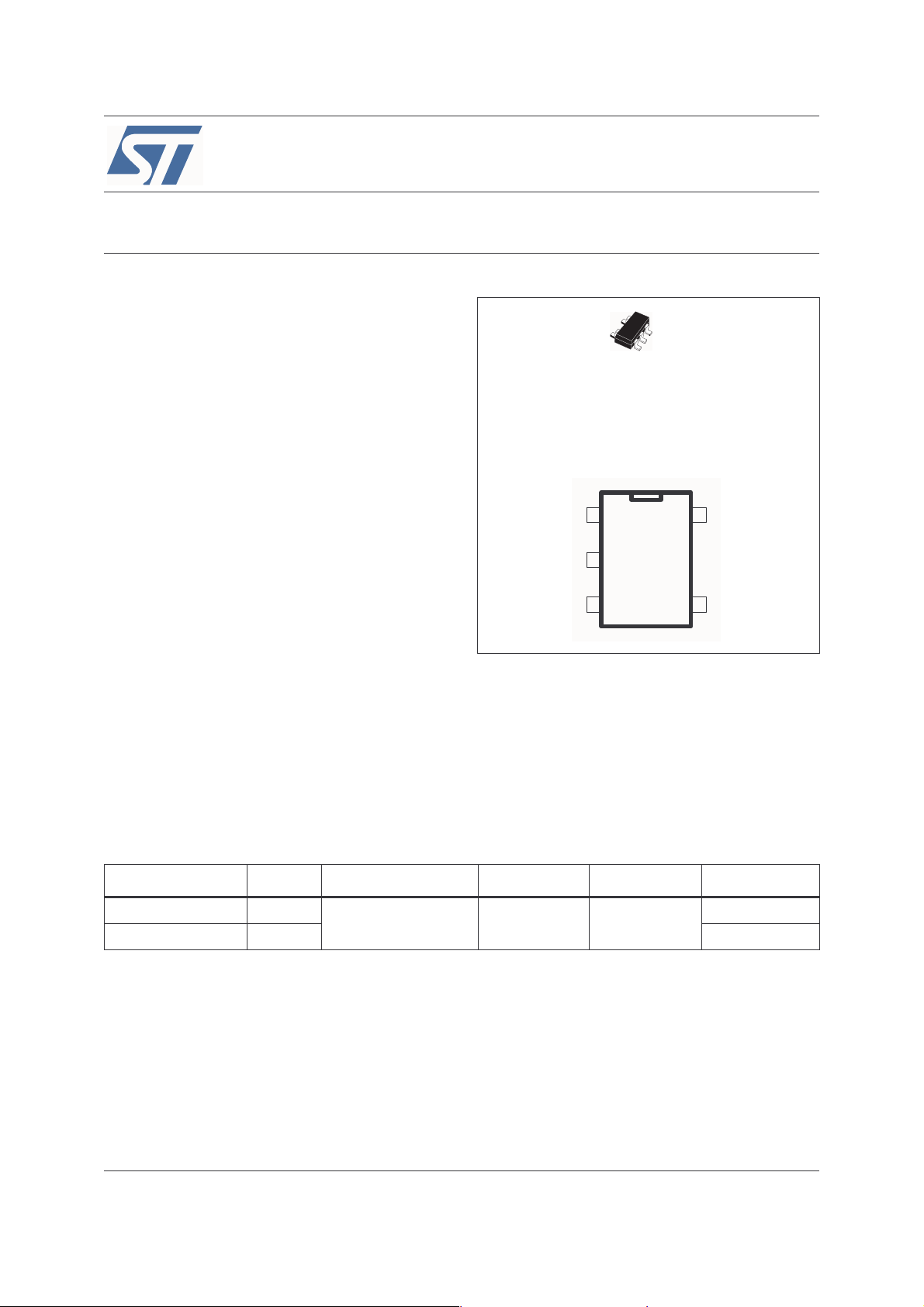
TS4431
SOT23-5L
(Plastic Micropackage)
Description
Pin connections (top view)
The TS4431 is a four-terminal device dedicated to
low voltage Switch Mode Power Supplies (SMPS).
Vc c
Sink
5
1
It integrates a 1.224V voltage reference, an
2
amplifier, and an open collector output transistor
Gnd
in a single package. The TS4431’s operating
mode is similar to the well-known standard
34
Nc Ref
voltage reference, the TL431. It maintains the
desired feedback voltage at the REF pin in a
closed loop configuration by sinking a current
proportional to the error voltage at the REF pin.
Applications
TS4431 features an open collector transistor with
an ultra-low saturation voltage, allowing it to be
used in series with the optocoupler in an SMPS
architecture to regulate low voltage SMPS.
■ Low voltage switch mode power supplies
■ Isolated DC/DC converter
■ Computers
■ Low voltage discrete regulator
Order Codes
Part Number Accuracy Temperature Range Package Packing Marking
TS4431AILT 0.5%
-40, +85°C SOT23-5 Tape & Reel
TS4431ILT 1% L275
November 2005 1/8
L288
Rev 2
www.st.com
8
Absolute Maximum Ratings TS4431
1 Absolute Maximum Ratings
Table 1. Key parameters and their absolute maximum ratings
Symbol Parameter Value Unit
I
SINK
V
V
T
SINK
P
STD
Output sink current 30 mA
Supply voltage 12 V
CC
Output voltage 12 V
Power Dissipation
D
(1)
SOT23-5
500 mW
Storage Temperature -65 to +150 °C
Human Body Model (HBM) 2 kV
ESD
Machine Model (MM) 200 V
T
LEAD
1. PD has been calculated with T
Rth
Rth
Lead Temperature (soldering, 10 seconds) 250 °C
= 25°C, T
= 250°C/W for the SOT23-5 package
JA
= 81°C/W for the SOT23-5 package
JC
AMB
Junction
=150°C and
Table 2. Operating conditions
Symbol Parameter Value Unit
T
OPER
V
I
SINK
Operating temperature range -40 to +85 °C
Supply voltage 1.5 to 10 V
CC
Output sink current 20 mA
2/8
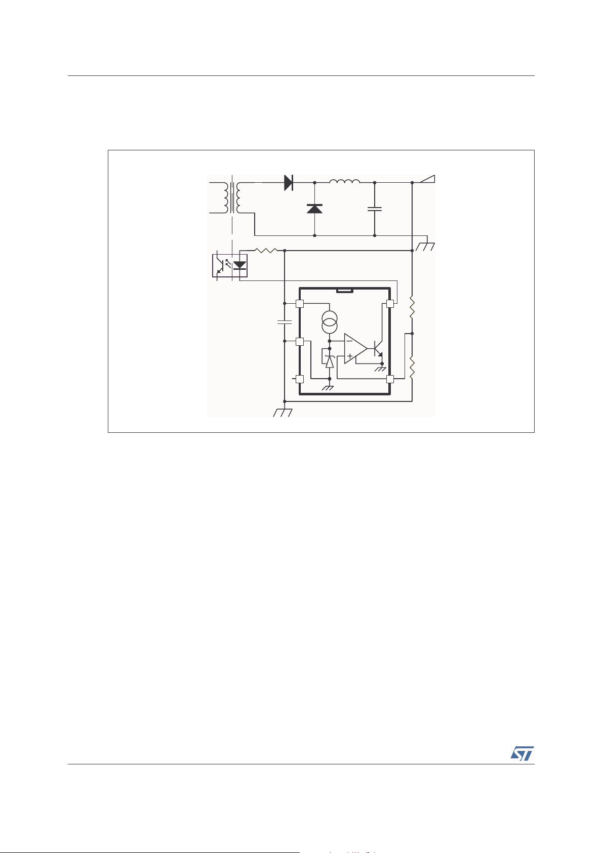
Typical Application Schematic TS4431
2 Typical Application Schematic
Figure 1. SMPS power supply: secondary side
R1
Cd1
100nF
Vout
R2
R3
Vre f
D2
L1
U1
TS4431
C1
Si nk
5
Ref
D1
Vcc
1
Gn d
2
34
Nc
3/8

Electrical Characteristics TS4431
∆
3 Electrical Characteristics
Table 3. Electrical characteristics for T
= 25°C, V
amb
= 1.8V, I
CC
= 2mA unless
SINK
otherwise specified
Symbol Parameter Test Condition Min. Typ. Max. Unit
V
REF
V
REF
T
C
∆V
REF
-----------------
∆V
CC
V
REF
-----------------
∆I
SINK
I
CC
I
OFF
I
REF
Reference voltage TS4431A 0.5%
-40°C < T < +85°C 1.209 1.239
Reference voltage TS4431 1%
-40°C < T < +85°C 1.203 1.245
Temperature coefficient 100 ppm/°C
Change in V
V
CC
Change in V
I
SINK
REF
REF
Supply current
due to change in
due to change in
VCC=1.5 to 10V
-40°C < T < +85°C 2 3
I
=0.5 to 20mA
SINK
-40°C < T < +85°C 15
I
=2mA
SINK
-40°C < T < +85°C 350
Ref < 0.6V 15 20
OFF-State supply current
-40°C < T < +85°C 30
SINK
< 10mA
Reference input current
0.1< I
-40°C < T < +85°C 2
1.218 1.224 1.230
1.212 1.224 1.236
12
710
250 300
0.4 1
V
V
mV
mV
µA
µA
µA
I
=5mA
SINK
V
Output transistor saturation
SAT
voltage
-40°C < T < +85°C 60
I
=20mA
SINK
30 50
mV
90 100
-40°C < T < +85°C 120
I
Output leakage current
OH
V
SINK=VCC
-40°C < T < +85°C 0.1
0.05
µA
Note: Limits are 100% production tested at 25°C. Limits over temperature are guaranteed through
correlation and by design.
4/8

Electrical Characteristics TS4431
Figure 2. Vref vs. temp. Isink=2mA Figure 3. Vref vs. temp. Isink=2mA
Vref (V)
1.225
1.224
1.223
1.222
1.221
1.22
1.219
1.218
-40°C -20°C 0°C 25°C 50°C 85°C
Temperature (°C)
Vcc=1.8V
Vref ( V)
1.228
1.226
1.224
1.222
1.22
1.218
1.216
-40°C -20°C 0°C 25°C 50°C 85°C
Temperature (°C)
Vcc=10V Vcc=1.5V
Figure 4. dVref/dVcc vs. temp. Isink=2mA Figure 5. Icc vs. temp. Isink=2mA
1.6
1.4
1.2
1
0.8
0.6
0.4
dVref/dVcc (mV)
0.2
0
-40°C -20°C 0°C 25°C 50°C 85°C
Tem perature (°C)
350
300
250
200
150
Icc (µA)
100
50
0
-40°C -20°C 0°C 25°C 50°C 85°C
Temperature (°C)
Vcc=1.5V to 10V
Vcc=1.8V
Figure 6. Icc vs. temp. Isink=2mA Figure 7. Vref vs. temp. Vcc=1.8V
400
350
300
250
200
150
Icc (µA)
100
50
0
-40°C -20°C 0°C 25°C 50°C 85°C
Tem perature (°C)
Vcc=1.5V Vcc=10V
1.235
1.23
1.225
Vref (V)
1.22
1.215
-40°C -20°C 0°C 25°C 50°C 85°C
Temperature (°C)
Is i nk= 2 0mA Isink=0.5mA
5/8

Electrical Characteristics TS4431
Figure 8. dVref/dIsink vs. temp. Vcc=1.8V Figure 9. Iref vs. temp. Vcc=1.8V
8
7
6
5
4
3
2
dVref/DIsink (mV)
1
0
-40°C -20°C 0°C 25°C 50°C 85°C
Tem perature (°C)
Isink 0.5 to 20mA
Figure 10. Vsat vs. temp. Vcc=1.8V
100
80
60
40
Vsat (mV)
20
0
-40°C -20°C 0°C 25°C 50°C 85°C
Tem perature (°C)
0.8
0.7
0.6
0.5
0.4
0.3
Iref (µA)
0.2
0.1
0
-40°C -20°C 0°C 25°C 50°C 85°C
Tem per ature (°C)
Isink 0.1 to 10mA
Is ink =20 mA Is i nk = 5mA
6/8

TS4431 Package Mechanical Data
4 Package Mechanical Data
In order to meet environmental requirements, ST offers these devices in ECOPACK® packages.
These packages have a Lead-free second level interconnect. The category of second level
interconnect is marked on the package and on the inner box label, in compliance with JEDEC
Standard JESD97. The maximum ratings related to soldering conditions are also marked on
the inner box label. ECOPACK is an ST trademark. ECOPACK specifications are available at:
www.st.com
SOT23-5L Package
.
SOT23-5L MECHANICAL DATA
DIM.
A 0.90 1.45 35.4 57.1
A1 0.00 0.15 0.0 5.9
A2 0.90 1.30 35.4 51.2
b 0.35 0.50 13.7 19.7
C 0.09 0.20 3.5 7.8
D 2.80 3.00 110.2 118.1
E 2.60 3.00 102.3 118.1
E1 1.50 1.75 59.0 68.8
e.95 37.4
e1 1.9 74.8
L 0.35 0.55 13.7 21.6
MIN. TYP MAX. MIN. TYP. MAX.
mm. mils
0
7/8

Revision History TS4431
5 Revision History
Date Revision Changes
March 2005 1 First release corresponding to Preliminary Data version of datasheet.
Nov. 2005 2 First release of fully mature product data sheet.
Information furnished is believed to be accurate and reliable. However, STMicroelectronics assumes no responsibility for the consequences
of use of such information nor for any infringement of patents or other rights of third parties which may result from its use. No license is
granted by implication or otherwise under any patent or patent rights of STMicroelectronics. Specifications mentioned in this publication are
subject to change without notice. This publication supersedes and replaces all information previously supplied. STMicroelectronics products
are not authorized for use as critical components in life support devices or systems without express written approval of STMicroelectronics.
The ST logo is a registered trademark of STMicroelectronics.
All other names are the property of their respective owners
© 2005 STMicroelectronics - All rights reserved
STMicroelectronics group of companies
Australia - Belgium - Brazil - Canada - China - Czech Republic - Finland - France - Germany - Hong Kong - India - Israel - Italy - Japan -
Malaysia - Malta - Morocco - Singapore - Spain - Sweden - Switzerland - United Kingdom - United States of America
www.st.com
8/8
 Loading...