ST TS419, TS421 User Manual

TS419
TS421
360mW MONO AMPLIFIER WITH STANDBY MODE
■OPERATING FROM Vcc=2V to 5.5V
■STANDBY MODE A CTIV E HIGH (TS419) or
LOW (TS421)
■OUTPUT POWER into 16Ω: 367mW @ 5V
with 10% THD+N max or 295mW @5V and
110mW @3.3V with 1% THD+N max.
■LOW CURRENT CONSUMPTION: 2.5mA max
■High Signal-to-Noise ratio: 95dB(A) at 5V
■PSRR: 56dB typ. at 1kHz, 46dB at 217Hz
■SHORT CIRCUIT LIMITATION
■ON/OFF click reduction circuitry
■Available in SO8, MiniSO8 & DFN 3x3
DESCRIPTION
The TS419/TS421 is a monaural audio power amplifier driving in BTL mode a 16 or 32Ω earpiece or
receiver speaker. The main advantage of this configuration is to get rid of bulky ouput capacitors.
Capable of descending to lo w voltages , it delivers
up to 220mW per channel (into 16Ω loads) of continuous average power with 0.2% THD+N in the
audio bandwidth from a 5V power supply.
An externally controlled standby mode reduces
the supply current to 10nA (typ.). The TS419/
TS421 can be configu red by external gain-setting
resistors or used in a fixed gain version.
APPLICATIONS
■16/32 ohms earpiece or receiver speaker driver
■Mobile and cordless phones (analog / digital)
■PDAs & c o mpute r s
■Portable appliances
PIN CONNECTIONS (top view)
TS419IDT: SO8
TS419IST, TS419-xIST: MiniSO8
Standby
Bypass
V+
1
2
3
IN
4
V
IN-
TS419IQT, TS419-xIQT: DFN8
1
1
GND
GND
VOUT 2
VOUT 2
2
2
3
STANDBY
STANDBY
3
BYPASS V
BYPASS V
4
4
TS421IDT: SO8
TS421IST, TS421-xIST: MiniSO8
8
7
6
5
8
8
7
7
6
6
5
5
V2
OUT
GND
CC
V
V
OUT1
Vcc
Vcc
OUT 1
OUT 1
V
V
VIN-
VIN-
IN+
IN+
ORDER CODE
Part
Number
Temp.
Range:
I
TS419
TS421
TS419
TS419-2 tba tba x2/6dB K19B
TS419-4 tba tba x4/12dB K19C
TS419-8 tba tba x8/18dB K19D
-40, +85°C
TS421
TS421-2 tba tba x2/6dB K21B
TS421-4 tba tba x4/12dB K21C
TS421-8 tba tba x8/18dB K21D
MiniSO & DFN only available in Tape & Reel with T suffix.
SO is available in Tube (D) and in Tape & Reel (DT)
June 2003
Package
DS Q
•
•
••
••
Gain Marking
external TS419I
external TS421I
external K19A
external K21A
TS421IQT, TS421-xIQT: DFN8
1
1
GND
GND
VOUT 2
VOUT 2
2
2
3
STANDBY
STANDBY
3
BYPASS V
BYPASS V
4
4
8
8
Vcc
Vcc
7
7
V
V
OUT 1
OUT 1
VIN-
VIN-
6
6
IN+
IN+
5
5
1/32
TS419-TS421
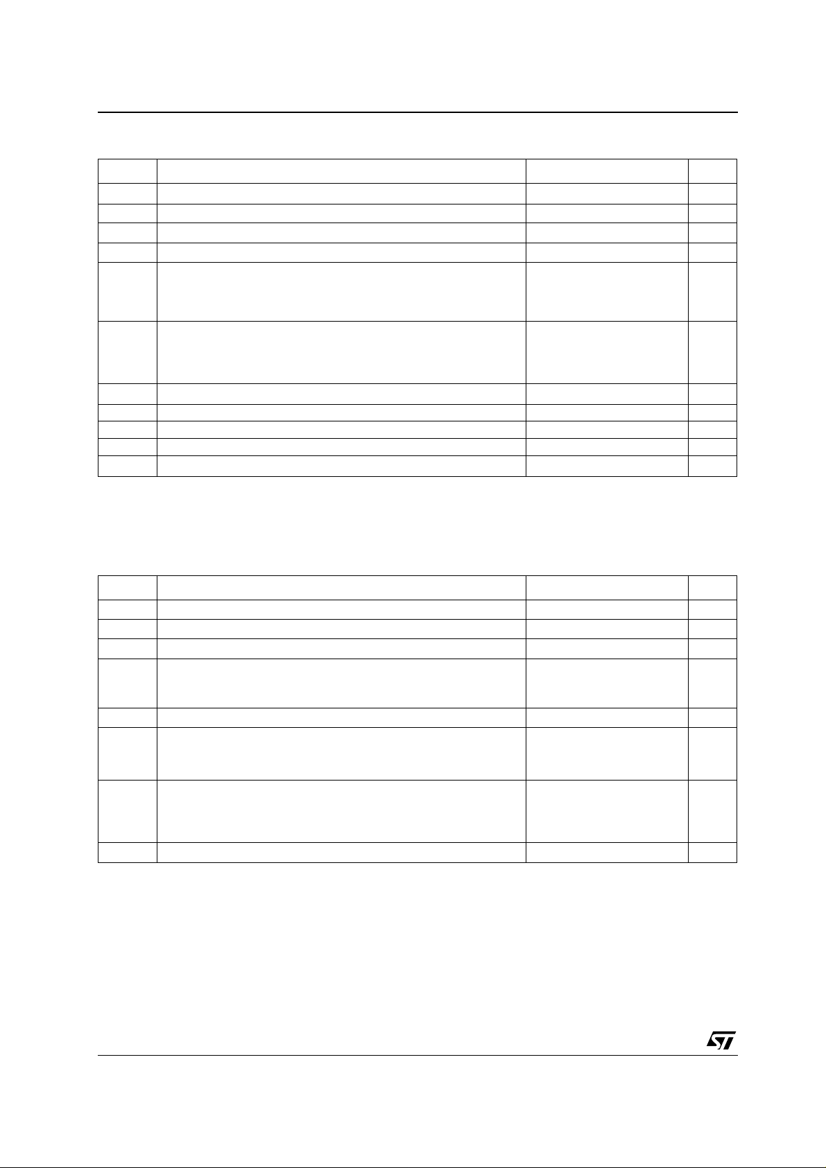
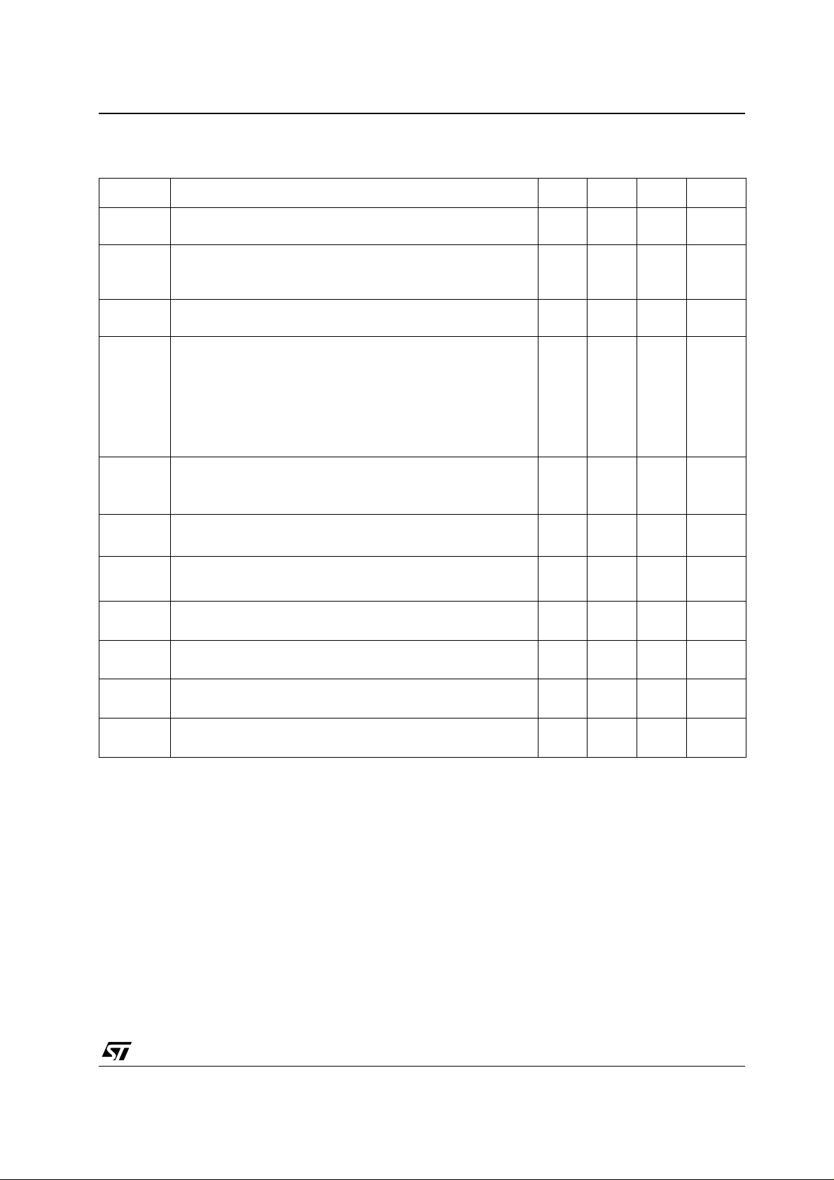
ABSOLUTE MAXIMUM RATINGS
Symbol Parameter Value Unit
V
T
R
Supply voltage
CC
V
Input Voltage
i
Storage Temperature -65 to +150 °C
stg
T
Maximum Junction Temperature 150 °C
j
Thermal Resistance Junction to Ambient
thja
SO8
MiniSO8
DFN8
Power Dissipation
Pd
SO8
MiniSO8
DFN8
ESD
Human Body Model (pin to pin): TS419
ESD Machine Model - 220pF - 240pF (pin to pin) 100 V
Latch-up Latch-up Immunity (All pins) 200 mA
Lead Temperature (soldering, 10sec ) 250 °C
Output Short-Circuit to Vcc or GND
1. All voltage values are measured with respect to the ground pin.
2. Pd has been calculated with Tamb = 25°C, Tjunction = 150°C.
3. TS419 stands 1.5KV on all pi ns except sta ndby pin which st ands 1KV.
4. Attention must be pai d to continou s power dissipat i on (V
dramatically reduci ng product lif e expectan cy .
1)
-0.3V to V
6V
+0.3V
CC
175
215
70
2)
0.71
0.58
1.79
3)
, TS421
x 300mA). Exposure of the IC to a short circuit for an extended time period is
DD
1.5 kV
continous
4)
V
°C/W
W
OPERATING CONDITIONS
Symbol Parameter Value Unit
V
T
V
V
R
T
1. The minimum current consumption (I
2. Wh en m ounted on a 4-layer PCB
3. For more details on T
Supply Voltage 2 to 5.5 V
CC
R
Load Resistor ≥ 16
L
Operating Free Air Temperature Range -40 to + 85 °C
oper
Load Capacitor
= 16 to 100
C
ICM
L
R
L
R
> 100
L
Common Mode Input Voltage Range
Standby Voltage Input
STB
TS421 ACTIVE / TS419 in STANDBY
TS421 in STANDBY / TS419 ACTIVE
Ω
Ω
GND ≤ V
400
100
GND to V
1.5 ≤ V
STB
STB
CC
≤ V
≤ 0.4
Thermal Resistance Junction to Ambient
THJA
wu Wake-up time from standby to active mode (Cb = 1µF)
SO8
MiniSO8
2)
DFN8
STANDBY
, please refer to application note section on Wak e-up time pag e 28.
WU
) is guaranteed at VCC (TS419) or GND (TS421) for the whole temperature range.
3)
150
190
41
0.12 s
≥
-1V
CC
1)
Ω
pF
V
V
°C/W
2/32
TS419-TS421
FIXED GAIN VERSION SPECIFIC ELECTRICAL CHARACTERISTI CS
V
from +5V to +2V, GND = 0V, T
CC
Symbol Parameter Min. Typ. Max. Unit
= 25°C (unless otherwise specified)
amb
R
Input Resistance 20 k
IN
Gain value for Gain TS419/TS421-2
G
Gain value for Gain TS419/TS421-4
Gain value for Gain TS419/TS421-8
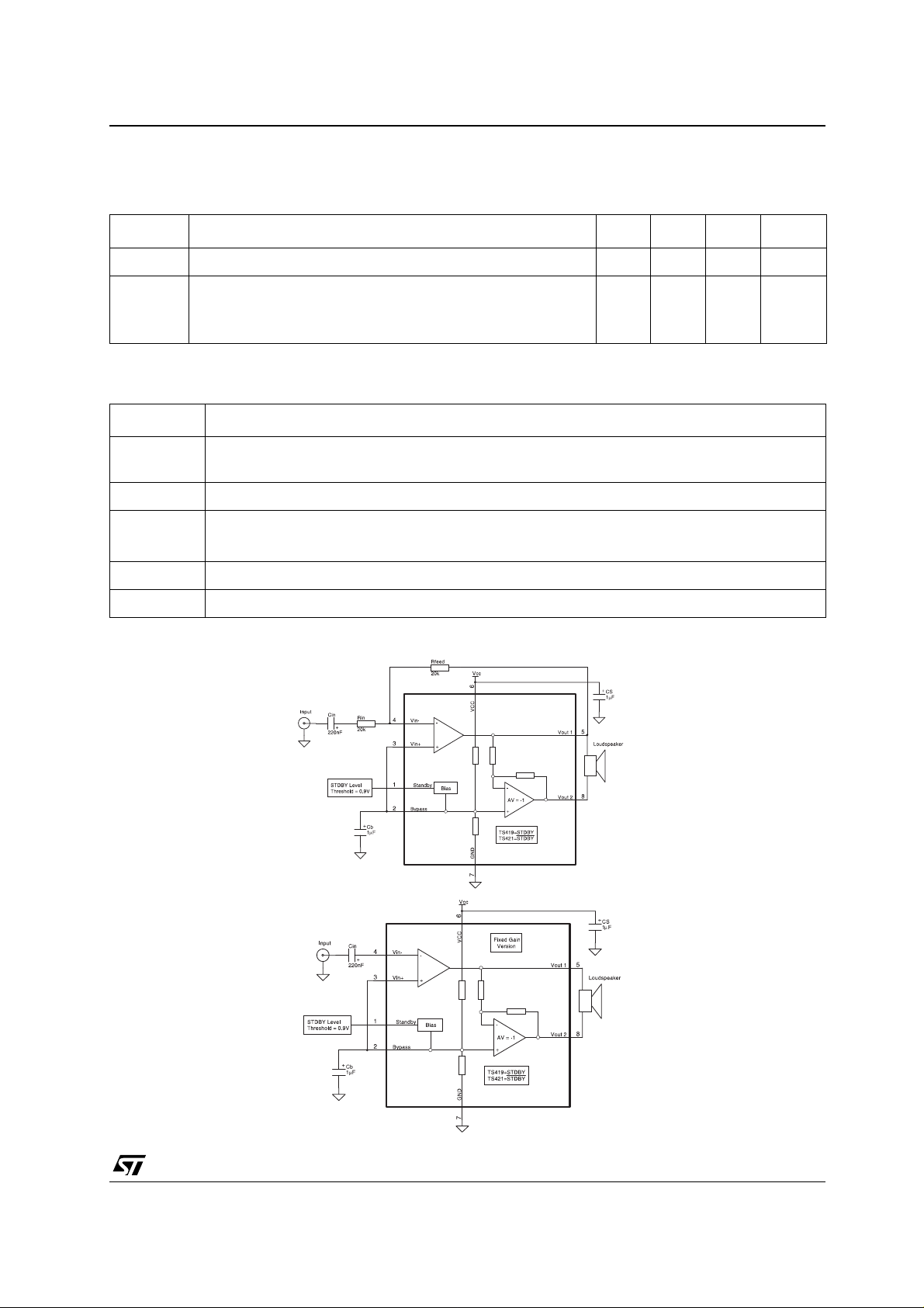
APPLICATION COMPONENTS INFORMATION
Components Functional Description
Inverting input resistor which sets the closed loop gain in conjunction with R
forms a high pass filter with C
(fcl = 1 / (2 x Pi x RIN x CIN)). Not needed in fixed gain versions.
IN
Input coupling capacitor which blocks the DC voltage at the amplifier’s input terminal
Feedback resistor which sets the closed loop gain in conjunction with RIN.
= Closed Loop Gain= 2xR
A
V
FEED/RIN
. Not needed in fixed gain versions.
Supply Bypass capacitor which provides power supply filtering.
Bypass capacitor which provides half supply filtering.
R
R
IN
C
IN
FEED
C
S
C
B
TYPICAL APPLICATION SCHEMATICS:
6dB
12dB
18dB
. This resistor also
FEED
Ω
dB
3/32
TS419-TS421
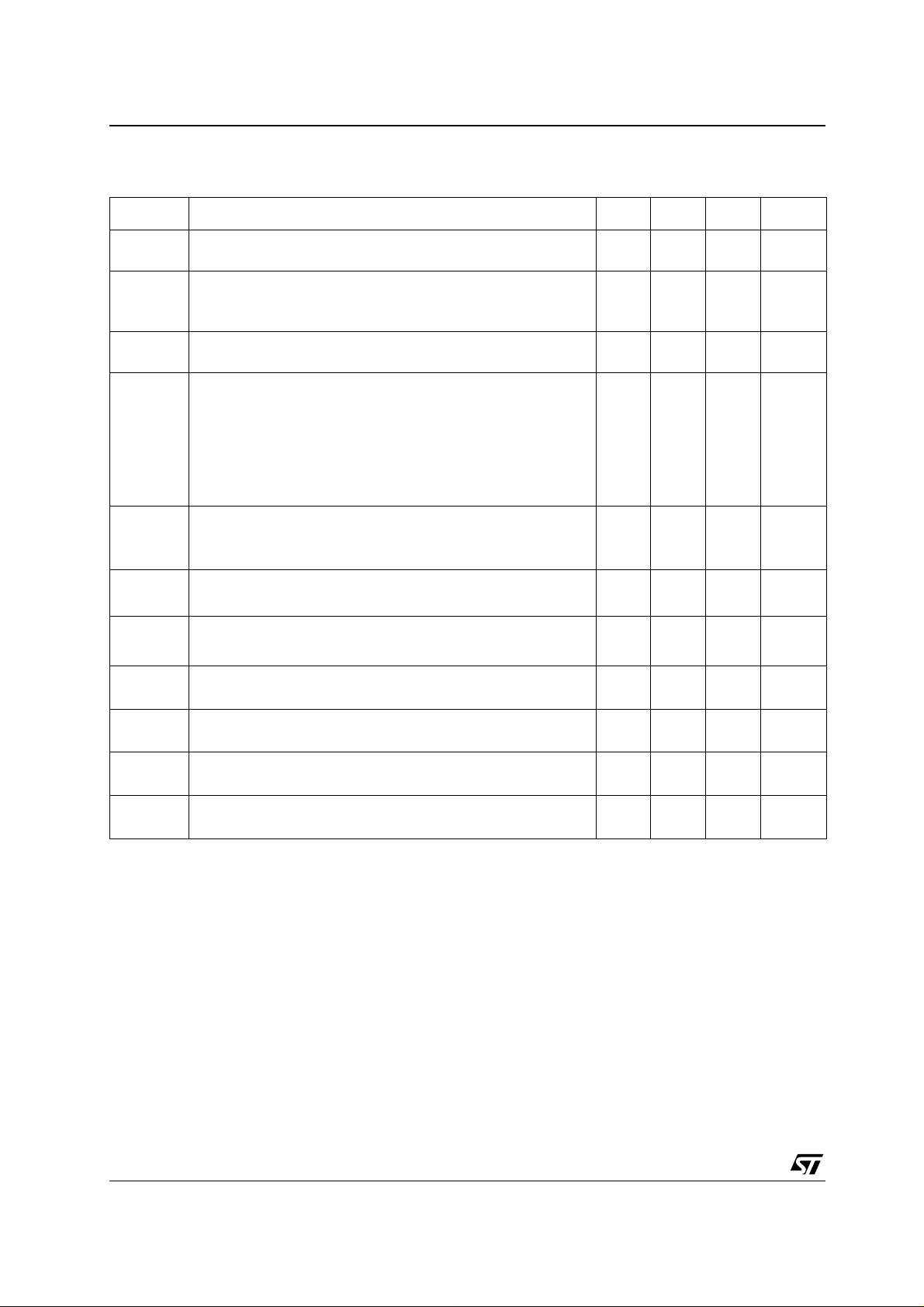
ELECTRICAL CHARACTERISTICS
= +5V, GND = 0V , T
V
CC
Symbol Parameter Min. Typ. Max. Unit
= 25°C (unless otherwise specified)
amb
I
CC
Supply Current
No input signal, no load 1.8 2.5 mA
Standby Current
I
STANDBY
No input signal, V
No input signal, V
Voo
Output Offset Voltage
No input signal, RL = 16 or 32
Output Power
THD+N = 0.1% Max, F = 1kHz, R
THD+N = 1% Max, F = 1kHz, R
P
O
THD+N = 10% Max, F = 1kHz, R
THD+N = 0.1% Max, F = 1kHz, R
THD+N = 1% Max, F = 1kHz, R
THD+N = 10% Max, F = 1kHz, R
Total Harmonic Distortion + Noise (A
R
THD + N
PSRR
SNR
Φ
GM
GBP
SR
1. Guaranteed by design and evaluation.
Power Supply Rejection Ratio (A
Signal-to-Noise Ratio (Filter Type A, A
(RL = 32
Phase Margin at Unity Gain
M
R
Gain Margin
R
Gain Bandwidth Product
R
Slew Rate
R
= 32
L
R
= 16
L
F = 1kHz, Vripple = 200mVpp, input grounded, Cb=1µF
Ω,
= 16Ω, CL = 400pF
L
= 16Ω, CL = 400pF
L
= 16
L
= 16
L
P
Ω,
out
P
Ω,
out
THD +N < 0.5%, 20Hz ≤ F ≤ 20kHz)
Ω
Ω
STANDBY
STANDBY
=GND for TS421
=Vcc for TS419
Rfeed=20k
Ω,
= 32
Ω
L
= 32
Ω
L
= 32
Ω
L
= 16
Ω
L
= 16
Ω
L
= 16
Ω
L
=2)
v
= 150mW, 20Hz ≤ F ≤ 20kHz
= 220mW, 20Hz ≤ F ≤ 20kHz
1)
=2)
v
1)
=2)
v
10 1000 nA
Ω
525mV
190
166
207
258
mW
270
240
295
367
0.15
%
0.2
50 56 dB
85 98 dB
58 Degrees
18 dB
1.1 MHz
0.4 V/µS
4/32

TS419-TS421
ELECTRICAL CHARACTERISTICS
V
= +3.3V, GND = 0V, T
CC
= 25°C (unless otherwise specified)
amb
Symbol Parameter Min. Typ. Max. Unit
1)
I
CC
Supply Current
No input signal, no load 1.8 2.5 mA
Standby Current
I
STANDBY
Voo
No input signal, V
No input signal, V
STANDBY
STANDBY
Output Offset Voltage
No input signal, RL = 16 or 32Ω, Rfeed=20k
=GND for TS421
=Vcc for TS419
Ω
Output Power
THD+N = 0.1% Max, F = 1kHz, R
THD+N = 1% Max, F = 1kHz, R
P
O
THD+N = 10% Max, F = 1kHz, R
THD+N = 0.1% Max, F = 1kHz, R
THD+N = 1% Max, F = 1kHz, R
THD+N = 10% Max, F = 1kHz, R
Total Harmonic Distortion + Noise (A
R
THD + N
PSRR
SNR
Φ
GM
GBP
SR
1. All electrical values are guaranted with correlation measurements at 2V and 5V
Power Supply Rejection Ratio
Signal-to-Noise Ratio (Weighted A, A
(R
Phase Margin at Unity Gain
M
R
Gain Margin
R
Gain Bandwidth Product
R
Slew Rate
R
= 32
L
R
= 16
L
inputs grounded, F = 1kHz, Vripple = 200mVpp, Cb=1µF
= 32
Ω,
L
= 16Ω, CL = 400pF
L
= 16Ω, CL = 400pF
L
= 16
L
= 16
L
P
= 50mW, 20Hz ≤ F ≤ 20kHz
Ω,
out
P
= 70mW, 20Hz ≤ F ≤ 20kHz
Ω,
out
THD +N < 0.5%, 20Hz ≤ F ≤ 20kHz)
Ω
Ω
=2)
v
v
=2)
= 32
L
= 32
L
= 32
L
= 16
L
= 16
L
= 16
L
Ω
Ω
Ω
Ω
Ω
Ω
10 1000 nA
525mV
75
65
81
102
mW
104
91
113
143
0.15
%
0.2
50 56 dB
82 94 dB
58 Degrees
18 dB
1.1 MHz
0.4 V/µS
5/32
TS419-TS421
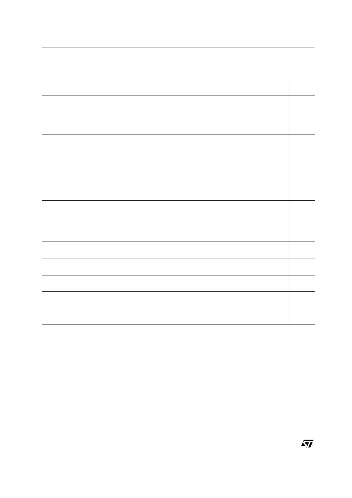
ELECTRICAL CHARACTERISTICS
V
= +2.5V, GND = 0V, T
CC
= 25°C (unless otherwise specified)
amb
1)
Symbol Parameter Min. Typ. Max. Unit
I
CC
Supply Current
No input signal, no load 1.7 2.5 mA
Standby Current
I
STANDBY
Voo
No input signal, V
No input signal, V
Output Offset Voltage
No input signal, RL = 16 or 32
STANDBY
STANDBY
=GND for TS421
=Vcc for TS419
Rfeed=20k
Ω,
10 1000 nA
Ω
525mV
Output Power
THD+N = 0.1% Max, F = 1kHz, R
THD+N = 1% Max, F = 1kHz, R
P
O
THD+N = 10% Max, F = 1kHz, R
THD+N = 0.1% Max, F = 1kHz, R
THD+N = 1% Max, F = 1kHz, R
THD+N = 10% Max, F = 1kHz, R
Total Harmonic Distortion + Noise (A
R
THD + N
PSRR
SNR
Φ
GM
GBP
SR
1. All electrical values are guaranted with correlation measurements at 2V and 5V
Power Supply Rejection Ratio (A
Signal-to-Noise Ratio (Weighted A, A
(R
Phase Margin at Unity Gain
M
R
Gain Margin
R
Gain Bandwidth Product
R
Slew Rate
R
= 32
L
R
= 16
L
inputs grounded, F = 1kHz, Vripple = 200mVpp, Cb=1µF
= 32
Ω,
L
= 16Ω, CL = 400pF
L
= 16Ω, CL = 400pF
L
= 16
L
= 16
L
P
= 30mW, 20Hz ≤ F ≤ 20kHz
Ω,
out
P
= 40mW, 20Hz ≤ F ≤ 20kHz
Ω,
out
=2)
v
THD +N < 0.5%, 20Hz ≤ F ≤ 20kHz)
Ω
Ω
=2)
v
v
=2)
= 32
L
= 32
L
= 32
L
= 16
L
= 16
L
= 16
L
Ω
Ω
32
Ω
Ω
Ω
44
Ω
37
41
52
50
55
70
0.15
0.2
50 56 dB
80 91 dB
58 Degrees
18 dB
1.1 MHz
0.4 V/µS
mW
%
6/32
TS419-TS421
ELECTRICAL CHARACTERISTICS
= +2V, GND = 0V, T
V
CC
Symbol Parameter Min. Typ. Max. Unit
= 25°C (unless otherwise specified)
amb
I
CC
Supply Current
No input signal, no load 1.7 2.5 mA
Standby Current
I
STANDBY
No input signal, V
No input signal, V
Voo
Output Offset Voltage
No input signal, RL = 16 or 32
Output Power
THD+N = 0.1% Max, F = 1kHz, R
THD+N = 1% Max, F = 1kHz, R
P
O
THD+N = 10% Max, F = 1kHz, R
THD+N = 0.1% Max, F = 1kHz, R
THD+N = 1% Max, F = 1kHz, R
THD+N = 10% Max, F = 1kHz, R
Total Harmonic Distortion + Noise (A
R
THD + N
PSRR
SNR
Φ
GM
GBP
SR
1. Guaranteed by design and evaluation.
Power Supply Rejection Ratio (A
Signal-to-Noise Ratio (Weighted A, A
(RL = 32
Phase Margin at Unity Gain
M
R
Gain Margin
R
Gain Bandwidth Product
R
Slew Rate
R
= 32
L
R
= 16
L
inputs grounded, F = 1kHz, Vripple = 200mVpp, Cb=1µF
Ω,
= 16Ω, CL = 400pF
L
= 16Ω, CL = 400pF
L
= 16
L
= 16
L
P
Ω,
out
P
Ω,
out
THD +N < 0.5%, 20Hz ≤ F ≤ 20kHz)
Ω
Ω
STANDBY
STANDBY
=GND for TS421
=Vcc for TS419
Rfeed=20k
Ω,
= 32
Ω
L
= 32
Ω
L
= 32
Ω
L
= 16
Ω
L
= 16
Ω
L
= 16
Ω
L
=2)
v
= 13mW, 20Hz ≤ F ≤ 20kHz
= 20mW, 20Hz ≤ F ≤ 20kHz
1)
=2)
v
1)
=2)
v
10 1000 nA
Ω
525mV
20
19
23
30
mW
26
24
30
40
0.1
%
0.15
49 54 dB
80 89 dB
58 Degrees
20 dB
1.1 MHz
0.4 V/µS
7/32
TS419-TS421
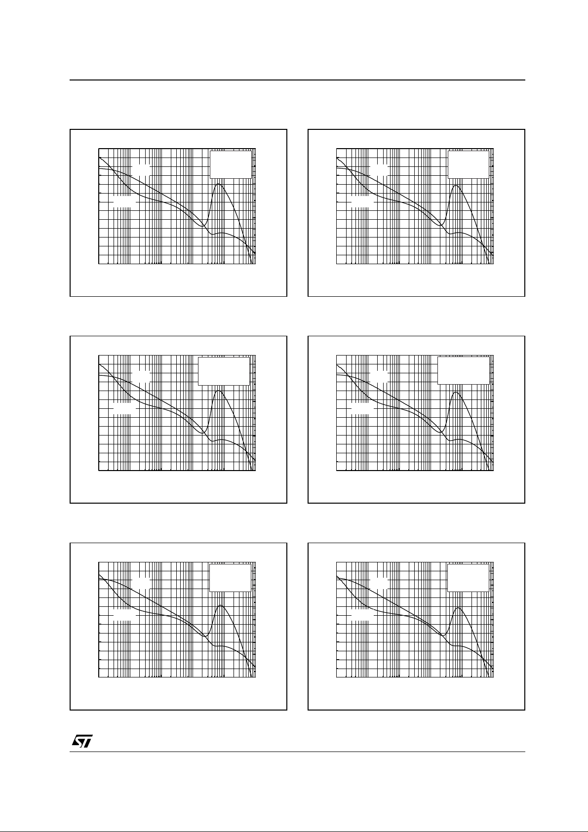
Index of Graphs
Description Figure Page
Common Curves
Open Loop Gain and Phase vs Frequency 1 to 12 9 to 10
Current Consumption vs Power Supply Voltage 13 11
Current Consumption vs Standby Voltage 14 to 19 11 to 12
Output Power vs Power Supply Voltage 20 to 23 12
Output Power vs Load Resistor 24 to 27 12 to 13
Power Dissipation vs Output Power 28 to 31 13 to 14
Power Derating vs Ambiant Temperature 32 14
Output Voltage Swing vs Supply Voltage 33 14
Low Frequency Cut Off vs Input Capacitor 34 14
Curves With 6dB Gain Setting (Av=2)
THD + N vs Output Power 35 to 43 15 to 16
THD + N vs Frequency 44 to 46 16
Signal to Noise Ratio vs Power Supply Voltage 47 to 48 17
Noise Floor 49 to 50 17
PSRR vs Frequency 51 to 55 17 to 18
Curves With 12dB Gain Setting (Av=4)
THD + N vs Output Power 56 to 64 19 to 20
THD + N vs Frequency 65 to 67 20
Signal to Noise Ratio vs Power Supply Voltage 68 to 69 21
Noise Floor 70 to 71 21
PSRR vs Frequency 72 to 76 21 to 22
Curves With 18dB Gain Setting (Av=8)
THD + N vs Output Power 77 to 85 23 to 24
THD + N vs Frequency 86 to 88 24
Signal to Noise Ratio vs Power Supply Voltage 89 to 90 25
Noise Floor 91 to 92 25
PSRR vs Frequency 93 to 97 25 to 26
Note : All measurements made with Rin=20kΩ, Cb=1µF, and Cin=10µF unless otherwise specified.
8/32
TS419-TS421
0.1 1 10 100 1000 10000
-40
-20
0
20
40
60
80
-20
0
20
40
60
80
100
120
140
160
180
Gain (dB)
Frequency (kHz)
Vcc = 2V
RL = 8
Ω
Tamb = 25°C
Gain
Phase
Phase (Deg)
0.1 1 10 100 1000 10000
-40
-20
0
20
40
60
80
-20
0
20
40
60
80
100
120
140
160
180
Gain (dB)
Frequency (kHz)
Vcc = 2V
ZL = 8Ω+400pF
Tamb = 25°C
Gain
Phase
Phase (Deg)
0.1 1 10 100 1000 10000
-40
-20
0
20
40
60
80
-20
0
20
40
60
80
100
120
140
160
180
Gain (dB)
Frequency (kHz)
Vcc = 2V
RL = 16
Ω
Tamb = 25°C
Gain
Phase
Phase (Deg)
Fig. 1: Open Loop Gain and Phase vs
Frequency
80
Phase
Gain
Frequency (kHz)
60
40
20
Gain (dB)
0
-20
-40
0.1 1 10 100 1000 10000
Vcc = 5V
RL = 8
Ω
Tamb = 25°C
Fig. 3: Open Loop Gain and Phase vs
Frequency
Vcc = 5V
ZL = 8Ω+400pF
Tamb = 25°C
80
60
40
20
Gain (dB)
0
-20
-40
0.1 1 10 100 1000 10000
Gain
Phase
Frequency (kHz)
180
160
140
120
100
80
60
40
20
0
-20
180
160
140
120
100
80
60
40
20
0
-20
Fig. 2: Open Loop Gain and Phase vs
Frequency
Phase (Deg)
Fig. 4: Open Loop Gain and Phase vs
Frequency
Phase (Deg)
Fig. 5: Open Loop Gain and Phase vs
Frequency
80
60
40
20
Gain (dB)
0
-20
-40
0.1 1 10 100 1000 10000
Gain
Phase
Frequency (kHz)
Fig. 6: Open Loop Gain and Phase vs
Frequency
Vcc = 5V
RL = 16
Tamb = 25°C
180
160
Ω
140
120
100
80
60
Phase (Deg)
40
20
0
-20
9/32

TS419-TS421
0.1 1 10 100 1000 10000
-40
-20
0
20
40
60
80
-20
0
20
40
60
80
100
120
140
160
180
Gain (dB)
Frequency (kHz)
Vcc = 2V
ZL = 16Ω+400pF
Tamb = 25°C
Gain
Phase
Phase (Deg)
0.1 1 10 100 1000 10000
-40
-20
0
20
40
60
80
-20
0
20
40
60
80
100
120
140
160
180
Gain (dB)
Frequency (kHz)
Vcc = 2V
RL = 32
Ω
Tamb = 25°C
Gain
Phase
Phase (Deg)
0.1 1 10 100 1000 10000
-40
-20
0
20
40
60
80
-20
0
20
40
60
80
100
120
140
160
180
Gain (dB)
Frequency (kHz)
Vcc = 2V
ZL = 32Ω+400pF
Tamb = 25°C
Gain
Phase
Phase (Deg)
Fig. 7: Open Loop Gain and Phase vs
Frequency
Vcc = 5V
ZL = 16Ω+400pF
Tamb = 25°C
80
60
40
20
Gain (dB)
0
-20
-40
0.1 1 10 100 1000 10000
Gain
Phase
Frequency (kHz)
Fig. 9: Open Loop Gain and Phase vs
Frequency
80
Phase
Gain
Frequency (kHz)
60
40
20
Gain (dB)
0
-20
-40
0.1 1 10 100 1000 10000
Vcc = 5V
RL = 32
Ω
Tamb = 25°C
180
160
140
120
100
80
60
40
20
0
-20
180
160
140
120
100
80
60
40
20
0
-20
Fig. 8: Open Loop Gain and Phase vs
Frequency
Phase (Deg)
Fig. 10: Open Loop Gain and Phase vs
Frequency
Phase (Deg)
Fig. 11: Open Loop Gain and Phase vs
Frequency
80
60
40
20
Gain (dB)
0
-20
-40
0.1 1 10 100 1000 10000
10/32
Gain
Phase
Frequency (kHz)
Fig. 12: Open Loop Gain and Phase vs
Frequency
Vcc = 5V
ZL = 32Ω+400pF
Tamb = 25°C
180
160
140
120
100
80
60
40
20
0
-20
Phase (Deg)
 Loading...