

1
2
3
45
6
7
8
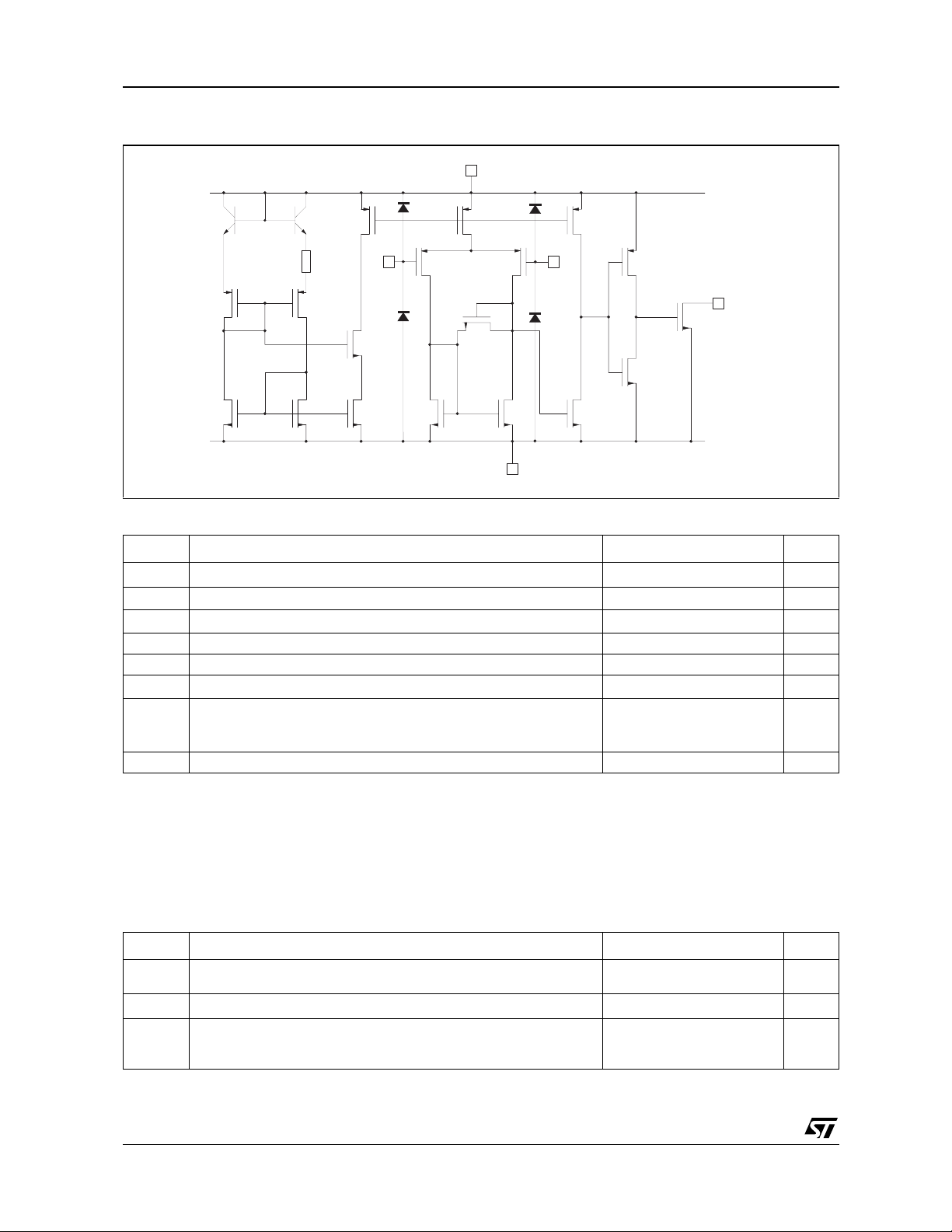
Inverting Input 2
Output 2
Non-inverting Input 2
Output 1
Inverting Input 1
Non-inverting Input 1
CC
+
V
-
CC
V
-
+
-
+
查询TS393供应商
MICROPOWER DUAL CMOS VOLTAGE COMPARATORS
TS393C,I,M
■ EXTREMELY LOW SUPPL Y CURRENT :
9µA typ / comparator
■ WIDE SINGLE SUPPLY RANGE
2.7V TO 16V OR DUAL SUPPLIES
(±1.35V TO ±8V)
■ EXTREMELY LOW INPUT BIAS CURRENT :
1pA typ
■ EXTREMELY L OW IN PUT OF F SET
CURRENTS : 1pA typ
■ INPUT COMMON-MODE VOLTAGE RANGE
INCLUDES GND
■ HIGH INPUT IMPEDANCE : 10
12
Ω typ
■ FAST RESPO NSE TIME : 2.5µs typ for
5mV overdrive
■ PIN-TO-PIN AND FUNCTIONALLY
COMPATIBLE WITH BIPOLAR LM393
DESCRIPTION
The TS393 is a micropower CMOS dual voltage
comparator with extremely low consumption of
9µA typ / comparator (20 times less than bipolar
LM393). Similar performances are offered by the
dual micropower comparator TS3702 with a
push-pull CMO S outpu t.
Thus response times remain similar to the LM393.
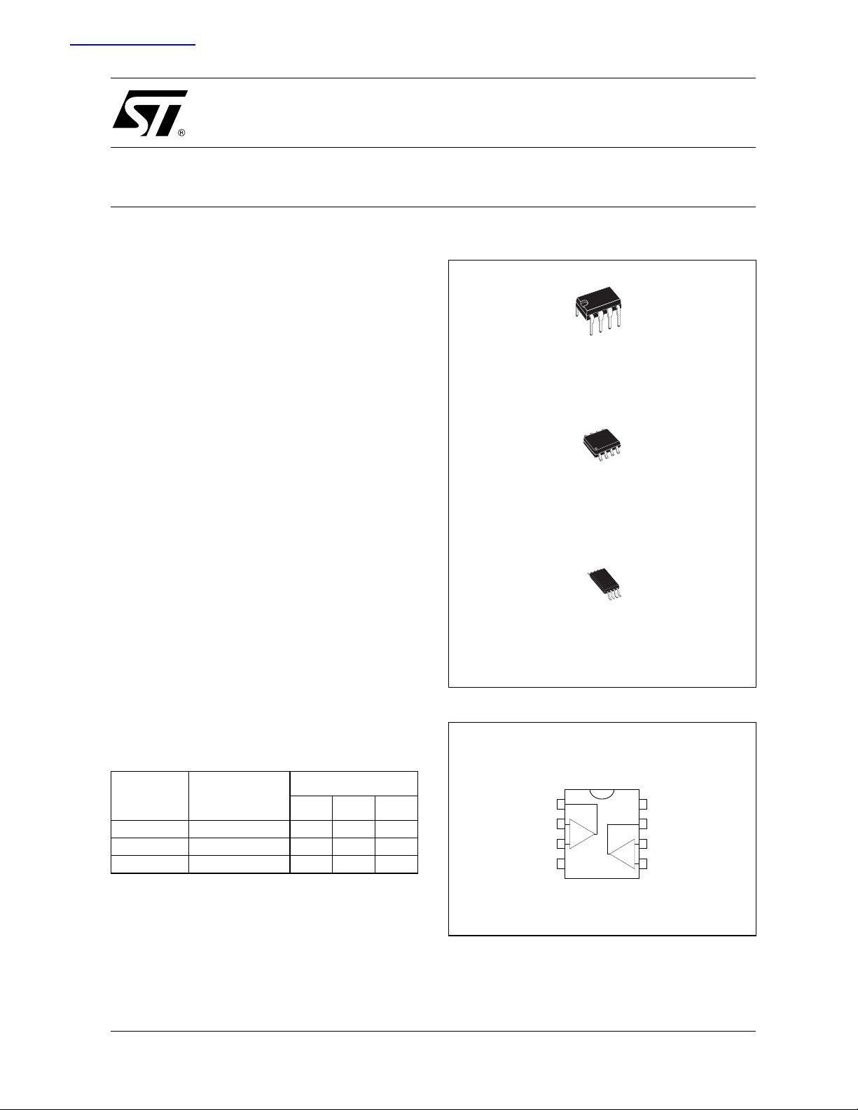
N
DIP8
(Plastic Package)
D
SO8
(Plastic Micropackage)
P
TSSOP8
(Thin Shrink Small Outline Package)
PIN CONNECTIONS (top view)
ORDER CODE
Part
Number
TS393C 0°C, +70°C
TS393I -40°C, +125°C
TS393M -55°C, +125°C
N = Dual in Line Package (DIP)
D = Small Outline Package (SO) - also available in Tape & Reel (DT)
P = Thin Shrink Small Outline Package (TSSOP) - only available
in Tape & Reel (PT)
January 2003
Temperature
Range
Package
NDP
•••
•••
•••
1/7
TS393C,I,M
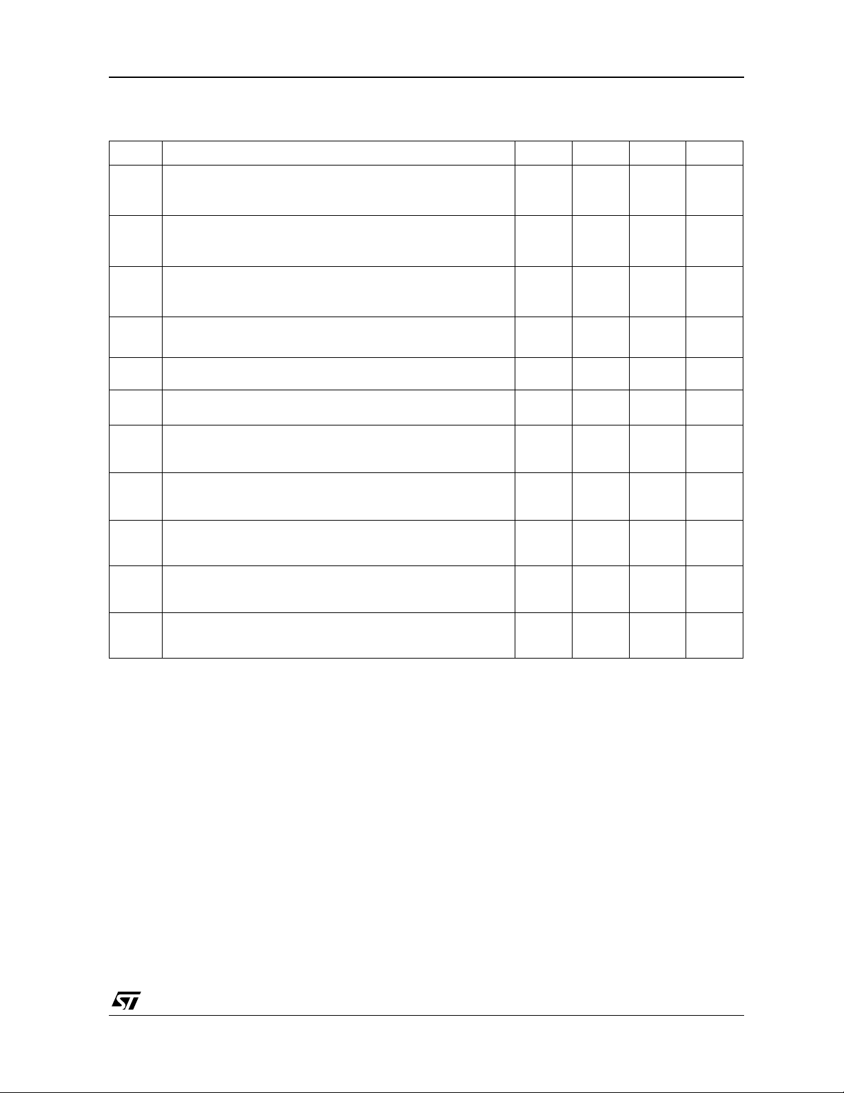
SCHEMATIC DIAGRAM (for 1/2 TS393)
T
1
T
2
T
9
V+
CC
T
10
T
17
R
1
TT
34
T
5
T
6
Input - Input +
T
8
T
7
T
11
TT
14 15
T
12
T
13
T
16
V-
CC
T
18
Output
T
20
T
19
ABSOLUTE MAXIMUM RATINGS
Symbol Parameter Value Unit
+
V
T
Supply Voltage
CC
V
Differential Input Voltage
id
V
Input Voltage
i
V
Output Voltage 18 V
o
I
Output Current 20 mA
o
I
Forward Current in ESD Protection Diodes on Inputs
F
Power Dissipation 5) DIP8
p
d
Storage Temperature Range -65 to +150 °C
stg
1. All volta ge values, except differential voltage, are w i th respect to network grou nd t erminal.
2. Differe nt i al voltages are the non-i nverting i nput termi nal with respect to the inverting input terminal .
3. Excursion s of input voltages may exceed the power supply leve l . As long as the common m ode voltage [V
within the specified range, the comparator will pr ovide a stable ou tput state. H owever, the maximum cur rent throu gh the ESD diode s (if)
of the input stage must st ri ct l y be observ ed. The output m ust never ex ceed the pow er supply voltage.
4. Guaranteed by design.
5. Pd is calculated with T
1)
2)
3)
= +25°C, Tj = +150°C and R
amb
4)
SO8
TSSOP8
= 100°C/W for DIP8 package
thja
= 175°C/W for SO8 package
= 200°C/W for TSSOP8 package
18 V
±18 V
18 V
50 mA
1250
710
625
+
in
+ V
-
)/2] remains
in
icm
=(V
mW
OPERATING CONDITIONS
Symbol Parameter Value Unit
2/7
Supply Voltage TS393C,I
+
V
CC
V
Common Mode Input Voltage Range
icm
TS393M
Operating Free-Air Temperature range TS393C
T
oper
TS393I
TS393M
2.7 to 16
4 to 16
CC
+
0 to V
0 to +70
-40 to +125
-55 to +125
-1.5
V
V
°C
TS393C,I,M
ELECTRICAL CHARACTERISTICS
+
V
= 3V, V
CC
Symbol Parameter Min. Typ. Max. Unit
V
io
I
io
I
ib
V
icm
CMR
SVR
I
OH
V
OL
I
CC
t
PLH
t
PHL
1. The specif i ed of fset voltage is the maxi m un value req ui red to drive the output up to 2.5V or down to 0.3V.
2. Maximum values incl udi ng unavoi dable inacc uracies of th e i ndustrial test.
-
= 0V, T
cc
Input Offset Voltage
= 25°C (unless otherwise specified)
amb
1)
Vic = 1.5V
. ≤ T
T
min
Input Offset Current
amb
≤ T
max.
2)
Vic = 1.5V
. ≤ T
T
min
Input Bias Current
amb
≤ T
max.
2)
Vic = 1.5V
. ≤ T
T
min
amb
≤ T
max.
Input Common Mode Voltage Range
T
. ≤ T
amb
≤ T
max
min
Common-mode Rejection Ratio
= V
V
ic
icm min.
Supply Voltage Rejection Ratio
+
V
= 3V to 5V
CC
High Level Output Current
= +1V, VOH = 3V
V
id
. ≤ T
T
min
amb
≤ T
max.
Low Level Output Voltage
V
= -1V, IOL = +6mA
id
. ≤ T
T
min
amb
≤ T
max.
Supply Current (each comparator)
No load - Outputs low
. ≤ T
T
min
amb
≤ T
max.
Response Time Low to High
V
= 0V, f = 10kHz, RL = 5.1kΩ, CL = 50pF, Overdrive = 5mV
ic
TTL Input
Response Time High to Low
= 0V, f = 10kHz, RL = 5.1kΩ, CL = 50pF, Overdrive = 5mV
V
ic
TTL Input
5
6.5
1
300
1
600
+
-1.2
0
0
V
CC
+
-1.5
V
CC
70
70
240
1000
400 550
800
920
25
1.5
0.7
2.5
0.08
mV
pA
pA
V
dB
dB
nA
mV
µ
µ
µ
A
s
s
3/7

TS393C,I,M
ELECTRICAL CHARACTERISTICS
+
V
= 5V, V
CC
Symbol Parameter Min. Typ. Max. Unit
V
io
I
io
I
ib
V
icm
CMR
SVR
I
OH
V
OL
I
CC
t
PLH
t
PHL
t
f
1. The specif i ed of fset voltage is the maxi m un value req ui red to drive the output up to 4.5V or down to 0.3V.
2. Maximum values incl udi ng unavoi dable inacc uracies of th e i ndustrial test.
-
= 0V, T
cc
= 25°C (unless otherwise specified)
amb
Input Offset Voltage
= 2.5V, V
V
ic
T
. ≤ T
min
amb
cc
≤ T
Input Offset Current
+
= 5V to 10V
max.
2)
1)
Vic = 2.5V
. ≤ T
T
min
Input Bias Current
amb
≤ T
2)
max.
Vic = 2.5V
. ≤ T
T
min
amb
≤ T
max.
Input Common Mode Voltage Range
T
. ≤ T
amb
≤ T
max
min
Common-mode Rejection Ratio
= V
V
ic
icm min.
Supply Voltage Rejection Ratio
+
V
= +5V to +10V
CC
High Level Output Current
= 1V, VOH = +5V
V
id
. ≤ T
T
min
amb
≤ T
max.
Low Level Output Voltage
V
= -1V, IOL = 6mA
id
. ≤ T
T
min
amb
≤ T
max.
Supply Current (each comparator)
No load - Outputs low
. ≤ T
T
min
amb
≤ T
max.
Response Time Low to High
V
= 0V, f = 10kHz, RL = 5.1kΩ, CL = 50pF, Overdrive = 5mV
ic
Overdrive = 10mV
Overdrive = 20mV
Overdrive = 40mV
TTL Input
Response Time High to Low
= 0V, f = 10kHz, RL = 5.1kΩ, CL = 50pF, Overdrive = 5mV
V
ic
Overdrive = 10mV
Overdrive = 20mV
Overdrive = 40mV
TTL Input
Fall time
f = 10kHz, C
= 50pF, RL = 5.1kΩ, Overdrive 50mV
L
1.4 5
mV
6.5
1
300
1
600
+
-1.2
0
0
V
CC
+
-1.5
V
CC
71
80
240
1000
260 400
mV
650
10 20
25
1.5
1.2
1.0
0.8
0.7
2.5
1.9
1.2
0.8
0.08
25
pA
pA
V
dB
dB
nA
µ
µ
µ
ns
A
s
s
4/7

PACKAGE MECHANICAL DATA
8 PINS - PLASTIC DIP
TS393C,I,M
Dimensions
Min. Typ. Max. Min. Typ. Max.
A 3.32 0.131
a1 0.51 0.020
B 1.15 1.65 0.045 0.065
b 0.356 0.55 0.014 0.022
b1 0.204 0.304 0.008 0.012
D 10.92 0.430
E 7.95 9.75 0.313 0.384
e 2.54 0.100
e3 7.62 0.300
e4 7.62 0.300
F 6.6 0260
i 5.08 0.200
L 3.18 3.81 0.125 0.150
Z 1.52 0.060
Millimeters Inches
5/7

TS393C,I,M
PACKAGE MECHANICAL DATA
8 PINS - PLASTIC MICROPACKAGE (SO)
A
a2
L
c1
C
a3
b
e3
D
8
1
M
5
4
s
F
a1
E
b1
Millimeters Inches
Dimensions
Min. Typ. Max. Min. Typ. Max.
A 1.75 0.069
a1 0.1 0.25 0.004 0.010
a2 1.65 0.065
a3 0.65 0.85 0.026 0.033
b 0.35 0.48 0.014 0.019
b1 0.19 0.25 0.007 0.010
C 0.25 0.5 0.010 0.020
c1 45° (typ.)
D 4.8 5.0 0.189 0.197
E 5.8 6.2 0.228 0.244
e 1.27 0.050
e3 3.81 0.150
F 3.8 4.0 0.150 0.157
L 0.4 1.27 0.016 0.050
M 0.6 0.024
S 8° (max.)
6/7

PACKAGE MECHANICAL DATA
8 PINS - THIN SHRINK SMALL OUTL INE PAC KAGE (TSSOP)
k
c
E1
0.25mm
.010 inch
GAGE PLANE
SEATING
PLANE
L
L
C
TS393C,I,M
L1
L1
A
A2
A1
5
D
b
PIN 1 IDENTIFICATION
5
8
8
E
4
e
1
14
Millimeters Inches
Dimensions
Min. Typ. Max. Min. Typ. Max.
A 1.20 0.05
A1 0.05 0.15 0.01 0.006
A2 0.80 1.00 1.05 0.031 0.039 0.041
b 0.19 0.30 0.007 0.15
c 0.09 0.20 0.003 0.012
D 2.90 3.00 3.10 0.114 0.118 0.122
E 6.40 0.252
E1 4.30 4.40 4.50 0.169 0.173 0.177
e 0.65 0.025
k 0° 8° 0° 8°
l 0.50 0.60 0.75 0.09 0.0236 0.030
L 0.45 0.600 0.75 0.018 0.024 0.030
L1 1.000 0.039
Inform ation f urnished is beli eved to b e accu rate an d reliab le. Howe ver, ST Micro electro nics ass umes no respo nsibility for th e
consequences of use of such information nor f or a ny infringement of patent s or other ri ghts of t hird parti es which ma y result
from its use. No license is granted by implication or otherwise under any patent or patent rights of STMicroelectronics.
Specifications mentioned in this publication are subject to change witho ut notic e. This public ation sup ersedes and rep laces all
information previously supplied. STMicroelectroni cs products are not authorized for use as critical components in life support
devices or systems without express written approval of STMicroelectronics.
© The ST logo is a registered trademark of STMicroelectronics
© 2003 STM icroelectronics - Printed in Italy - All Ri g h ts Reserv ed
STMicroelectronics GROUP OF COMPANIES
Australia - Brazi l - Canada - Ch i na - F i nl and - Franc e - Germany - Hong Kong - India - Israel - Italy - Japan - Malays i a
Malta - Mo rocco - Singapore - Spain - Sweden - S wi tzerland - United Kingdom - Unit ed States
© htt p://www.s t.co m
7/7

Copyright © Each Manufacturing Company.
All Datasheets cannot be modified without permission.
This datasheet has been download from :
www.AllDataSheet.com
100% Free DataSheet Search Site.
Free Download.
No Register.
Fast Search System.
www.AllDataSheet.com
 Loading...