

Micropower dual CMOS voltage comparators
1
2
3
45
6
7
8
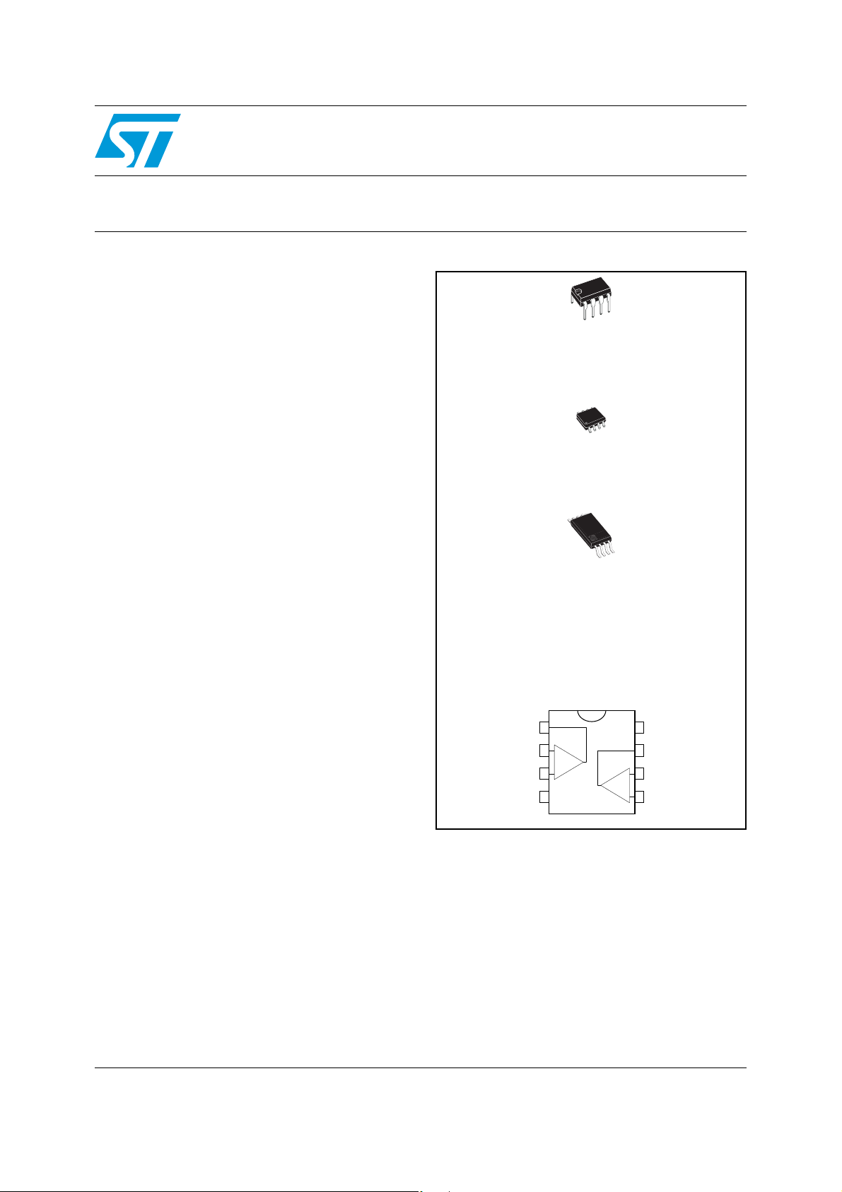
Inverting Input 2
Output 2
Non-inverting Input 2
Output 1
Inverting Input 1
Non-inverting Input 1
CC
+
V
-
CC
V
-
+
-
+
Features
■ Extremely low supply current: typically 9 µA per
comparator
■ Wide single supply range 2.7 V to 16 V or dual
supplies (±1.35 V to ±8 V)
■ Extremely low input bias current: 1 pA typical
■ Extremely low input offset current: 1 pA typical
■ Input common-mode voltage range includes
ground
■ High input impedance: 10
■ Fast response time: 2.5 µs typ. for 5 mV
overdrive
■ Pin-to-pin and functionally compatible with dual
bipolar LM393
Description
The TS393 is a micropower CMOS dual voltage
comparator with extremely low consumption of
9 µA typically per comparator (20 times less than
the dual bipolar LM393). Similar performance is
offered by the dual micropower comparator
TS3702 with a push-pull CMOS output.
12
Ω typ
TS393
N
DIP8
(Plastic package)
D
SO-8
(Plastic micropackage)
P
TSSOP8
(Thin shrink small outline package)
Pin connections
(top view)
Thus response times remain similar to the LM393.
April 2008 Rev 3 1/12
www.st.com
12
Absolute maximum ratings TS393
1 Absolute maximum ratings
Table 1. Absolute maximum ratings (AMR)
Symbol Parameter Value Unit
V
CC
V
V
V
I
I
T
R
thja
R
thjc
T
stg
ESD
+
Supply voltage
Differential input voltage
id
Input voltage
in
Output voltage 18 V
o
o
F
Output current 20 mA
Forward current in ESD protection diodes on inputs
Maximum junction temperature 150 °C
j
Thermal resistance junction to ambient
DIP8
SO-8
TSSOP8
Thermal resistance junction to case
DIP8
SO-8
TSSOP8
Storage temperature range -65 to +150 °C
HBM: human body model
MM: machine model
CDM: charged device model
(3)
(1)
(7)
(2)
(6)
(8)
(5)
(5)
(4)
18 V
±18 V
18 V
50 mA
85
125
°C/W
120
41
40
°C/W
37
500 V
200 V
1kV
1. All voltage values, except differential voltage, are with respect to network ground terminal.
2. Differential voltages are the non-inverting input terminal with respect to the inverting input terminal.
3. Excursions of input voltages may exceed the power supply level. As long as the common mode voltage
[V
However, the maximum current through the ESD diodes (IF) of the input stage must strictly be observed.
4. Guaranteed by design.
5. Short-circuits can cause excessive heating and destructive dissipation. Values are typical.
6. Human body model: A 100 pF capacitor is charged to the specified voltage, then discharged through a
1.5 kΩ resistor between two pins of the device. This is done for all couples of connected pin combinations
while the other pins are floating.
7. Machine model: A 200pF capacitor is charged to the specified voltage, then discharged directly between
two pins of the device with no external series resistor (internal resistor < 5 Ω). This is done for all couples of
connected pin combinations while the other pins are floating.
8. Charged device model: all pins and the package are charged together to the specified voltage and then
discharged directly to the ground through only one pin. This is done for all pins.
icm
=(V
+
-
+ V
in
)/2] remains within the specified range, the comparator will provide a stable output state.
in
2/12

TS393 Absolute maximum ratings
Table 2. Operating conditions
Symbol Parameter Value Unit
Supply voltage
+
V
T
V
CC
icm
oper
TS393C, TS393I 2.7 to 16
Common mode input voltage range
T
≤ T
amb
≤ T
max
min
0 to V
0 to V
Operating free-air temperature range
TS393C
TS393I
0 to +70
-40 to +125
CC
CC
+
-1.5
+
- 2
V
V
°C
3/12
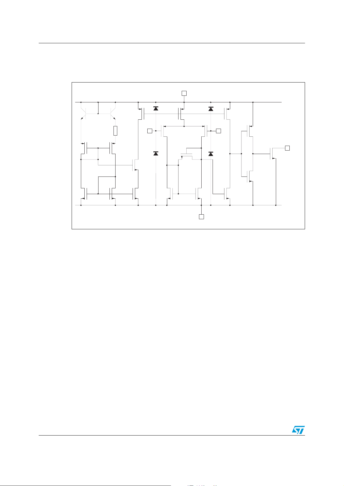
Schematic diagram TS393
2 Schematic diagram
Figure 1. Schematic diagram (for 1/2 TS393)
V+
CC
T
T
1
T
2
T
9
10
T
17
R
1
Input - Input +
TT
34
T
8
T
5
T
6
T
7
T
11
TT
14 15
T
12
T
13
T
16
V-
CC
T
18
Output
T
20
T
19
4/12
TS393 Electrical characteristics
3 Electrical characteristics
Table 3. V
CC
+
= 3V, V
Symbol Parameter Min. Typ. Max. Unit
Input offset voltage
V
io
Vic = 1.5V
T
≤ T
min
amb
Input offset current
I
io
Vic = 1.5V
≤ T
T
min
amb
Input bias current
I
ib
CMR
SVR
Vic = 1.5V
T
≤ T
min
amb
Common-mode rejection ratio
= V
V
ic
icm-min
Supply voltage rejection ratio
+
V
= 3V to 5V
CC
High level output current
I
OH
Vid = +1V, VOH = 3V
≤ T
T
min
amb
Low level output voltage
V
OL
= -1V, IOL = +6mA
V
id
T
≤ T
min
amb
Supply current (each comparator)
I
CC
No load - outputs low
≤ T
T
min
amb
Response time low to high
= 0V, f = 10kHz, RL = 5.1kΩ, CL = 50pF
V
t
PLH
ic
Overdrive = 5mV
TTL input
≤ T
≤ T
≤ T
≤ T
≤ T
≤ T
CC
(1)
max
(2)
max
2)
max
max
max
max
-
= 0V, T
= 25°C (unless otherwise specified)
amb
5
6.5
1
300
1
600
70 dB
70 dB
240
1000
400 550
800
920
25
1.5
0.7
mV
pA
pA
nA
mV
µA
µs
Response time high to low
t
PHL
1. The specified offset voltage is the maximum value required to drive the output up to 2.5 V or down to 0.3 V.
2. Maximum values include unavoidable inaccuracies of the industrial tests.
Vic = 0V, f = 10kHz, RL = 5.1kΩ, CL = 50pF
Overdrive = 5mV
TTL input
2.5
0.08
5/12
µs
Electrical characteristics TS393
Table 4. V
CC
+
= 5V, V
Symbol Parameter Min. Typ. Max. Unit
Input offset voltage
V
io
Vic = 2.5V, V
≤ T
T
min
amb
Input offset current
I
io
Vic = 2.5V
T
≤ T
min
amb
Input bias current
I
ib
CMR
SVR
Vic = 2.5V
T
≤ T
min
amb
Common-mode rejection ratio
= 0V
V
ic
Supply voltage rejection ratio
+
V
= +5V to +10V
CC
High level output voltage
I
OH
= 1V, VOH = +5V
V
id
T
≤ T
min
amb
Low level output voltage
V
OL
= -1V, IOL = 6mA
V
id
T
≤ T
min
amb
Supply current (each comparator)
I
CC
No load - outputs low
≤ T
T
min
amb
Response time low to high
= 0V, f = 10kHz, RL = 5.1kΩ, CL = 50pF,
V
ic
Overdrive = 5mV
t
PLH
Overdrive = 10mV
Overdrive = 20mV
Overdrive = 40mV
TTL input
Response time high to low
= 0V, f = 10kHz, RL = 5.1kΩ, CL = 50pF,
V
ic
Overdrive = 5mV
t
PHL
Overdrive = 10mV
Overdrive = 20mV
Overdrive = 40mV
TTL input
Fall time
t
f
f = 10kHz, C
1. The specified offset voltage is the maximum value required to drive the output up to 4.5V or down to 0.3V.
2. Maximum values including unavoidable inaccuracies of the industrial tests.
L
-
CC
(1)
+
= 5V to 10V
CC
≤ T
max
(2)
≤ T
max
2)
≤ T
max
≤ T
max
≤ T
max
≤ T
max
= 0V, T
= 25°C (unless otherwise specified)
amb
= 50pF, RL = 5.1kΩ, overdrive 50mV
1.4 5
6.5
1
300
1
600
71 dB
80 dB
240
1000
260 400
650
10 20
25
1.5
1.2
1.0
0.8
0.7
2.5
1.9
1.2
0.8
0.08
25 ns
mV
pA
pA
nA
mV
µA
µs
µs
6/12

TS393 Package information
4 Package information
In order to meet environmental requ irements, ST offers these devices in ECOPACK®
packages. These packages have a lead-free second level interconnect. The category of
second level interconnect is marked on the package and on the inner box label, in
compliance with JEDEC Standard JESD97. The maximum ratings related t o soldering
conditions are also marked on the inner box label. ECOPACK is an ST trademark.
ECOPACK specifications are available at: www.st.com
.
7/12

Package information TS393
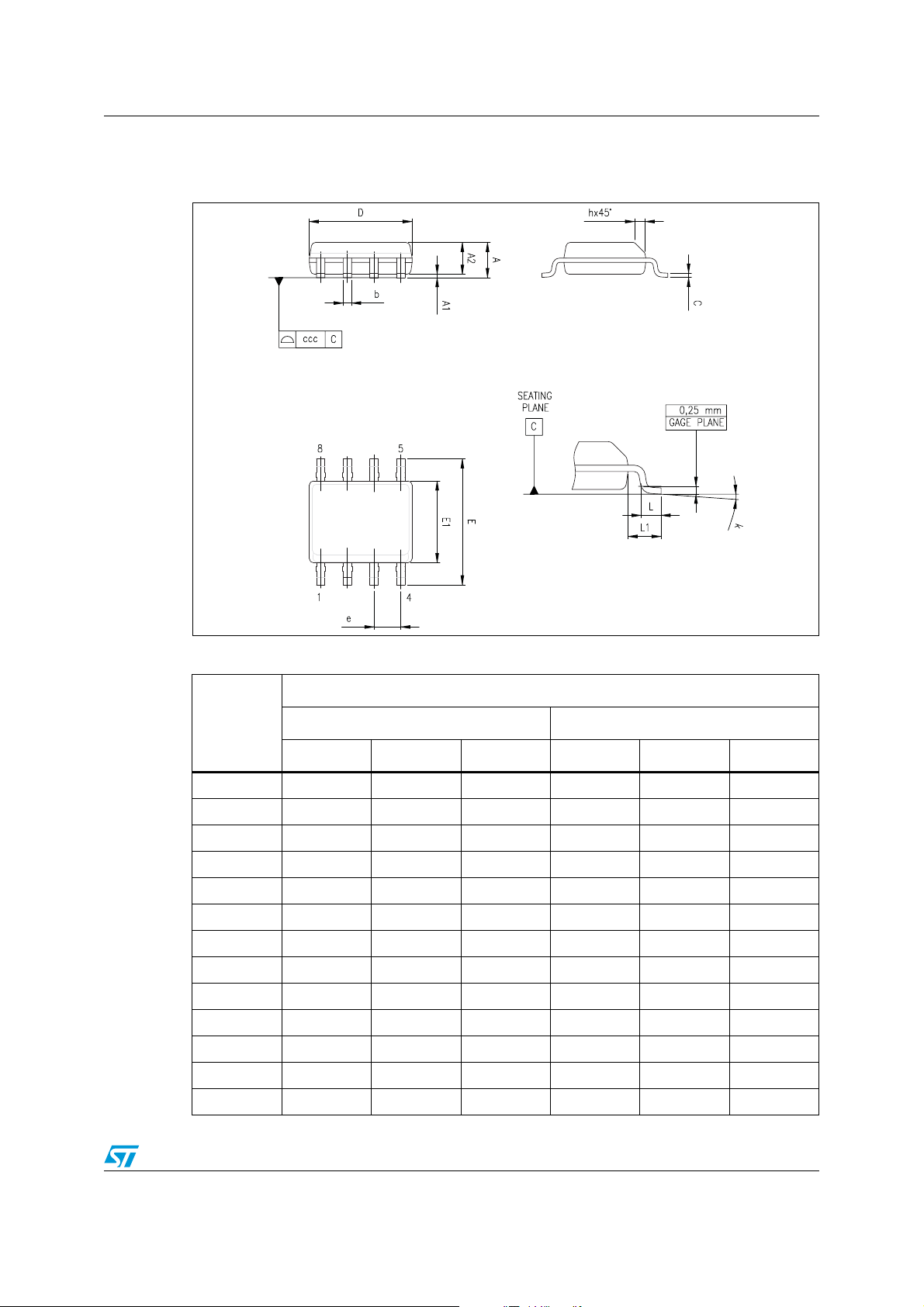
4.1 DIP8 package information
Figure 2. DIP8 package mechanical drawing
Table 5. DIP8 package mechanical data
Dimensions
Ref.
Min. Typ. Max. Min. Typ. Max.
A5.330.210
A1 0.38 0.015
A2 2.92 3.30 4.95 0.115 0.130 0.195
b 0.36 0.46 0.56 0.014 0.018 0.022
b2 1.14 1.52 1.78 0.045 0.060 0.070
c 0.20 0.25 0.36 0.008 0.010 0.014
D 9.02 9.27 10.16 0.355 0.365 0.400
E 7.62 7.87 8.26 0.300 0.310 0.325
E1 6.10 6.35 7.11 0.240 0.250 0.280
e 2.54 0.100
eA 7.62 0.300
eB 10.92 0.430
L 2.92 3.30 3.81 0.115 0.130 0.150
Millimeters Inches
8/12
TS393 Package information
4.2 SO-8 package information
Figure 3. SO-8 package mechanical drawing
Table 6. SO-8 package mechanical data
Dimensions
Ref.
Min. Typ. Max. Min. Typ. Max.
A1.750.069
A1 0.10 0.25 0.004 0.010
A2 1.25 0.049
b 0.28 0.48 0.011 0.019
c 0.17 0.23 0.007 0.010
D 4.80 4.90 5.00 0.189 0.193 0.197
E 5.80 6.00 6.20 0.228 0.236 0.244
E1 3.80 3.90 4.00 0.150 0.154 0.157
e 1.27 0.050
h 0.25 0.50 0.010 0.020
L 0.40 1.27 0.016 0.050
k1°8°1°8°
ccc 0.10 0.004
Millimeters Inches
9/12

Package information TS393
4.3 TSSOP8 package information
Figure 4. TSSOP8 package mechanical drawing
Table 7. TSSOP8 package mechanical data
Dimensions
Ref.
Min. Typ. Max. Min. Typ. Max.
A 1.2 0.047
A1 0.05 0.15 0.002 0.006
A2 0.80 1.00 1.05 0.031 0.039 0.041
b 0.19 0.30 0.007 0.012
c 0.09 0.20 0.004 0.008
D 2.90 3.00 3.10 0.114 0.118 0.122
E 6.20 6.40 6.60 0.244 0.252 0.260
E1 4.30 4.40 4.50 0.169 0.173 0.177
e 0.65 0.0256
k0°8°0°8°
L 0.45 0.60 0.75 0.018 0.024 0.030
L1 1 0.039
aaa 0.1 0.004
Millimeters Inches
10/12
TS393 Ordering information
5 Ordering information
Table 8. Order codes
Order code
Temperature
range
TS393CN
TS393CD
0°C, +70°C
TS393CDT
TS393IN
TS393ID
TS393IDT
-40°C, +125°C
TS393IPT TSSOP8 Tape & reel S393I
TS393IYD
TS393IYDT
1. Qualification and characterization according to AEC Q100 and Q003 or equivalent, advanced screening
according to AEC Q001 & Q 002 or equivalent are on-going.
(1)
(1)
-40°C, +125°C
6 Revision history
Table 9. Document revision history
Date Revision Changes
Package Packing Marking
DIP8 Tube TS393CN
SO-8
Tube or
Tape & reel
DIP8 Tube TS393IN
SO-8
SO-8
(Automotive grade)
Tube or
Tape & reel
Tube or
Tape & reel
S393C
S393I
S393IY
31-Jan-2003 1 Initial release.
31-Jul-2005 2
PPAP references inserted in the datasheet, see order codes table.
ESD protection inserted in AMR table.
Added footnotes for automotive grade order codes in order codes
28-Apr-2008 3
table.
Updated ESD values for HBM and MM.
Updated document format.
11/12

TS393
Please Read Carefully:
Information in this document is provided solely in connection with ST products. STMicroelectronics NV and its subsidiaries (“ST”) reserve the
right to make changes, corrections, modifications or improvements, to this document, and the products and services described herein at any
time, without notice.
All ST products are sold pursuant to ST’s terms and conditions of sale.
Purchasers are solely res ponsibl e fo r the c hoic e, se lecti on an d use o f the S T prod ucts and s ervi ces d escr ibed he rein , and ST as sumes no
liability whatsoever relati ng to the choice, selection or use of the ST products and services described herein.
No license, express or implied, by estoppel or otherwise, to any intellectual property rights is granted under this document. If any part of this
document refers to any third pa rty p ro duc ts or se rv ices it sh all n ot be deem ed a lice ns e gr ant by ST fo r t he use of su ch thi r d party products
or services, or any intellectua l property c ontained the rein or consi dered as a warr anty coverin g the use in any manner whats oever of suc h
third party products or servi ces or any intellectual propert y contained therein.
UNLESS OTHERWISE SET FORTH IN ST’S TERMS AND CONDITIONS OF SALE ST DISCLAIMS ANY EXPRESS OR IMPLIED
WARRANTY WITH RESPECT TO THE USE AND/OR SALE OF ST PRODUCTS INCLUDING WITHOUT LIMITATION IMPLIED
WARRANTIES OF MERCHANTABILITY, FITNESS FOR A PARTICUL AR PURPOS E (AND THEIR EQUIVALE NTS UNDER THE LAWS
OF ANY JURISDICTION), OR INFRINGEMENT OF ANY PATENT, COPYRIGHT OR OTHER INTELLECTUAL PROPERTY RIGHT.
UNLESS EXPRESSLY APPROVED IN WRITING BY AN AUTHORIZED ST REPRESENTATIVE, ST PRODUCTS ARE NOT
RECOMMENDED, AUTHORIZED OR WARRANTED FOR USE IN MILITARY, AIR CRAFT, SPACE, LIFE SAVING, OR LIFE SUSTAINING
APPLICATIONS, NOR IN PRODUCTS OR SYSTEMS WHERE FAILURE OR MALFUNCTION MAY RESULT IN PERSONAL INJ URY,
DEATH, OR SEVERE PROPERTY OR ENVIRONMENTAL DAMAGE. ST PRODUCTS WHICH ARE NOT SPECIFIED AS "AUTOMOTIVE
GRADE" MAY ONLY BE USED IN AUTOMOTIVE APPLICATIONS AT USER’S OWN RISK.
Resale of ST products with provisions different from the statements and/or technical features set forth in this document shall immediately void
any warranty granted by ST fo r the ST pro duct or serv ice describe d herein and shall not cr eate or exten d in any manne r whatsoever , any
liability of ST.
ST and the ST logo are trademarks or registered trademarks of ST in vari ous countries.
Information in this document su persedes and replaces all information previously supplied.
The ST logo is a registered trademark of STMicroelectronics. All other names are the property of their respective owners.
© 2008 STMicroelectronics - All rights reserved
STMicroelectronics group of compan ie s
Australia - Belgium - Brazil - Canada - China - Czech Republic - Finland - Fran ce - Germany - Hong Kong - India - Israel - Italy - Japan -
Malaysia - Malta - Morocco - Singapore - Spain - Sweden - Switzerland - United Kingdom - United States of America
www.st.com
12/12
 Loading...