

查询TS391供应商
LOWPOWER SINGLE VOLTAGE COMPARATORS
.WIDESINGLESUPPLYVOLTAGERANGEOR
DUAL SUPPLIES +2V TO +36V OR ±1V TO
±18V
.VERY LOW SUPPLY CURRENT (0.2mA)
INDEPENDENTOF SUPPLYVOLTAGE
(1 mW/comparatorat +5V)
.LOW INPUT BIASCURRENT : 25nATYP
.LOW INPUT OFFSET CURRENT : ±5nATYP
.LOW INPUT OFFSET VOLTAGE: ±1mV TYP
.INPUT COMMON-MODE VOLTAGE RANGE
INCLUDES GROUND
.LOW OUTPUT SATURATION VOLTAGE :
250mV TYP.(I
=4mA)
O
.DIFFERENTIAL INPUT VOLTAGE RANGE
EQUALTOTHESUPPLYVOLTAGE
.TTL, DTL, ECL, MOS, CMOS COMPATIBLE
OUTPUTS
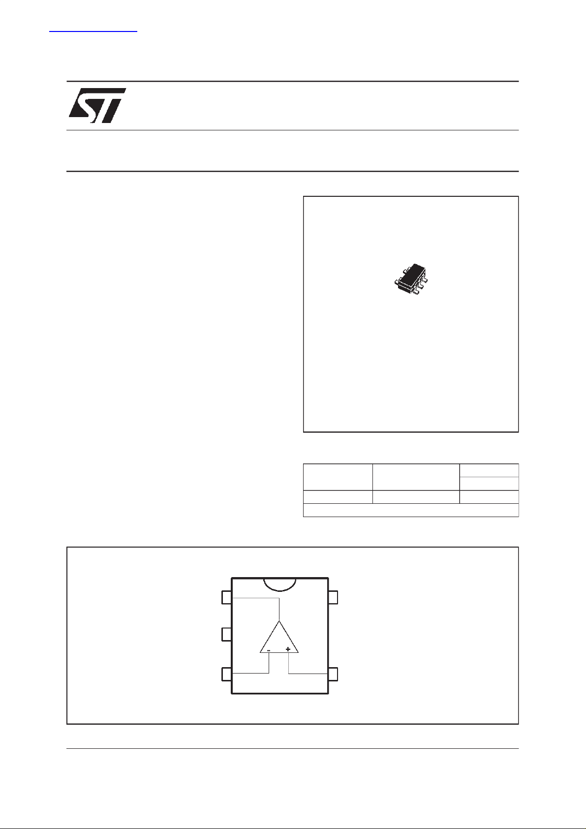
TS391
L
SOT23-5L
(Tiny Package)
DESC RIP TI ON
Thesedevicesconsistof alow power voltagecomparatordesignedspecificallyto operate froma singlesupplyoverawiderangeof voltages.Operation
fromsplitpowersuppliesis also possible.
Thiscomparatoralso hasa uniquecharacteristicin
that the input common-modevoltagerange
includesgroundeventhoughoperatedfromasingle
powersupplyvoltage.
PI N CONNECTIONS (top view)
Output
V
CC
Inverting input
1
-
2
3
ORDER CODES
Part
Number
TS391IL –40, +125
Example : TS391IL
V
5
4
Non-inverting input
CC
+
Temperature
Range
Package
o
C •
L
November 1998
1/5
TS391
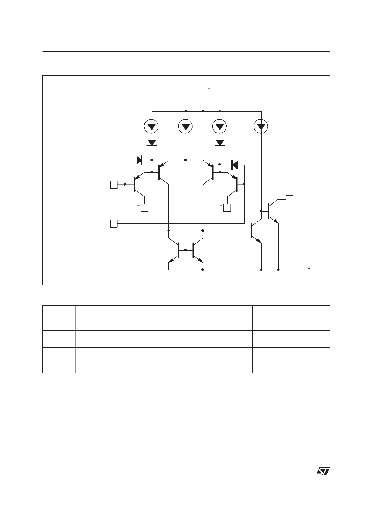
SCHE MATIC DIAGRAM
V
CC
3.5µA100
µ
A 3.5µA 100µA
Non-inverting
Input
V
V
CC
V
CC
Inverting
Input
V
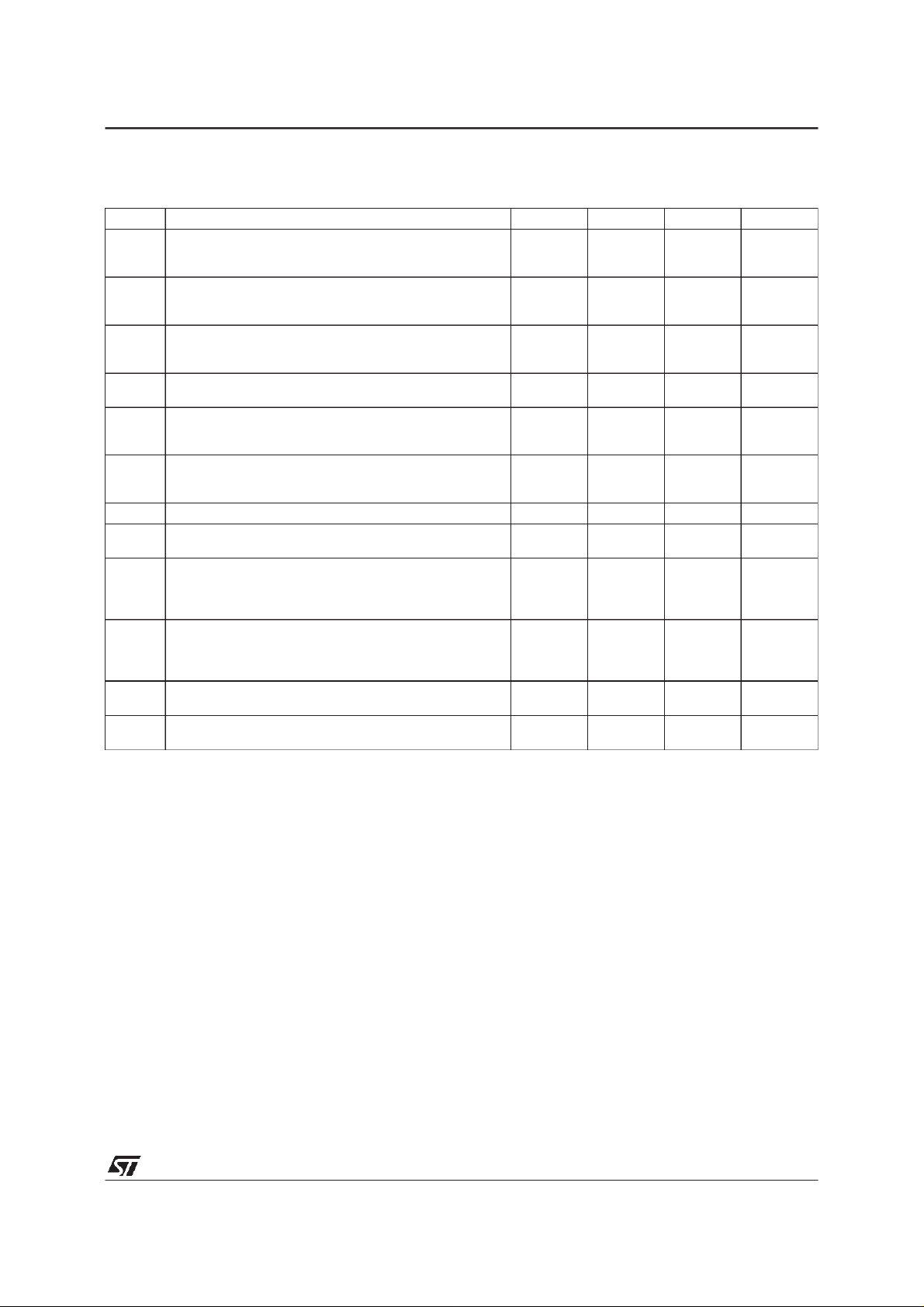
ABSOLUTE MAXIMUM RATINGS
Symbol Parameter TS391I Unit
V
CC
V
id
V
P
tot
T
oper
T
stg
Notes : 1. S hor t-cir cuit f r o m t he outp ut t o V
Supply Voltage ±18 or 36 V
Differential Input Voltage ±36 V
Input Voltage –0.3 to +36 V
i
Output Short-circuit to Ground - note 1 Infinite
Power Dissipation - note 2 500 mW
Operating Free-air TemperatureRange –40 to +125
Storage Temperature Range –65 to +150
+
can cause excessive heati ng and eventual destructi on. The maximum outpu t
current is appr oximat ely 20mA , i ndependent o f the magnitude of V
2. T
=150oC, T
j
=25oCwithR
amb
CC
=250oC/W for SOT 23- 5 package.
thja
+
.
CC
O
CC
o
C
o
C
2/5
TS391
ELECTRICAL CHARACTERISTICS
+
= +5V, V
V
CC
Symbol Parameter Min. Typ. Max. Unit
Input Offset Voltage – (note 2)
V
io
Input Bias Current – (note 3)
I
ib
Input Offset Current
I
io
A
I
V
I
V
I
Notes : 2. At ou t put switch poi nt, VO≈ 1.4V, RS=0Ωwith V
Large Signal Voltage Gain
vd
Supply Current
CC
Input Common Mode Voltage Range - (note 4)
icm
Differential Input Voltage - (note 6) V
V
id
Output Sink Current
sink
Low Level Output Voltage
OL
High Level Output Current
OH
Response Time
t
re
t
Large Signal Response Time
rel
(0V to V
3. The directi on of the inpu t current is out of t he IC due to the PNP input stage. T his current is essentially constant,
i ndepe ndent of the state of the outp ut , so no loading c h ar ge exists on the refer ence or i nput li nes.
4. The input com mon-mode volt age of either i nput si gnal v ol tage should not be allowed to go negative by m or e than
0.3V .
T he upper end of the comm on- mo de voltage ra nge is V
damage .
5. The response tim e specif ied is f or a 100 mV input st ep with 5mV overdrive. F or larger overdri ve signals 300ns can
be obtained.
6. Positi ve excursi o ns of input volt age may exceed the pow er supply level. As lon g as the other voltag e remains wi thin
the com mo n- mode range the comparator wi ll provi de a prop er out put state. The low input volt age state must not
be less t han –0. 3V ( or 0.3V below t he negati ve power supply, if u s ed) .
–
= 0V, T
CC
= +25oC
T
amb
. ≤ T
T
min
amb
= +25oC
T
amb
. ≤ T
T
min
amb
= +25oC
T
amb
. ≤ T
T
min
amb
= 15V, RL=15kΩ,Vo= 1 to 11V 50 200
V
CC
= 5V, no load
V
CC
= 30V, no load
V
CC
= +25oC
T
amb
. ≤ T
T
min
amb
= -1V, VO= 1.5V) 6 16
(V
id
= -1V, I
(V
id
T
amb
T
min
(V
id
T
amb
T
min
(R
L
=TTL,V
(V
i
sink
=25oC
. ≤ T
amb
= 1V, VCC=VO= 30V)
=25oC
. ≤ T
amb
= 5.1kΩ to V
+
1.5V) .
CC
=25oC (unless otherwise specified)
amb
≤ T
max.
≤ T
max.
≤ T
max.
≤ T
max.
= 4mA)
≤ T
max
≤ T
max
+
) – (note 5) 1.3
CC
= +1.4 V, RL= 5.1kΩ to V
ref
CC
+
CC
0
0
) 300
+
fr om 5 V to 30V and over the full inpu t comm o n- m ode range
+
–1.5V , but either or both in put s can go to +30 V wi t hout
CC
15
9
25 250
400
550
150
0.2
0.5
0.5
1.25
+
V
-1.5
CC
+
-2
V
CC
+
CC
250 400
700
0.1
1
V/mV
mV
nA
nA
mA
V
V
mA
mV
nA
µA
µs
ns
3/5
TS391
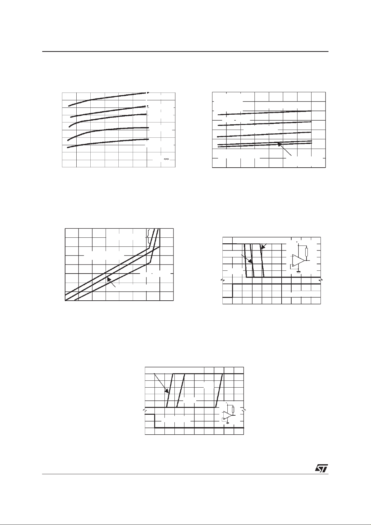
SUPPLY CURRENT versus
SUPPLY VOLTAGE
0.5
0.4
0.3
0.2
0.1
SUPPLY CURRENT (mA)
0
10 20 30 40
SUPPLY VOLTAGE (V)
OUTPUT SATURATION VOLTAGE
versus OUTPUT CURRENT
1
10
Out of saturation
0
10
T
=+125°C
amb
T
= +25°C
amb
10
-1
10
0
OUTPUT SINK CURRENT (mA)
SATURATIONVOLTAGE(V)
10
10
10
-1
-2
-3
10
-2
T
=-55 C
amb
T
amb
T=+25 C
T
amb
T
amb
T
= -55°C
amb
1
10
=0 C
=+70 C
= +125 C
R
=
10
INPUT CURRENT versus
SUP PLY VOLT AGE
80
V=0V
i
60
40
9
R=10Ω
i
T
=0°C
amb
T
amb
T
amb
= +25°C
= -55°C
20
T
= +125°C
INPUTCURRENT(nA)
amb
T
= +70°C
amb
0
10 20 30 40
SUPPLY VOLTAGE (V)
RESPONSE TIME FOR VARIOUS INPUT
OVERDRIVES - NEGATIVE TRANSITION
6
5
4
3
2
1
0
0
-50
-100
2
INPUTVOLTAGE(mV) OUTPUTVOLTAGE(V)
Input overdrive : 5mV
20mV
5V
e
I
100mV
T
= +25°C
amb
0 0.5 1 1.5 2
TIME (µs)
5.1kΩ
e
o
4/5
RESPONSE TIME FOR VARIOUS INPUT
OVERDRIVES - POSITIVE TRANSITION
6
Input overdrive : 100mV
5
INPUTVOLTAGE(mV) OUTPUTVOLTAGE(V)
100
50
4
3
2
1
20mV
0
T
= +25°C
amb
0
0 0.5 1 1.5 2
TIME (µs)
5mV
5V
5.1 k Ω
e
I
e
o
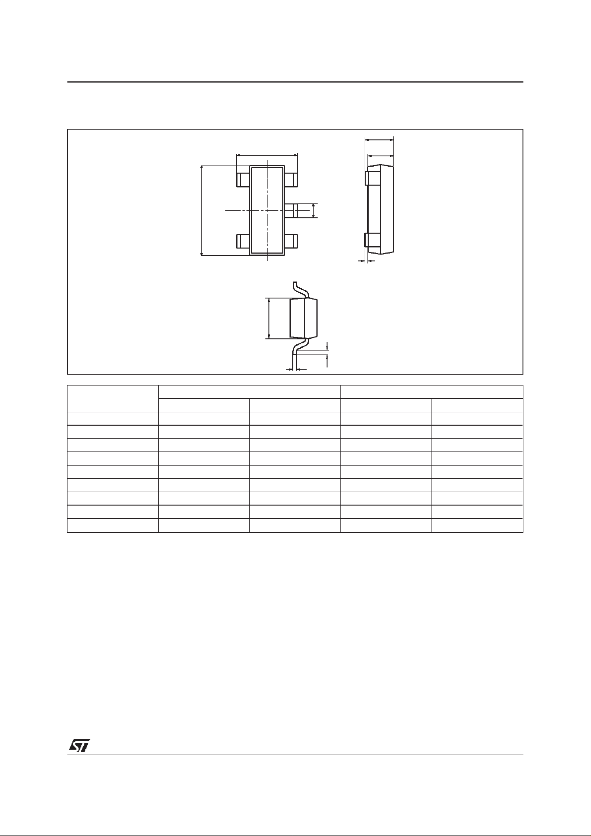
PACKAG E MECHANICAL DATA
5 PINS -TINY PACKAGE (SOT23)
TS391
A
E
A2
Dim.
D
E1
Millimeters Inches
Min. Max. Min. Max.
b
A1
L
C
A 0.90 1.45 0.034 0.057
A1 0 0.15 0.006
A2 0.90 1.30 0.034 0.051
b 0.35 0.50 0.013 0.020
C 0.09 0.20 0.003 0.008
D 2.80 3.00 0.110 0.118
E 2.60 3.00 0.102 0.118
E1 1.50 1.75 0.059 0.069
L 0.10 0.60 0.003 0.024
Information furnished is believed to be accurate and reliable. However, STMicroelectronics assumes no responsibility for the
consequences of use of such information nor for any infringement of patents or other rights of third parties which may result
from its use. No license is granted by implication or otherwise under any patent or patent rights of STMicroelectronics.
Specifications mentioned in this publication are subject to change without notice. This publication supersedes and replaces all
information previously supplied. STMicroelectronics products are not authorized for use as critical components in life support
devices or systems without express written approval of STMicroelectronics.
The ST logo is a trademark of STMicroelectronics
1998 STMicroelectronics – Printed in Italy – All Rights Reserved
STMicroelectronics GROUP OF COMPANIES
Australia - Brazil - Canada - China - France - Germany - Italy - Japan - Korea - Malaysia - Malta - Mexico - Morocco
The Netherlands - Singapore - Spain - Sweden - Switzerland - Taiwan - Thailand - United Kingdom - U.S.A.
http://www.st.com
5/5
ORDER CODE

WWW.ALLDATASHEET.COM
Copyright © Each Manufacturing Company.
All Datasheets cannot be modified without permission.
This datasheet has been download from :
www.AllDataSheet.com
100% Free DataSheet Search Site.
Free Download.
No Register.
Fast Search System.
www.AllDataSheet.com
 Loading...