

查询TS3704供应商
MICROPOWER QUAD CMOS VOLTAGE COMPARATORS
.
PUSH-PULL CMOS OUTPUT (NO EXTERNAL PULL-UPRESISTORREQUIRED)
.
EXTREMELYLOW SUPPLYCURRENT :
9µATYP / COMPARATOR
.
WIDE SINGLE SUPPLY RANGE (3V TO 16V)
OR DUAL SUPPLIES(± 1.5VTO ± 8V)
.
EXTREMELY LOW INPUT BIAS CURRENT :
1pA TYP
.
EXTREMELYLOW INPUTOFFSET
CURRENT: 1pATYP
.
INPUT COMMON-MODE VOLTAGE RANGE
INCLUDESGND
.
HIGHINPUT IMPEDANCE: 1012Ω TYP
.
FASTRESPONSE TIME : 2µs TYPFOR
5mV OVERDRIVE
.
PIN-TO-PINAND FUNCTIONALLY
COMPATIBLEWITH BIPOLAR LM339
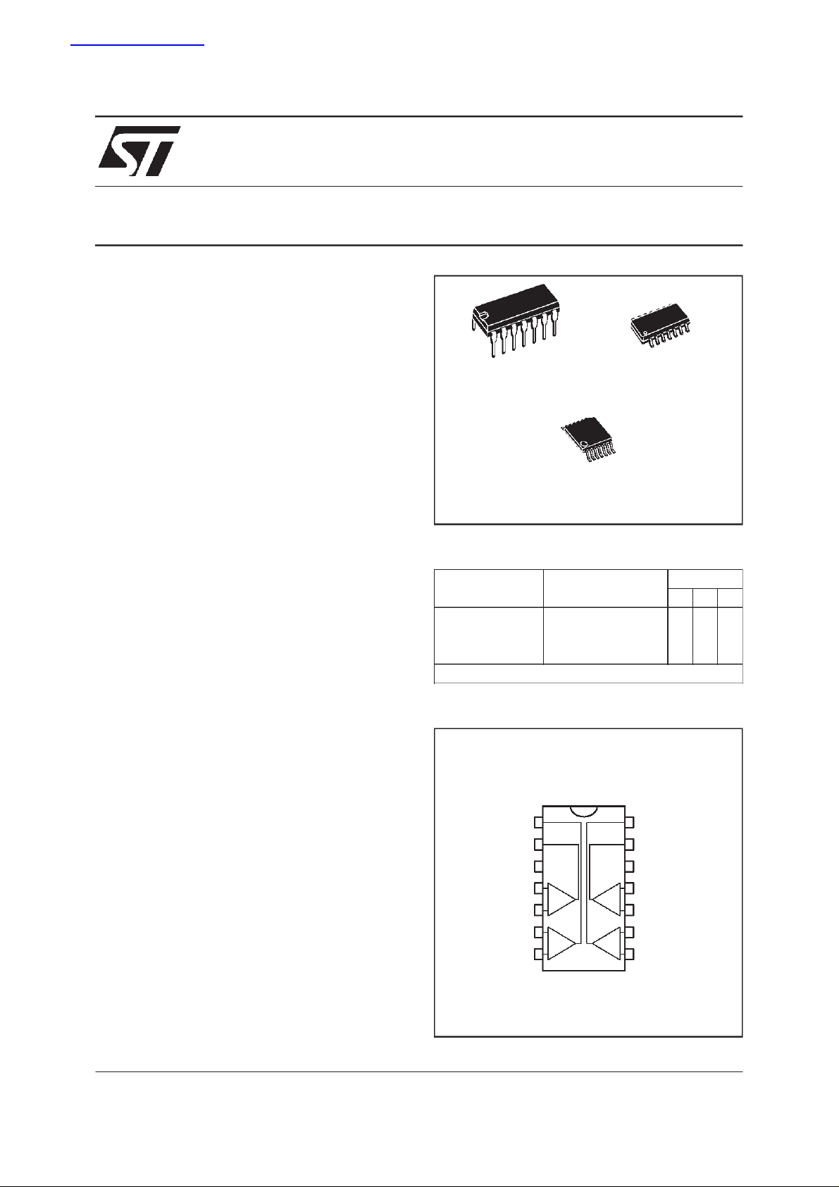
TS3704C,I,M
N
DIP14
(Plastic Package)
(Thin Shrink Small Outline Package)
ORDER CODES
Part Number Temperature Range
TS3704C 0
TS3704I -40oC, +125oC ●●●
TS3704M -55oC, +125oC ●●●
Example : TS3704CN
(Plastic Micropackage)
P
TSSOP14
o
C, +70oC ●●●
D
SO14
Package
NDP
DESCRIPTION
The TS3704is a micropower CMOS quad voltage
comparatorwith extremely low consumption
of9µAtyp / comparator(20 timesless thanbipolar
LM339). The push-pull CMOSoutputstage allows
powerandspacesavingbyeliminatingtheexternal
pull-up resistor required by usual open-collector
output comparators.
Thus responsetimes remain similarto theLM339.
January 1999
PIN CONNECTIONS (top view)
Output 2
1
Output 1
2
V
3
CC
Inverting Input 1
Non-invertingInput 1
Inverting Input 2
Non-inverting Input 2
4
-
+-
5
6
-
+-
7
+
+
14+Output 3
13
Output 4
-
V
12
CC
11
Non-inverting Input 4
Inverting Input 4
10
9
Non-inverting Input 3
Inverting Input 3
8
1/6
TS3704C,I,M
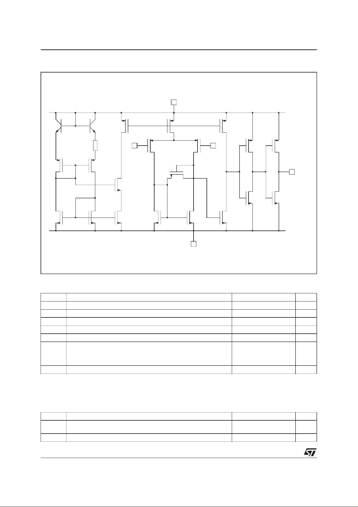
SCHEMATIC DIAGRAM (for 1/4 TS3704)
T
1
T
2
T
9
V+
CC
T
10
T
17
R
1
Input- Input+
TT
34
T
8
T
5
T
6
T
7
T
11
TT
14 15
T
12
T
13
T
16
V-
CC
TT
18 21
Output
TT
19 20
MAXIMUMRATINGS
Symbol Parameter Value Unit
+
V
V
V
T
T
Notes : 1. All voltage values, except differential voltage, are withrespect to networkground terminal.
Supply Voltage - (note1) 18 V
CC
DifferentialInput Voltage- (note 2) ±18 V
id
Input Voltage - (note3) 18 V
V
i
Output Voltage 18 V
O
Output Current 20 mA
I
O
Operating Free-Air TemperatureRange
oper
StorageTemperature Range -65 to +150
stg
2. Differentialvoltages are the non-invertinginput terminal withrespect to the inverting input terminal.
3. The magnitude of the inputand the outputvoltages mustnever exceed the magnitude of the positive supply voltage.
4. Short circuitfrom outputs to V
+
can cause excessive heating and eventual destruction.
CC
TS3704C
TS3704I
TS3704M
0 to +70
-40 to +125
-55 to +125
o
C
o
C
OPERATINGCONDITIONS
Symbol Parameter Value Unit
+
2/6
V
V
Supply Voltage TS3704C,I
CC
Common Mode Input VoltageRange 0 to V
icm
TS3704M
3to16
4to16
+
-1.5 V
CC
V
TS3704C,I,M
ELECTRICAL CHARACTERISTICS
+
= 5V, V
V
CC
Symbol Parameter Min. Typ. Max. Unit
V
io
I
io
I
ib
V
icm
CMR Common-mode Rejection Ratio
SVR Supply Voltage Rejection Ratio
V
OH
V
OL
I
CC
t
PLH
t
PHL
t
f
Note : 1. The specified offset voltage is the maximun value required to drive the output up to 4.5V or down to 0.3V.
2. Maximum values including unavoidable inaccuracies of the industrial test.
-
= 0V, T
CC
Input Offset Voltage
V
ic=vicm min.,VCC
T
≤ T
min.
amb
=25°C (unlessotherwisespecified)
amb
+
= 5V to 10V - (note 1)
≤T
.
max
Input Offset Current - (note 2)
= 2.5 V
V
ic
T
≤ T
≤T
min.
amb
max
.
Input Bias Current - (note 2)
= 2.5 V
V
ic
T
≤ T
≤T
min.
amb
max
.
Input Common Mode VoltageRange
T
≤ T
≤T
min.
amb
V
ic=Vicm min
+
V
= +5V to +10V 92
CC
.
max
.78
High Level Output Voltage
V
id
T
min.
=1V,I
≤ T
amb
OH =
≤T
-4mA
max
.
Low Level Output Voltage
V
id
T
min.
= -1V,I
≤ T
amb
OL =
≤T
4mA
max
.
Supply Current (4 comparators)
No load - Outputs low
≤ T
≤T
T
min.
amb
max
.
Response Time Low to High
= 0V,f = 10kHz, CL= 50pF, Overdrive= 5mV
V
ic
Overdrive = 10mV
Overdrive = 20mV
Overdrive = 40mV
TTLInput
Response Time High to Low
= 0V,f = 10kHz, CL= 50pF, Overdrive= 5mV
V
ic
Overdrive = 10mV
Overdrive = 20mV
Overdrive = 40mV
TTLInput
Fall time
f = 10kHz, C
= 50pF,Overdrive 50mV 30
L
0toV
0toV
CC
CC
4.5
4.3
+
+
1.2 5
6.5
1
300
1
600
-1.2
-1.5
4.7
234 300
375
36 80
100
1.2
1
0.9
0.8
0.7
2
1.5
0.9
0.7
0.15
mV
pA
pA
V
dB
dB
V
mV
µA
µs
µs
ns
3/6
 Loading...