

Datasheet TS3702IN, TS3702ID, TS3702I, TS3702CN, TS3702CD Datasheet (SGS Thomson Microelectronics)
...Page 1
MICROPOWER DUALCMOS VOLTAGE COMPARATORS
.
PUSH-PULL CMOS OUTPUT (NO EXTERNALPULL-UPRESISTORREQUIRED)
.
EXTREMELY LOW SUPPLY CURRENT :
9µATYP / COMPARATOR
.
WIDE SINGLE SUPPLYRANGE (3V TO 16V)
ORDUAL SUPPLIES (± 1.5V TO ± 8V)
.
EXTREMELY LOW INPUT BIAS CURRENT :
1pATYP
.
EXTREMELY LOW INPUT OFFSET
CURRENT : 1pATYP
.
INPUT COMMON-MODE VOLTAGE RANGE
INCLUDESGND
.
HIGH INPUT IMPEDANCE : 1012Ω TYP
.
FASTRESPONSETIME : 2µs TYP FOR 5mV
OVERDRIVE
.
PIN-TO-PIN AND FUNCTIONALLY COMPATIBLE WITH BIPOLAR LM393
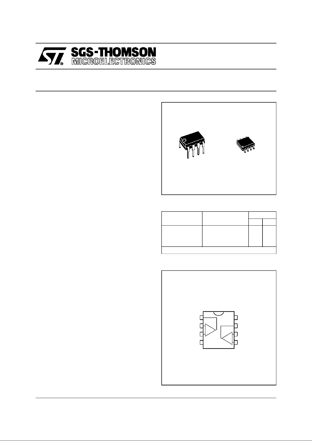
TS3702C,I,M
N
DIP8
(Plastic Package)
ORDERCODES
Part Number
TS3702C 0
TS3702I -40oC, +125oC ●●
TS3702M -55oC, +125oC ●●
Example : TS3702CN
(Plastic Micropackage)
Temperature
Range
o
C, +70oC ●●
D
SO8
Package
ND
DESCRIPTION
The TS3702 is a micropowerCMOS dual voltage
comparator with extremely low consumption of
9µA typ / comparator (20 times less than bipolar
LM393). The push-pull CMOSoutput stage allows
powerandspacesavingbyeliminatingthe external
pull-up resistor required by usual open-collector
output comparators.
Thusresponse times remain similar to the LM393.
October 1997
PIN CONNECTIONS (top view)
1
Output 1
InvertingInput 1
Non-invertingInput 1
2
-
+
3
-
V
45
CC
+
+
8
V
CC
7
Output2
6
InvertingInput 2
-
Non-invertingInput 2
1/5
Page 2
TS3702C,I,M
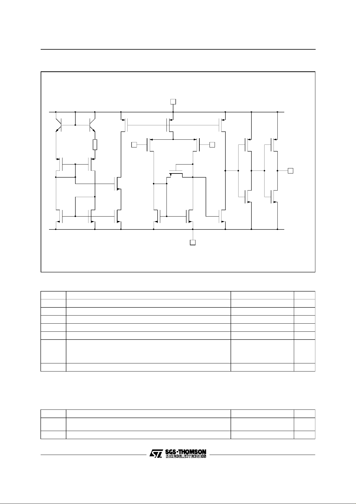
SCHEMATIC DIAGRAM (for 1/2TS3702)
T
1
T
2
T
9
V+
CC
T
10
T
17
R
1
Input- Input+
TT
34
T
8
T
5
T
6
T
7
T
11
TT
14 15
T
12
T
13
T
16
V-
CC
TT
18 21
Output
TT
19 20
MAXIMUM RATINGS
Symbol Parameter Value Unit
+
V
V
V
T
T
Notes : 1. All voltage values, except differential voltage, are with respect to network ground terminal.
Supply Voltage- (note 1) 18 V
CC
Differential Input Voltage - (note 2) ±18 V
id
Input Voltage - (note 3) 18 V
V
i
Output Voltage 18 V
O
Output Current 20 mA
I
O
Operating Free-Air Temperature Range
oper
Storage Temperature Range -65 to +150
stg
2. Differential voltages are the non-inverting input terminal with respect tothe inverting input terminal.
3. The magnitude of the input and the output voltagesmust never exceed themagnitude of the positive supply voltage.
4. Short circuit from outputs to V
+
can cause excessive heating and eventual destruction.
CC
TS3702C
TS3702I
TS3702M
0 to +70
-40 to +125
-55 to +125
o
C
o
C
OPERATING CONDITIONS
Symbol Parameter Value Unit
+
2/5
V
V
Supply Voltage TS3702C,I
CC
Common Mode Input Voltage Range 0 to V
icm
TS3702M
3to16
4to16
+
-1.5 V
CC
V
Page 3

TS3702C,I,M
ELECTRICAL CHARACTERISTICS
+
=5V, V
V
CC
Symbol Parameter Min. Typ. Max. Unit
V
io
I
io
I
ib
V
icm
CMR Common-mode Rejection Ratio
SVR Supply VoltageRejection Ratio
V
OH
V
OL
I
CC
t
PLH
t
PHL
t
f
Note : 1. The specified offset voltage is the maximun value required to drive the output up to 4.5Vor down to 0.3V.
2. Maximum valuesincluding unavoidable inaccuracies of the industrial test.
-
= 0V, T
CC
Input Offset Voltage
V
ic=Vicm min.,VCC
T
≤ T
min.
amb
=25°C (unlessotherwise specified)
amb
+
= 5V to 10V - (note 1)
≤ T
.
max
Input Offset Current - (note 2)
= 2.5 V
V
ic
T
≤ T
≤ T
min.
amb
max
.
Input Bias Current - (note 2)
= 2.5 V
V
ic
T
≤ T
≤ T
min.
amb
max
.
Input Common Mode Voltage Range
T
≤ T
≤ T
min.
amb
V
ic=Vicm min
+
V
= +5V to +10V 90
CC
.
max
.82
High Level Output Voltage
V
T
=1V,I
id
min.
≤ T
amb
OH =
≤ T
-4mA
max
.
Low Level Output Voltage
V
T
= -1V,I
id
min.
≤ T
amb
OL=
≤ T
4mA
max
.
Supply Current (2 comparators)
No load - Outputs low
≤ T
≤ T
T
min.
amb
max
.
Response Time Low to High
= 0V, f = 10kHz, CL= 50pF, Overdrive = 5mV
V
ic
Overdrive = 10mV
Overdrive = 20mV
Overdrive = 40mV
TTL Input
Response Time High to Low
= 0V, f = 10kHz, CL= 50pF, Overdrive = 5mV
V
ic
Overdrive = 10mV
Overdrive = 20mV
Overdrive = 40mV
TTLInput
Fall time
f = 10kHz, C
= 50pF,Overdrive 50mV 30
L
0toV
0toV
CC
CC
4.5
4.3
+
+
1.2 5
6.5
1
300
1
600
-1.2
-1.5
4.7
220 300
375
18 40
50
1.5
1.1
0.9
0.7
0.6
2.2
1.6
1.1
0.75
0.17
mV
pA
pA
V
dB
dB
V
mV
µA
µs
µs
ns
3/5
Page 4

TS3702C,I,M
PACKAGE MECHANICAL DATA
8 PINS - PLASTICDIP
Dimensions
Min. Typ. Max. Min. Typ. Max.
Millimeters Inches
A 3.32 0.131
a1 0.51 0.020
B 1.15 1.65 0.045 0.065
b 0.356 0.55 0.014 0.022
b1 0.204 0.304 0.008 0.012
D 10.92 0.430
E 7.95 9.75 0.313 0.384
e 2.54 0.100
e3 7.62 0.300
e4 7.62 0.300
F 6.6 0260
i 5.08 0.200
L 3.18 3.81 0.125 0.150
Z 1.52 0.060
PM-DIP8.EPS
DIP8.TBL
4/5
Page 5

PACKAGE MECHANICAL DATA
8 PINS - PLASTICMICROPACKAGE(SO)
TS3702C,I,M
Dimensions
Min. Typ. Max. Min. Typ. Max.
Millimeters Inches
A 1.75 0.069
a1 0.1 0.25 0.004 0.010
a2 1.65 0.065
a3 0.65 0.85 0.026 0.033
b 0.35 0.48 0.014 0.019
b1 0.19 0.25 0.007 0.010
C 0.25 0.5 0.010 0.020
c1 45
o
(typ.)
D 4.8 5.0 0.189 0.197
E 5.8 6.2 0.228 0.244
e 1.27 0.050
e3 3.81 0.150
F 3.8 4.0 0.150 0.157
L 0.4 1.27 0.016 0.050
M 0.6 0.024
S8
Information furnished is believed to be accurate and reliable. However, SGS-THOMSON Microelectronics assumes no responsibility
for the consequences of use of such information norfor anyinfringement of patents or other rights of third parties which may result
from itsuse. No license isgranted by implicationor otherwise under any patentor patent rightsof SGS-THOMSON Microelectronics.
Specification mentioned in this publication are subject to change without notice. This publication supersedes and replaces all
information previously supplied. SGS-THOMSON Microelectronics products are not authorized for use as critical components in life
support devices or systems without express written approval of SGS-THOMSON Microelectronics.
o
(max.)
PM-SO8.EPS
SO8.TBL
1997 SGS-THOMSON Microelectronics – Printed in Italy – All Rights Reserved
SGS-THOMSON Microelectronics GROUP OF COMPANIES
Australia - Brazil - Canada - China - France - Germany - Hong Kong - Italy - Japan - Korea - Malaysia - Malta - Morocco
The Netherlands - Singapore - Spain - Sweden - Switzerland - Taiwan - Thailand - United Kingdom -U.S.A.
ORDER CODE :
5/5
 Loading...