

查询TS339供应商
MICROPOWER QUAD CMOS VOLTAGE COMPARATORS
.
EXTREMELYLOW SUPPLYCURRENT :
9µATYP / COMPARATOR
.
WIDE SINGLE SUPPLY RANGE (3V TO 16V)
OR DUAL SUPPLIES(±1.5V TO
.
EXTREMELY LOW INPUT BIAS CURRENT :
1pA TYP
.
EXTREMELYLOW INPUTOFFSET
CURRENT: 1pATYP
.
INPUT COMMON-MODE VOLTAGE RANGE
INCLUDESGND
.
HIGHINPUT IMPEDANCE: 1012Ω TYP
.
FASTRESPONSETIME : 1.5µs TYP FOR
5mV OVERDRIVE
.
PIN-TO-PINAND FUNCTIONALLY
COMPATIBLEWITH BIPOLAR LM339
±8V)
TS339C,I,M
N
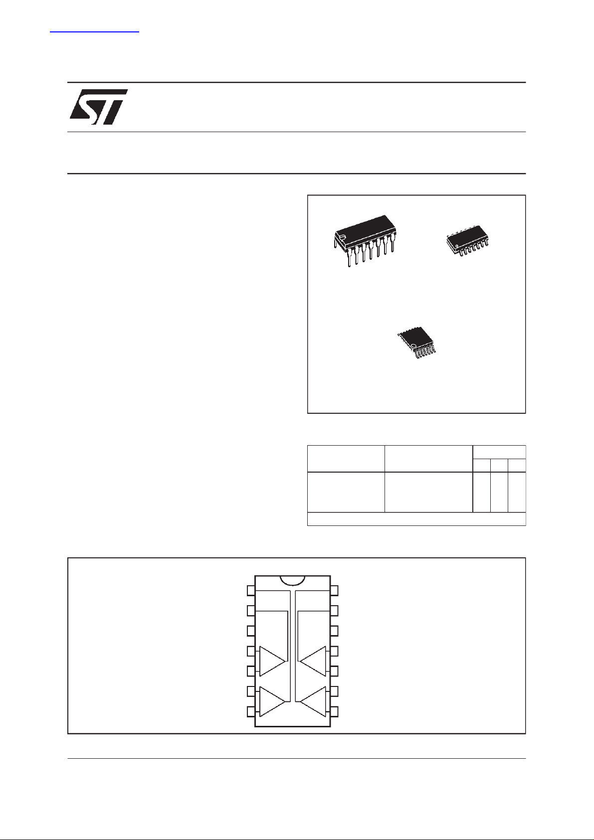
DIP14
(Plastic Package)
(Thin Shrink Small Outline Package)
(Plastic Micropackage)
P
TSSOP14
D
SO14
DESCRIPTION
The TS339 is a micropowerCMOS quad voltage
comparatorwith extremely low consumption of
9µA typ / comparator(20 times less than bipolar
LM339). Similar performancesare offered by the
quad micropowercomparatorTS3704withapushpull CMOS output.
Thus responsetimes remain similarto the LM339.
PIN CONNECTIONS (top view)
Output 2
Output 1
Inverting Input1
Non-inverting Input1
Inverting Input 2
Non-inverting Input 2
1
2
V
3
CC
4
-
+-
5
6
-
+-
7
ORDER CODES
Package
NDP
-
Temperature
Range
o
C, +70oC ●●●
Part Number
TS339C 0
TS339I -40oC, +125oC ●●●
TS339M -55oC, +125oC ●●●
Example : TS339CN
14+Output 3
13
Output 4
V
12
CC
11
+
+
Non-inverting Input 4
10
Inverting Input 4
9
Non-inverting Input 3
8
Inverting Input 3
September 1998
1/6
TS339C,I,M
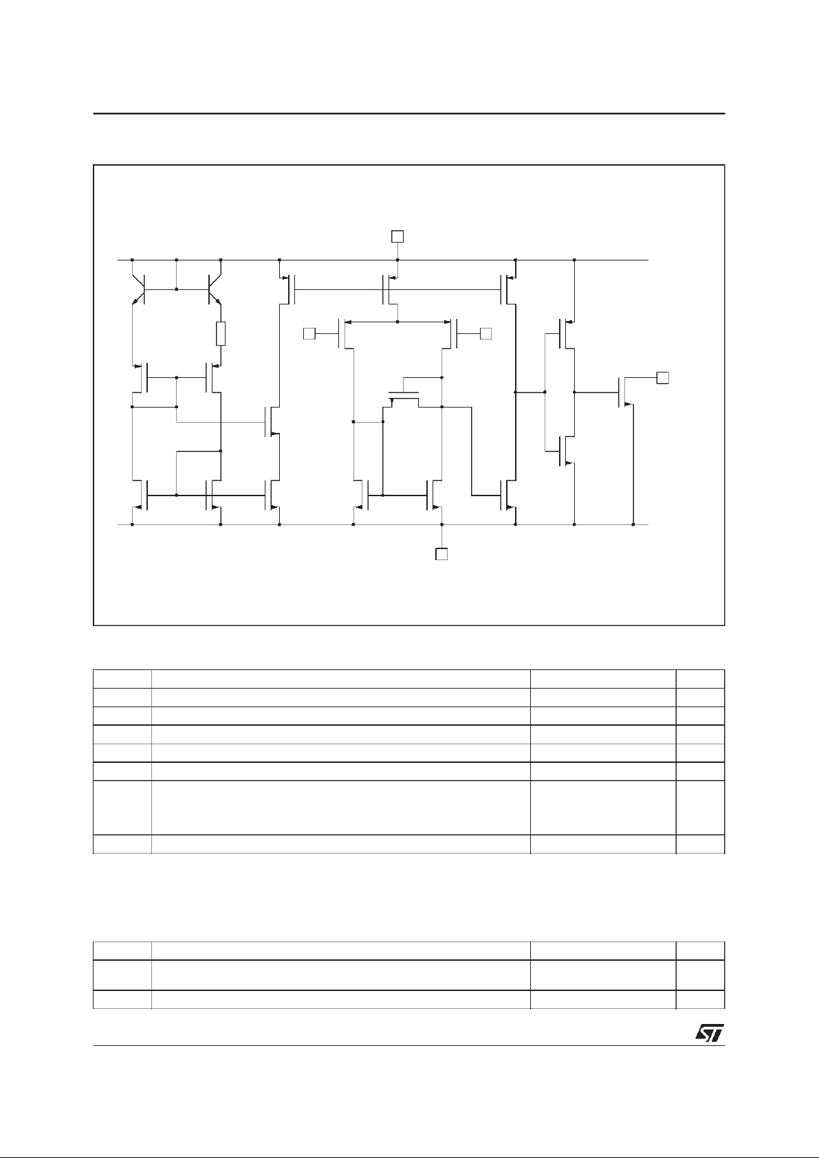
SCHEMATIC DIAGRAM (for 1/4 TS339)
T
1
T
2
T
9
V+
CC
T
10
T
17
R
1
Input - Input +
TT
34
T
8
T
5
T
6
T
7
T
11
TT
14 15
T
12
T
13
T
16
V-
CC
T
18
Output
T
20
T
19
MAXIMUMRATINGS
Symbol Parameter Value Unit
+
V
V
V
T
T
Notes : 1. Allvoltage values,except differential voltage, are with respect tonetwork ground terminal.
Supply Voltage- (note 1) 18 V
CC
Differential Input Voltage - (note2) ±18 V
id
Input Voltage- (note 3) 18 V
V
i
Output Voltage 18 V
O
Output Current 20 mA
I
O
Operating Free-Air TemperatureRange
oper
Storage TemperatureRange -65 to +150
stg
2. Differentialvoltages are the non-inverting input terminal withrespect to the inverting input terminal.
3. The magnitude of the input and the outputvoltages must never exceed the magnitude ofthe positive supplyvoltage.
4. Short circuit from outputs toV
+
can cause excessive heating andeventual destruction.
CC
TS339C
TS339I
TS339M
0 to +70
-40 to +125
-55 to +125
o
C
o
C
OPERATINGCONDITIONS
Symbol Parameter Value Unit
+
2/6
V
V
Supply Voltage TS339C,I
CC
Common Mode Input VoltageRange 0 to V
icm
TS339M
3to16
4to16
+
-1.5 V
CC
V

TS339C,I,M
ELECTRICAL CHARACTERISTICS
+
= 5V,V
V
CC
Symbol Parameter Min. Typ. Max. Unit
V
io
I
io
I
ib
V
icm
CMR Common-mode Rejection Ratio
SVR Supply VoltageRejection Ratio
I
OH
V
OL
I
CC
t
PLH
t
PHL
t
f
Note : 1. The specified offset voltage is the maximun value required todrive the output up to 4.5V or down to 0.3V.
2. Maximum valuesincluding unavoidableinaccuracies of the industrial test.
-
= 0V, T
CC
Input Offset Voltage- (note 1)
V
ic=Vicm min.,VCC
T
≤ T
min.
amb
=25°C (unlessotherwise specified)
amb
+
= 5V to 10V
≤T
.
max
Input Offset Current- (note 2)
= 2.5 V
V
ic
T
≤ T
≤T
min.
amb
max
.
Input Bias Current -(note 2)
= 2.5 V
V
ic
T
≤ T
≤T
min.
amb
max
.
Input Common Mode VoltageRange
T
≤ T
≤T
min.
amb
V
ic=Vicm min
+
V
= +5V to +10V 85
CC
.
max
.75
High Level Output Current
V
id
T
min.
=1V,V
≤ T
amb
OH =
≤T
+5V
max
.
Low Level Output Voltage
V
id
T
min.
= -1V,I
≤ T
amb
OL =
≤T
6mA
max
.
Supply Current (4comparators)
No load - Outputs low
≤ T
≤T
T
min.
amb
max
.
Response TimeLow to High
= 0V,f = 10kHz, RL= 5.1kΩ,CL= 15pF, Overdrive = 5mV
V
ic
Overdrive = 10mV
Overdrive = 20mV
Overdrive = 40mV
TTL Input
Response TimeHigh to Low
= 0V,f = 10kHz, RL= 5.1kΩ,CL= 15pF, Overdrive = 5mV
V
ic
Overdrive = 10mV
Overdrive = 20mV
Overdrive = 40mV
TTL Input
Fall Time
f = 10kHz, C
= 15pF, RL= 5.1kΩ, Overdrive 50mV 25
L
0toV
0toV
CC
CC
+
+
1.4 5
6.5
1
300
1
600
-1.2
-1.5
240
1000
350 400
650
36 80
100
1.5
1.2
1.1
0.9
0.8
2.5
1.9
1.2
0.8
0.08
mV
pA
pA
V
dB
dB
nA
mV
µA
µs
µs
ns
3/6

TS339C,I,M
PACKAGE MECHANICAL DATA
14 PINS - PLASTICDIP
Dimensions
Min. Typ. Max. Min. Typ. Max.
Millimeters Inches
a1 0.51 0.020
B 1.39 1.65 0.055 0.065
b 0.5 0.020
b1 0.25 0.010
D 20 0.787
E 8.5 0.335
e 2.54 0.100
e3 15.24 0.600
F 7.1 0.280
i 5.1 0.201
L 3.3 0.130
Z 1.27 2.54 0.050 0.100
PM-DIP14.EPS
DIP14.TBL
4/6

PACKAGE MECHANICAL DATA
14 PINS - PLASTICMICROPACKAGE (SO)
TS339C,I,M
Dimensions
Min. Typ. Max. Min. Typ. Max.
Millimeters Inches
A 1.75 0.069
a1 0.1 0.2 0.004 0.008
a2 1.6 0.063
b 0.35 0.46 0.014 0.018
b1 0.19 0.25 0.007 0.010
C 0.5 0.020
c1 45
o
(typ.)
D 8.55 8.75 0.336 0.334
E 5.8 6.2 0.228 0.244
e 1.27 0.050
e3 7.62 0.300
F 3.8 4.0 0.150 0.157
G 4.6 5.3 0.181 0.208
L 0.5 1.27 0.020 0.050
M 0.68 0.027
S8
o
(max.)
PM-SO14.EPS
SO14.TBL
5/6

TS339C,I,M
PACKAGE MECHANICAL DATA
14 PINS - THIN SHRINK SMALLOUTLINEPACKAGE
Dim.
Min. Typ. Max. Min. Typ. Max.
Millimeters Inches
A 1.20 0.05
A1 0.05 0.15 0.01 0.006
A2 0.80 1.00 1.05 0.031 0.039 0.041
b 0.19 0.30 0.007 0.15
c 0.09 0.20 0.003 0.012
D 4.90 5.00 5.10 0.192 0.196 0.20
E 6.40 0.252
E1 4.30 4.40 4.50 0.169 0.173 0.177
e 0.65 0.025
k0
o
o
8
o
0
o
8
l 0.50 0.60 0.75 0.09 0.0236 0.030
Information furnished is believed to be accurate and reliable. However, STMicroelectronics assumes no responsibility for the
consequences of use of such information nor for any infringement of patents or other rights of third parties which may result from
its use. No license is granted by implication or otherwise under any patent or patent rights of STMicroelectronics. Specifications
mentioned in this publication are subject to change without notice. This publication supersedes and replaces all information
previously supplied.STMicroelectronics productsare not authorized for use as criticalcomponents in life support devices orsystems
without express written approval of STMicroelectronics.
The ST logo isa trademark of STMicroelectronics
6/6
1998 STMicroelectronics– Printed in Italy – All Rights Reserved
STMicroelectronics GROUP OF COMPANIES
Australia- Brazil - Canada - China- France - Germany - Italy -Japan - Korea - Malaysia - Malta - Mexico -Morocco
The Netherlands - Singapore - Spain - Sweden - Switzerland- Taiwan- Thailand -United Kingdom - U.S.A.
ORDERCODE:

WWW.ALLDATASHEET.COM
Copyright © Each Manufacturing Company.
All Datasheets cannot be modified without permission.
This datasheet has been download from :
www.AllDataSheet.com
100% Free DataSheet Search Site.
Free Download.
No Register.
Fast Search System.
www.AllDataSheet.com
 Loading...