

Page 1
Micropower low-voltage rail-to-rail comparators
Features
■ Supply operation from 1.6 to 5 V
■ Low current consumption: 20 μA
■ Rail-to-rail inputs
■ Wide temperature range: -40°C to +125°C
■ Low output saturation voltage
■ Low propagation delay: 210 ns
■ Open-drain output
■ ESD tolerance: 2 kV HBM/200 V MM
■ SMD packages
Applications
■ Mobile phones
■ Notebooks and PDAs
■ Battery supplied electronics
■ General-purpose portable devices
■ General-purpose low voltage applications
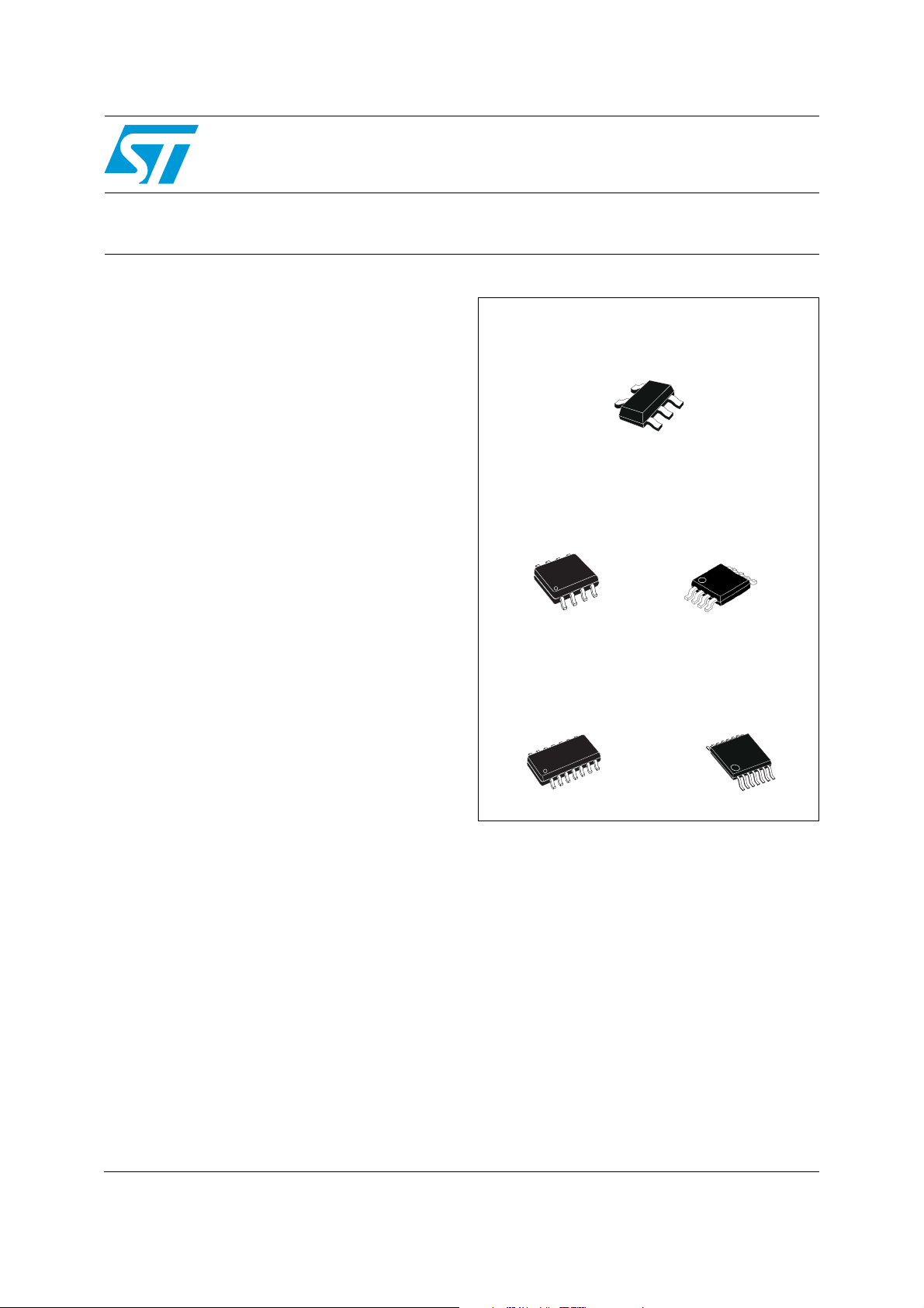
TS331, TS332, TS334
TS331
SOT23-5 / SC70-5
TS332
SO8 / MiniSO8
TS334
SO14 / TSSOP14
Description
The TS331, TS332 and TS334 are single, dual
and quad micropower and low-voltage
comparators. They can operate with a supply
voltage ranging from 1.6 to 5 V with a typical
current consumption as low as 20 μA. In addition,
rail-to-rail inputs make them a perfect choice for
low-voltage applications.
Their availability in tiny packages is a real
advantage for space saving constraints.
The TS33x are specified for a wide temperature
range of -40°C to +125°C, making them ideal for a
wide range of applications.
December 2011 Doc ID 17272 Rev 2 1/21
www.st.com
21
Page 2
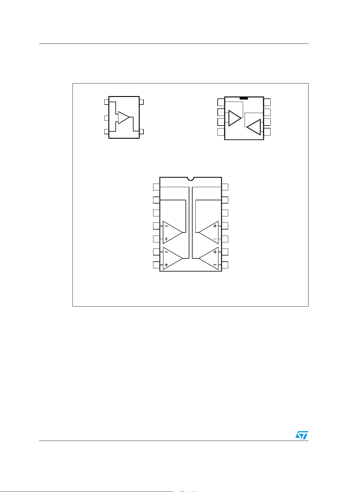
Package pin connections TS331, TS332, TS334
1 Package pin connections
Figure 1. Pin connections for each package (top view)
IN +
1
+
2
VCC -
IN -
-
3
TS331
SOT23-5 / SC70-5
VCC +
5
4OUT
OUT2
OUT1
VCC+
IN1-
IN1+
IN2-
IN2+
Out1
Out1
In1-
In1-
In1+
In1+
V
V
CC-
CC-
1
1
_
_
2
2
+
+
3
3
4
4
8
8
V
V
CC+
CC+
7
7
Out2
Out2
_
_
+
+
In2-
In2-
6
6
In2+
In2+
5
5
TS332
SO-8 / MiniSO-8
1
2
3
4
5
6
14
OUT3
13
OUT4
12
VCC -
11
IN4+
10
IN4-
9
IN3+
87
IN3-
TS334
SO-14 / TSSOP14
2/21 Doc ID 17272 Rev 2
Page 3
TS331, TS332, TS334 Absolute maximum ratings and operating conditions
2 Absolute maximum ratings and operating conditions
Table 1. Absolute maximum ratings
Symbol Parameter Value Unit
V
V
V
V
R
R
T
T
LEAD
ESD
CC
out
thja
thjc
stg
T
Supply voltage
ID
IN
Differential input voltage ± 5.5 V
Input voltage range (VCC-) -0.3 to (VCC+) + 0.3 V
Output voltage
Thermal resistance junction to ambient
SC70-5
SOT23-5
SO8
MiniSO8
SO14
TSSOP14
Thermal resistance junction to case
SC70-5
SOT23-5
SO8
MiniSO8
SO14
TSSOP14
Storage temperature -65 to +150 °C
j
Junction temperature 150 °C
Lead temperature (soldering 10 seconds) 260 °C
Human body model (HBM)
Charged device model (CDM)
Latch-up immunity 200 mA
(1)
(1)
(4)
(3)
(5)
(2)
(2)
5.5 V
5.5 V
205
250
125
190
105
100
172
81
40
39
31
32
2000
200
1500
°C/W
°C/W
VMachine model (MM)
1. All voltage values, except differential voltage, are referenced to Vcc-.
2. Short-circuits can cause excessive heating. These values are typical.
3. Human body model: a 100 pF capacitor is charged to the specified voltage, then discharged through a
1.5 kΩ resistor between two pins of the device. This is done for all couples of connected pin combinations
while the other pins are floating.
4. Machine model: a 200 pF capacitor is charged to the specified voltage, then discharged directly between
two pins of the device with no external series resistor (internal resistor < 5 Ω). This is done for all couples of
connected pin combinations while the other pins are floating.
5. Charged device model: all pins and package are charged together to the specified voltage and then
discharged directly to ground through only one pin. This is done for all pins.
Doc ID 17272 Rev 2 3/21
Page 4

Absolute maximum ratings and operating conditions TS331, TS332, TS334
Table 2. Operating conditions
Symbol Parameter Value Unit
T
V
V
oper
CC
ICM
Operating temperature range -40 to +125 °C
Supply voltage (VCC+) - (VCC-)
-40°C < T
< +125°C 1.6 to 5.0
amb
Common mode input voltage range
T
= +25°C
amb
-40°C < T
< +125°C
amb
(VCC-) -0.2 to (VCC+)+0.2
(VCC-) to (VCC+)
V
V
4/21 Doc ID 17272 Rev 2
Page 5
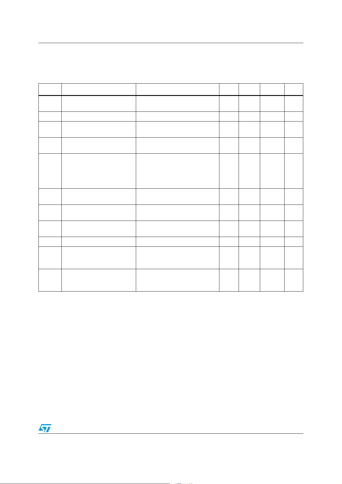
TS331, TS332, TS334 Electrical characteristics
3 Electrical characteristics
Table 3. VCC+=+1.8V, VCC-=0V, T
= +25°C (unless otherwise specified)
amb
Symbol Parameter Test conditions Min. Typ. Max. Unit
V
Input offset voltage
IO
ΔV
I
Input offset voltage drift -40°C < T
IO
I
Input bias current
IB
I
Input offset current
IO
I
Supply current
CC
I
Output current leakage
OH
V
Output voltage low
OL
Output sink current
SINK
(1)
(1)
CMRR Common mode rejection ratio 0 < V
TP
TP
1. Maximum values include unavoidable inaccuracies of the industrial tests.
2. TP
3. TP
Propagation delay
HL
High to low output level
Propagation delay
LH
Low to high output level
is measured when the output signal crosses a voltage level at 50% of Vcc with the following conditions: inverting input
HL
voltage (IN-) = VICM and non-inverting input voltage (IN+) moving from VICM + 100 mV to VICM - overdrive.
is measured when the output signal crosses a voltage level at 50% of Vcc with the following conditions: inverting input
LH
voltage (IN-) = VICM and non-inverting input voltage (IN+) moving from VICM - 100 mV to VICM + overdrive.
(2)
(3)
-40°C < T
-40°C < T
-40°C < T
No load, output low, V
-40°C < T
< +125°C
amb
< +125°C 4.5 μV/°C
amb
< +125°C
amb
< +125°C
amb
< +125°C
amb
ICM
No load, output high, V
-40°C < T
V
OUT=VCC
-40°C < T
= 1 mA
I
SINK
-40°C < T
= 1.5 V
V
OUT
-40°C < T
ICM
=0V, RL = 5.1 kΩ, CL = 50 pF
V
ICM
< +125°C
amb
+
< +125°C
amb
< +125°C
amb
< +125°C
amb
< 1.8 V 50 68 dB
Overdrive = 10 mV
Overdrive = 100 mV
= 0 V, RL = 5.1 kΩ, CL = 50 pF
V
ICM
Overdrive = 10 mV
Overdrive = 100 mV
ICM
=0V
=0V
20
15
0.5 5
6
25 40
100
110
100
20
26
30
22
29
33
110
500
24 30
50
22
300
210 310
540
420 620
mV
nA
nA
μA
nA
mV
mA
ns
ns
Doc ID 17272 Rev 2 5/21
Page 6
Electrical characteristics TS331, TS332, TS334
Table 4. VCC+=+2.7V, VCC-=0V, T
= +25°C (unless otherwise specified)
amb
Symbol Parameter Test conditions Min. Typ. Max. Unit
V
Input offset voltage
IO
ΔV
I
Input offset voltage drift -40°C < T
IO
I
Input bias current
IB
I
Input offset current
IO
Supply current
I
CC
I
Output current leakage
OH
V
Output voltage low
OL
Output sink current
SINK
(1)
(1)
CMRR Common mode rejection ratio
TP
Propagation delay
HL
High to low output level
(2)
-40°C < T
-40°C < T
-40°C < T
No load, output low, V
-40°C < T
< +125°C
amb
< +125°C 3.3 μV/°C
amb
< +125°C
amb
< +125°C
amb
< +125°C
amb
ICM
No load, output high, V
-40°C < T
V
OUT=VCC
-40°C < T
I
= 1 mA
SINK
-40°C < T
= 1.5 V
V
OUT
-40°C < T
0 < V
ICM
-40°C < T
=0V, RL=5.1kΩ, CL=50pF
V
ICM
< +125°C
amb
+
< +125°C
amb
< +125°C
amb
< +125°C
amb
< 2.7 V
< +125°C
amb
Overdrive = 10 mV
Overdrive = 100 mV
ICM
= 0 V
=0V
40
30
54
53
0.5 5
6
25 40
100
110
100
21
27
31
23
30
34
110
500
17 30
50
47
74
320
220 320
mV
nA
nA
μA
nA
mV
mA
dB
ns
= 0 V, RL = 5.1 kΩ, CL = 50 pF
TP
1. Maximum values include unavoidable inaccuracies of the industrial tests.
2. TP
3. TP
Propagation delay
LH
Low to high output level
is measured when the output signal crosses a voltage level at 50% of Vcc with the following conditions: Inverting
HL
input voltage (IN-) = VICM and non-inverting input voltage (IN+) moving from VICM + 100 mV to VICM - overdrive.
is measured when the output signal crosses a voltage level at 50% of Vcc with the following conditions: Inverting
LH
input voltage (IN-) = VICM and non-inverting input voltage (IN+) moving from VICM - 100 mV to VICM + overdrive.
(3)
V
ICM
Overdrive = 10 mV
Overdrive = 100 mV
550
420 640
ns
6/21 Doc ID 17272 Rev 2
Page 7
TS331, TS332, TS334 Electrical characteristics
Table 5. VCC+ = +5 V, VCC- = 0 V, T
= +25°C (unless otherwise specified)
amb
Symbol Parameter Test conditions Min. Typ. Max. Unit
V
Input offset voltage
IO
ΔV
I
Input offset voltage drift -40°C < T
IO
I
Input bias current
IB
I
Input offset current
IO
Supply current
I
CC
I
Output current leakage
OH
V
Output voltage low
OL
Output sink current
SINK
A
Voltage gain 40 100 V/mV
V
(1)
(1)
CMRR Common mode rejection ratio
SVR Supply voltage rejection
TP
Propagation delay
HL
High to low output level
(2)
-40°C < T
-40°C < T
-40°C < T
No load, output low, V
-40°C < T
< +125°C
amb
< +125°C 1.3 μV/°C
amb
< +125°C
amb
< +125°C
amb
< +125°C
amb
ICM
No load, output high, V
-40°C < T
V
OUT
-40°C < T
I
= 4 mA
SINK
-40°C < T
= 1.5 V
V
OUT
-40°C < T
0 < V
ICM
-40°C < T
ΔV
CC
-40°C < T
= 0 V, RL = 5.1 kΩ, CL = 50 pF
V
ICM
< +125°C
amb
= VCC+
< +125°C
amb
< +125°C
amb
< +125°C
amb
< 5 V
< +125°C
amb
= 1.8 to 5 V
< +125°C
amb
Overdrive = 10 mV
Overdrive = 100 mV
ICM
= 0 V
= 0 V
82
60
60
58
56
56
0.5 5
6
30 40
100
110
100
23
30
34
26
34
38
110
600
48 60
80
93
79
75
380
270 430
mV
nA
nA
μA
nA
mV
mA
dB
dB
ns
= 0 V, RL = 5.1 kΩ, CL = 50 pF
TP
1. Maximum values include unavoidable inaccuracies of the industrial tests.
2. TP
3. TP
Propagation delay
LH
Low to high output level
is measured when the output signal crosses a voltage level at 50% of Vcc with the following conditions: Inverting
HL
input voltage (IN-) = VICM and non-inverting input voltage (IN+) moving from VICM + 100 mV to VICM - overdrive.
is measured when the output signal crosses a voltage level at 50% of Vcc with the following conditions: Inverting
LH
input voltage (IN-) = VICM and non-inverting input voltage (IN+) moving from VICM - 100 mV to VICM + overdrive.
(3)
V
ICM
Overdrive = 10 mV
Overdrive = 100 mV
570
450 720
Doc ID 17272 Rev 2 7/21
ns
Page 8

Electrical characteristics TS331, TS332, TS334
Figure 2. Supply current versus supply
voltage with output high,
V
= 0 V
ICM
Figure 4. Supply current versus supply
voltage with output low,
V
= 0 V
ICM
Figure 3. Supply current versus supply
voltage with output high,
V
= V
ICM
CC
Figure 5. Supply current versus supply
voltage with output low,
V
= V
ICM
CC
Figure 6. Supply current versus temperature Figure 7. Input bias current versus input
common-mode voltage
8/21 Doc ID 17272 Rev 2
Page 9

TS331, TS332, TS334 Electrical characteristics
Figure 8. Input current versus differential
input voltage
Figure 10. Output voltage versus output sink
current, V
= 1.8 V
CC
Figure 9. Input offset voltage versus
temperature
Figure 11. Output voltage versus output sink
current, VCC = 2.7 V
Figure 12. Output voltage versus output sink
current, V
CC
= 5 V
Figure 13. Output sink current versus output
voltage
Doc ID 17272 Rev 2 9/21
Page 10

Electrical characteristics TS331, TS332, TS334
Figure 14. Output voltage versus temperature Figure 15. Propagation delay versus overdrive
Figure 16. Propagation delay versus overdrive
with positive transition, V
= 1.8 V
CC
with negative transition, V
Figure 17. Propagation delay versus common
mode voltage, VCC = 1.8 V
= 1.8 V
CC
Figure 18. Propagation delay versus overdrive
with negative transition, V
= 2.7 V
CC
Figure 19. Propagation delay versus overdrive
with positive transition, VCC = 2.7 V
10/21 Doc ID 17272 Rev 2
Page 11

TS331, TS332, TS334 Electrical characteristics
Figure 20. Propagation delay versus common
mode voltage, V
= 2.7 V
CC
Figure 22. Propagation delay versus overdrive
with positive transition, V
CC
= 5 V
Figure 21. Propagation delay versus overdrive
with negative transition, VCC = 5 V
Figure 23. Propagation delay versus common
mode voltage, VCC = 5 V
Figure 24. Propagation delay versus time with
negative transition
Figure 25. Propagation delay versus time with
positive transition
Doc ID 17272 Rev 2 11/21
Page 12

Package information TS331, TS332, TS334
4 Package information
In order to meet environmental requirements, ST offers these devices in different grades of
ECOPACK
specifications, grade definitions and product status are available at: www.st.com.
ECOPACK
®
packages, depending on their level of environmental compliance. ECOPACK®
®
is an ST trademark.
12/21 Doc ID 17272 Rev 2
Page 13

TS331, TS332, TS334 Package information
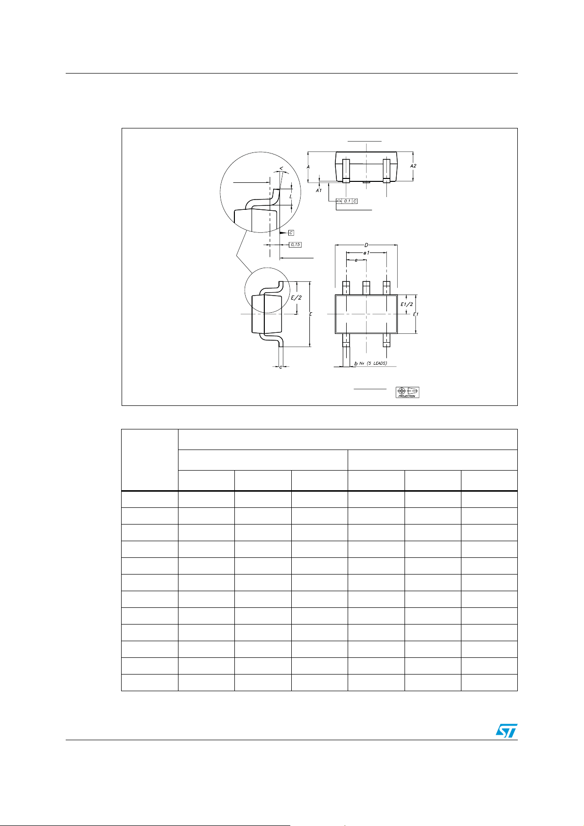
4.1 SOT23-5 package
Figure 26. SOT23-5 package mechanical drawing
Table 6. SOT23-5 package mechanical data
Dimensions
Ref.
Min. Typ. Max. Min. Typ. Max.
A 0.90 1.20 1.45 0.035 0.047 0.057
A1 0.15 0.006
A2 0.90 1.05 1.30 0.035 0.041 0.051
B 0.35 0.40 0.50 0.013 0.015 0.019
C 0.09 0.15 0.20 0.003 0.006 0.008
D 2.80 2.90 3.00 0.110 0.114 0.118
D1 1.90 0.075
e 0.95 0.037
E 2.60 2.80 3.00 0.102 0.110 0.118
F 1.50 1.60 1.75 0.059 0.063 0.069
L 0.10 0.35 0.60 0.004 0.013 0.023
K 0 degrees 10 degrees
Millimeters Inches
Doc ID 17272 Rev 2 13/21
Page 14
Package information TS331, TS332, TS334
4.2 SC70-5 (SOT323-5) package
Figure 27. SC70-5 (SOT323-5) package mechanical drawing
DIMENSIONS IN MM
GAUGE PLANE
SEATING PLANE
SIDE VIEW
COPLANAR LEADS
TOP VIEW
Table 7. SC70-5 (or SOT323-5) package mechanical data
Dimensions
Ref
Min Typ Max Min Typ Max
A 0.80 1.10 0.315 0.043
A1 0.10 0.004
A2 0.80 0.90 1.00 0.315 0.035 0.039
b 0.15 0.30 0.006 0.012
c 0.10 0.22 0.004 0.009
D 1.80 2.00 2.20 0.071 0.079 0.087
E 1.80 2.10 2.40 0.071 0.083 0.094
E1 1.15 1.25 1.35 0.045 0.049 0.053
e 0.65 0.025
e1 1.30 0.051
L 0.26 0.36 0.46 0.010 0.014 0.018
Millimeters Inches
<0° 8°
14/21 Doc ID 17272 Rev 2
Page 15

TS331, TS332, TS334 Package information
4.3 SO-8 package information
Figure 28. SO-8 package mechanical drawing
Table 8. SO-8 package mechanical data
Dimensions
Ref.
Min. Typ. Max. Min. Typ. Max.
A1.750.069
A1 0.10 0.25 0.004 0.010
A2 1.25 0.049
b 0.28 0.48 0.011 0.019
c 0.17 0.23 0.007 0.010
D 4.80 4.90 5.00 0.189 0.193 0.197
E 5.80 6.00 6.20 0.228 0.236 0.244
E1 3.80 3.90 4.00 0.150 0.154 0.157
e 1.27 0.050
h 0.25 0.50 0.010 0.020
L 0.40 1.27 0.016 0.050
L1 1.04 0.040
k 0 8° 1° 8°
Millimeters Inches
ccc 0.10 0.004
Doc ID 17272 Rev 2 15/21
Page 16

Package information TS331, TS332, TS334
4.4 MiniSO-8 package information
Figure 29. MiniSO-8 package mechanical drawing
Table 9. MiniSO-8 package mechanical data
Dimensions
Ref.
Min. Typ. Max. Min. Typ. Max.
A 1.1 0.043
A1 0 0.15 0 0.006
A2 0.75 0.85 0.95 0.030 0.033 0.037
b 0.22 0.40 0.009 0.016
c 0.08 0.23 0.003 0.009
D 2.80 3.00 3.20 0.11 0.118 0.126
E 4.65 4.90 5.15 0.183 0.193 0.203
E1 2.80 3.00 3.10 0.11 0.118 0.122
e 0.65 0.026
L 0.40 0.60 0.80 0.016 0.024 0.031
L1 0.95 0.037
L2 0.25 0.010
k0° 8°0° 8°
ccc 0.10 0.004
Millimeters Inches
16/21 Doc ID 17272 Rev 2
Page 17

TS331, TS332, TS334 Package information
4.5 SO-14 package information
Figure 30. SO-14 package mechanical drawing
Table 10. SO-14 package mechanical data
Dimensions
Millimeters Inches
Ref.
Min. Typ. Max. Min. Typ. Max.
A 1.35 1.75 0.05 0.068
A1 0.10 0.25 0.004 0.009
A2 1.10 1.65 0.04 0.06
B 0.33 0.51 0.01 0.02
C 0.19 0.25 0.007 0.009
D 8.55 8.75 0.33 0.34
E 3.80 4.0 0.15 0.15
e1.27 0.05
H 5.80 6.20 0.22 0.24
h 0.25 0.50 0.009 0.02
L 0.40 1.27 0.015 0.05
k 8° (max.)
ddd 0.10 0.004
Doc ID 17272 Rev 2 17/21
Page 18

Package information TS331, TS332, TS334
4.6 TSSOP14 package information
Figure 31. TSSOP14 package mechanical drawing
Table 11. TSSOP14 package mechanical data
Dimensions
Ref.
Min. Typ. Max. Min. Typ. Max.
A1.200.047
A1 0.05 0.15 0.002 0.004 0.006
A2 0.80 1.00 1.05 0.031 0.039 0.041
b 0.19 0.30 0.007 0.012
c 0.09 0.20 0.004 0.0089
D 4.90 5.00 5.10 0.193 0.197 0.201
E 6.20 6.40 6.60 0.244 0.252 0.260
E1 4.30 4.40 4.50 0.169 0.173 0.176
e 0.65 0.0256
L 0.45 0.60 0.75 0.018 0.024 0.030
L1 1.00 0.039
k0° 8°0° 8°
aaa 0.10 0.004
Millimeters Inches
18/21 Doc ID 17272 Rev 2
Page 19

TS331, TS332, TS334 Ordering information
5 Ordering information
Table 12. Order codes
Part number
TS331ILT
TS331ICT SC70-5 K55
TS332IDT SO8 332I
TS332IST MiniSO8 K507
TS334IDT SO14 334I
TS334IPT TSSOP14 334I
Temperature
range
-40°C, +125°C
Package Packaging Marking
SOT23-5
Tape & reel
K506
Doc ID 17272 Rev 2 19/21
Page 20

Revision history TS331, TS332, TS334
6 Revision history
Table 13. Document revision history
Date Revision Changes
29-Mar-2010 1 Initial release.
– Added TS332 and TS334 devices.
01-Dec-2011 2
– Added V
– Removed note "The magnitude of input and output voltages
must never exceed the supply rail ±0.3 V." from Ta b le 1 .
– Removed note "All values over the temperature range are
guaranteed through correlation and simulation. No production
tests have been performed at the temperature range limits."
from Ta b le 3 , Ta b le 4 and Ta bl e 5 .
– Removed "Vicm = 0 V" from Test conditions column in Tab l e 3,
Ta bl e 4 and Tab l e 5.
– Modified minimal Isink value in Ta b le 5 .
parameter in Table 1: Absolute maximum ratings.
out
20/21 Doc ID 17272 Rev 2
Page 21

TS331, TS332, TS334
Please Read Carefully:
Information in this document is provided solely in connection with ST products. STMicroelectronics NV and its subsidiaries (“ST”) reserve the
right to make changes, corrections, modifications or improvements, to this document, and the products and services described herein at any
time, without notice.
All ST products are sold pursuant to ST’s terms and conditions of sale.
Purchasers are solely responsible for the choice, selection and use of the ST products and services described herein, and ST assumes no
liability whatsoever relating to the choice, selection or use of the ST products and services described herein.
No license, express or implied, by estoppel or otherwise, to any intellectual property rights is granted under this document. If any part of this
document refers to any third party products or services it shall not be deemed a license grant by ST for the use of such third party products
or services, or any intellectual property contained therein or considered as a warranty covering the use in any manner whatsoever of such
third party products or services or any intellectual property contained therein.
UNLESS OTHERWISE SET FORTH IN ST’S TERMS AND CONDITIONS OF SALE ST DISCLAIMS ANY EXPRESS OR IMPLIED
WARRANTY WITH RESPECT TO THE USE AND/OR SALE OF ST PRODUCTS INCLUDING WITHOUT LIMITATION IMPLIED
WARRANTIES OF MERCHANTABILITY, FITNESS FOR A PARTICULAR PURPOSE (AND THEIR EQUIVALENTS UNDER THE LAWS
OF ANY JURISDICTION), OR INFRINGEMENT OF ANY PATENT, COPYRIGHT OR OTHER INTELLECTUAL PROPERTY RIGHT.
UNLESS EXPRESSLY APPROVED IN WRITING BY TWO AUTHORIZED ST REPRESENTATIVES, ST PRODUCTS ARE NOT
RECOMMENDED, AUTHORIZED OR WARRANTED FOR USE IN MILITARY, AIR CRAFT, SPACE, LIFE SAVING, OR LIFE SUSTAINING
APPLICATIONS, NOR IN PRODUCTS OR SYSTEMS WHERE FAILURE OR MALFUNCTION MAY RESULT IN PERSONAL INJURY,
DEATH, OR SEVERE PROPERTY OR ENVIRONMENTAL DAMAGE. ST PRODUCTS WHICH ARE NOT SPECIFIED AS "AUTOMOTIVE
GRADE" MAY ONLY BE USED IN AUTOMOTIVE APPLICATIONS AT USER’S OWN RISK.
Resale of ST products with provisions different from the statements and/or technical features set forth in this document shall immediately void
any warranty granted by ST for the ST product or service described herein and shall not create or extend in any manner whatsoever, any
liability of ST.
ST and the ST logo are trademarks or registered trademarks of ST in various countries.
Information in this document supersedes and replaces all information previously supplied.
The ST logo is a registered trademark of STMicroelectronics. All other names are the property of their respective owners.
© 2011 STMicroelectronics - All rights reserved
STMicroelectronics group of companies
Australia - Belgium - Brazil - Canada - China - Czech Republic - Finland - France - Germany - Hong Kong - India - Israel - Italy - Japan -
Malaysia - Malta - Morocco - Philippines - Singapore - Spain - Sweden - Switzerland - United Kingdom - United States of America
www.st.com
Doc ID 17272 Rev 2 21/21
 Loading...