

®
SMALL SIGNAL SC HO TTKY DIODE
DESCRIPTION
Metal to silicon junction diode featuring high breakdown, low turn-on voltage and ultrafast switching.
Primarly intended for high level U HF/VHF detection
and pulse application with broad dynamic range.
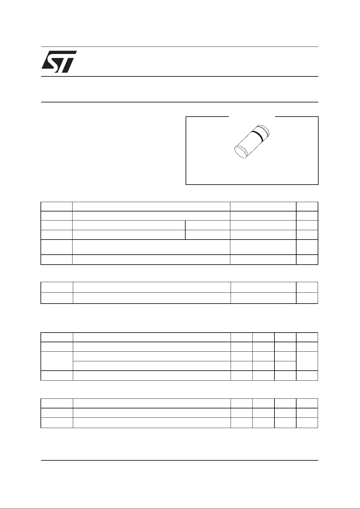
TMM 6263
MINIMELF
(Glass)
ABSOL UT E MAXIMUM RATING S
(limiting values)
Symbol Parameter Value Unit
V
I
FSM
T
RRM
I
F
stg
T
T
L
Repetitive Peak Reverse Voltage 60 V
Forward Continuous Current
Surge non Repetitive Forward Current
= 25 °C
T
i
≤ 1s
t
p
15 mA
50 mA
Storage and Junction Temperature Range - 65 to 200
j
-65 to 200
Maximum Temperature for Soldering during 15s 260
THERMAL RESISTANCE
Symbol Test Conditions Value Unit
R
th(j-l)
Junction-leads 400
ELECTRICAL CHARACT E RISTI CS
STATIC CHARACTERISTICS
Symbol Test Conditions Min. Typ. Max. Unit
V
BR
V
*
F
I
*
R
T
= 25°CI
amb
= 25°CI
T
amb
T
= 25°C IF = 15mA
amb
= 25°CV
T
amb
= 10µA
R
= 1mA
F
= 50V
R
60 V
0.41 V
1
0.2
C/W
°
µ
C
°
C
°
A
DYNAMIC CHARACTERI STICS
Symbol Test Conditions Min. Typ. Max. Unit
C
τ
* Pulse test: t
Matched batches availabl e on request. Test conditions (forward voltage and/or capacitan ce) accordi ng to customer specification.
T
= 25°CV
amb
T
= 25°CI
amb
300µs δ < 2%
≤
p
= 0V f = 1MHz
R
= 5mA Krakauer Method
F
.
August 1999 Ed: 1A
2.2 pF
100 ps
1/3
TMM 6263
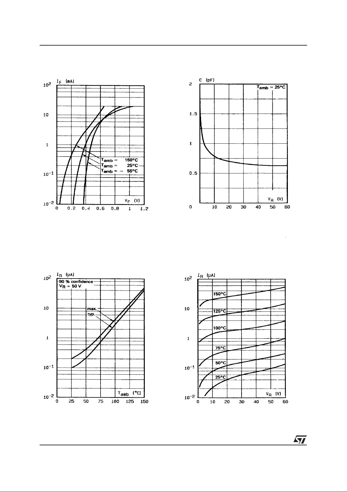
Figure 1. Forward current versus forward
voltage (typical values).
Figure 2. Capacitance C versus reverse
applied voltage V
(typical values).
R
Figure 3. Reverse current versus ambient
temperature.
Figure 4. Rever se current versus continuous
reverse voltage (typical values).
2/3

PACKAGE MECHANICAL DATA
MINIMELF Glass
TMM 6263
A
C
C
FOOT PRINT DIMENSIONS (Millimeter)
2.5
5
DIMENSIONS
REF.
Millimeters Inches
Min. Typ. Max. Min. Typ. Max.
B
/
O
A 3.30 3.40 3.6 0.130 0.134 0.142
B 1.59 1.60 1.62 0.063 0.063 0.064
C 0.40 0.45 0.50 0.016 0.018 0.020
D 1.50 0.059
2
Marking: ring at cathode end.
Weight: 0.05g
Information furnished is believed to be accurate and reliable. However, STMicroelectronics assumes no responsibility for the consequences of
use of such informat ion nor for any infringement of patents or other ri ghts of third par ties w hic h m ay res ul t fr om its use . No l i cense is granted
by implication or otherwise under any patent or patent rights of STMicroelectronics. Specifications mentioned in this publication are subject to
change without notice. This publication supersedes and replaces all information previously supplied.
STMicroelectronics products are not authorized for use as critical components in life support devices or systems without express written approval
of STMicroelectronic s.
The ST logo is a registered trademark of STMicroelectronics
© 1999 STMicroelectronics - Printed in Italy - All rights reserved.
STMicroelectronics GROUP OF COMPANIES
Australia - Brazil - China - Finland - France - Germany - Hong Kong - India - Italy - Japan - Malaysia
Malta - Morocco - Singapore - Spain - Sweden - Switzerland - United Kingdom - U.S.A.
http://www.st.com
3/3
 Loading...