

General purpose JFET dual operational amplifiers
Features
■ Wide common-mode (up to V
differential voltage range
■ Low input bias and offset current
■ Output short-circuit protection
■ High input impedance JFET input stage
■ Internal frequency compensation
■ Latch up free operation
■ High slew rate: 16 V/µs (typical)
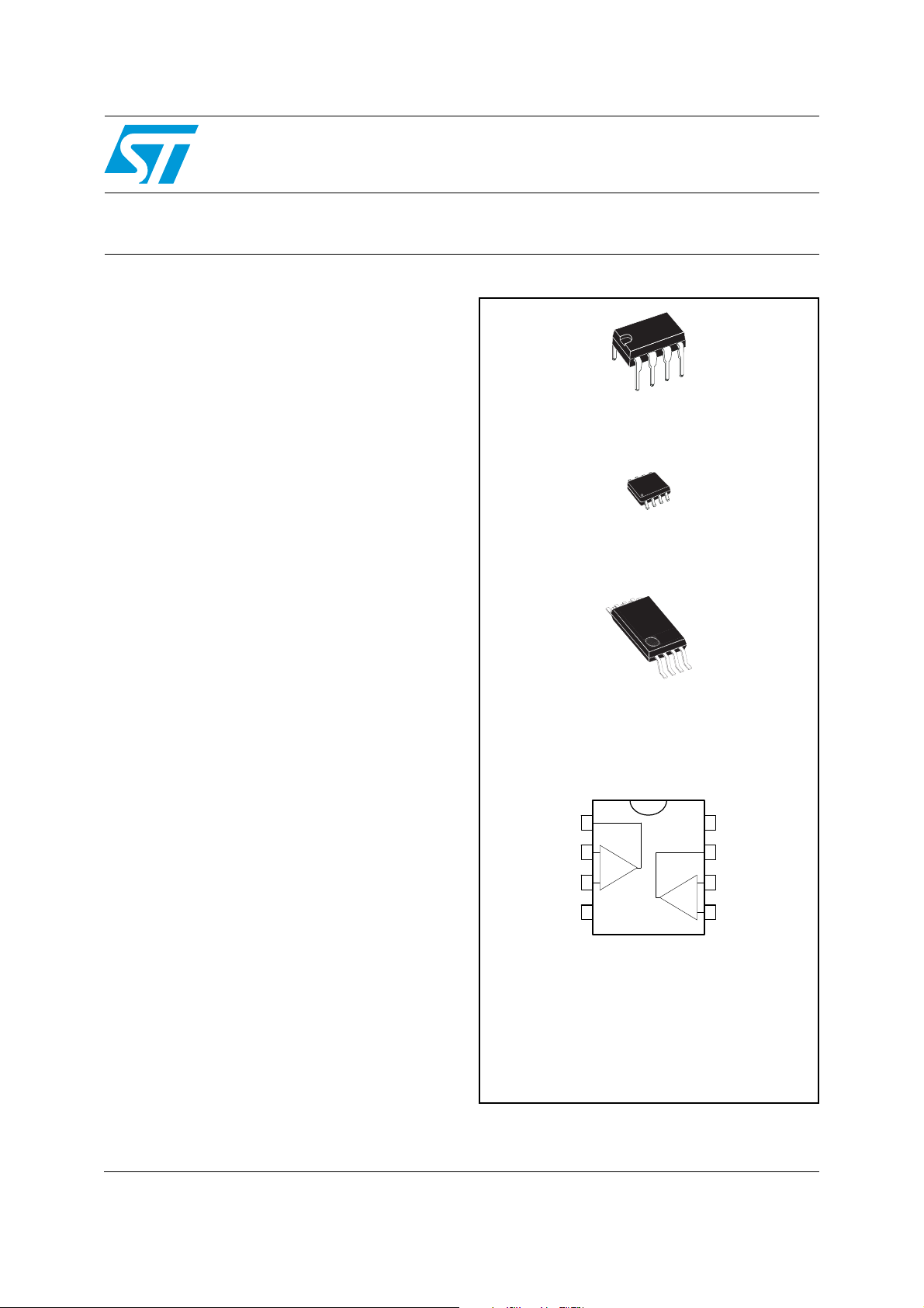
Description
The TL082, TL082A and TL082B are high speed
JFET input dual operational amplifiers
incorporating well matched, high voltage JFET
and bipolar transistors in a monolithic integrated
circuit.
CC
+
) and
TL082
TL082A TL082B
N
DIP8
(Plastic package)
D
SO-8
(Plastic micropackage)
The devices feature high slew rates, low input
bias and offset current, and low offset voltage
temperature coefficient.
P
TSSOP8
(Thin shrink small outline package)
Pin connections (top view)
1
2
-
+
3
45
8
7
6
-
+
1 - Output 1
2 - Inverting input 1
3 - Non-inverting input 1
4 - V
CC
-
5 - Non-inverting input 2
6 - Inverting input 2
7 - Output 2
8 - V
CC
+
June 2008 Rev 10 1/17
www.st.com
17
Schematic diagram TL082 TL082A TL082B
1 Schematic diagram
Figure 1. Schematic diagram
V
CC
Non-inverting
input
Inverting
input
30k
100
100
Ω
Ω
200
Ω
Output
1/2 TL082
8.2k
Ω
1.3k
35k
V
CC
1.3k
35k
100
2/17
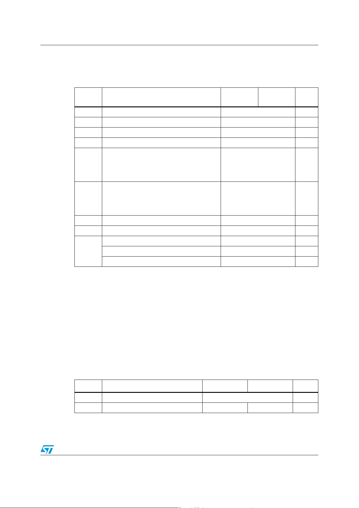
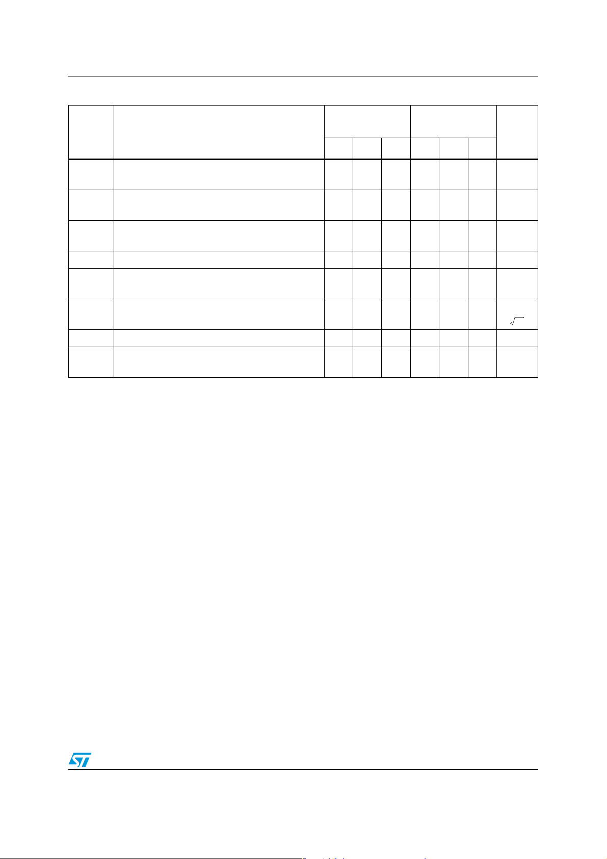
TL082 TL082A TL082B Absolute maximum ratings and operating conditions
2 Absolute maximum ratings and operating conditions
Table 1. Absolute maximum ratings
Symbol Parameter
V
V
V
P
Supply voltage
CC
Input voltage
in
Differential input voltage
id
Power dissipation 680 mW
tot
(1)
(2)
(3)
Thermal resistance junction to ambient
R
thja
SO-8
DIP8
TSSOP8
Thermal resistance junction to case
R
thjc
SO-8
DIP8
TSSOP8
Output short-circuit duration
T
ESD
Storage temperature range -65 to +150 °C
stg
HBM: human body model
MM: machine model
(6)
(7)
CDM: charged device model
(5)
(8)
(4)
TL082I, AI, BITL082C, AC,
BC
±18 V
±15 V
±30 V
125
85
120
40
41
37
Infinite
1kV
200 V
1500 V
Unit
°C/W
°C/W
1. All voltage values, except differential voltage, are with respect to the zero reference level (ground) of the
supply voltages where the zero reference level is the midpoint between V
2. The magnitude of the input voltage must never exceed the magnitude of the supply voltage or 15 volts,
whichever is less.
3. Differential voltages are the non-inverting input terminal with respect to the inverting input terminal.
4. Short-circuits can cause excessive heating. Destructive dissipation can result from simultaneous short-
circuit on all amplifiers.
5. The output may be shorted to ground or to either supply. Temperature and/or supply voltages must be
limited to ensure that the dissipation rating is not exceeded
6. Human body model: 100 pF discharged through a 1.5 kΩ resistor between two pins of the device, done for
all couples of pin combinations with other pins floating.
7. Machine model: a 200 pF cap is charged to the specified voltage, then discharged directly between two
pins of the device with no external series resistor (internal resistor < 5 Ω), done for all couples of pin
combinations with other pins floating.
8. Charged device model: all pins plus package are charged together to the specified voltage and then
discharged directly to the ground.
Table 2. Operating conditions
CC
+
and V
CC
-
.
Symbol Parameter TL082I, AI, BI TL082C, AC, BC Unit
V
T
oper
Supply voltage 6 to 36 V
CC
Operating free-air temperature range -40 to +105 0 to +70 °C
3/17
Electrical characteristics TL082 TL082A TL082B
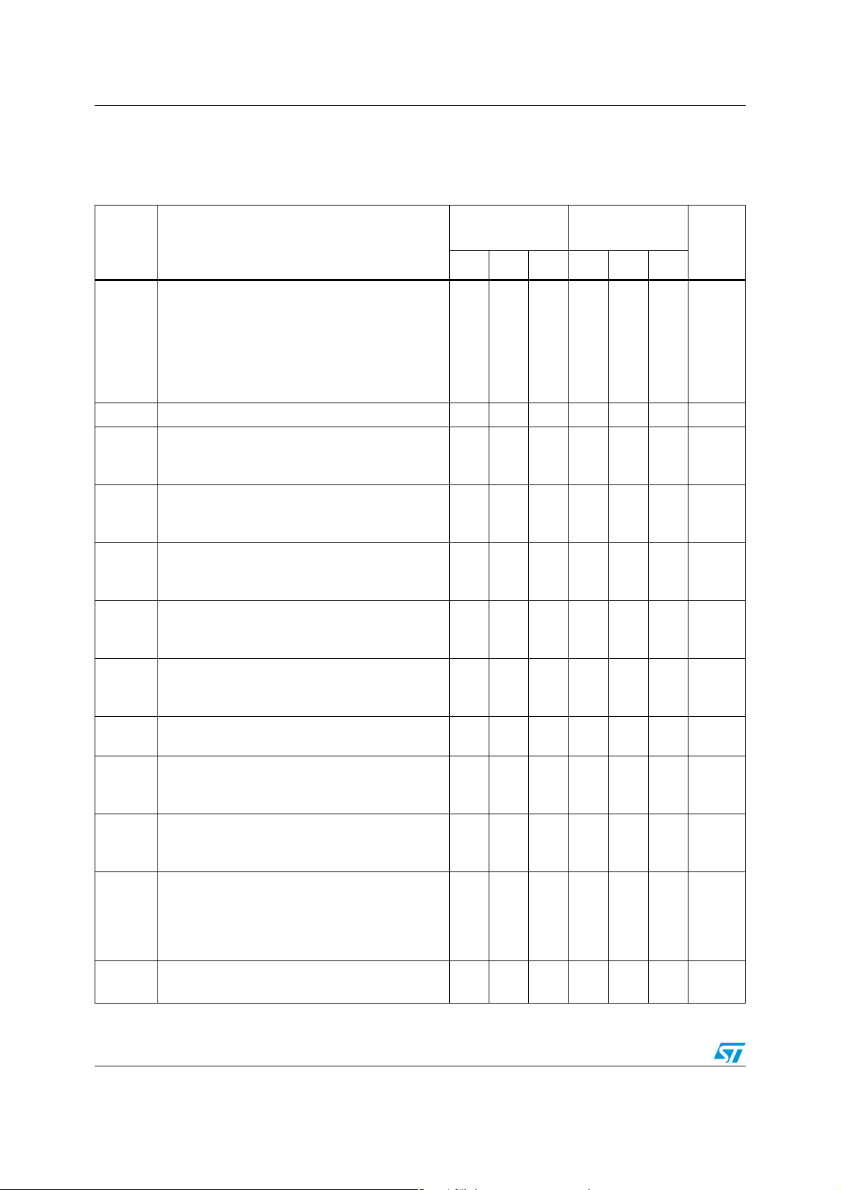
3 Electrical characteristics
Table 3. VCC = ±15V, T
= +25°C (unless otherwise specified)
amb
Symbol Parameter
Input offset voltage (Rs = 50Ω)
= +25°C TL082
T
amb
TL082A
V
io
T
≤ T
min
amb
≤ T
max
TL082B
TL082
TL082A
TL082B
DV
Input offset voltage drift 10 10 µV/°C
io
≤ T
max
(1)
Input offset current
I
io
T
T
amb
min
≤ T
= +25°C
amb
Input bias current
I
ib
T
T
amb
min
= +25°C
≤ T
amb
≤ T
max
Large signal voltage gain (RL = 2kΩ, Vo = ±10V)
A
vd
T
T
amb
min
= +25°C
≤ T
amb
≤ T
max
Supply voltage rejection ratio (R
SVR
T
T
amb
min
= +25°C
≤ T
amb
≤ T
max
Supply current, no load
I
CC
V
icm
T
= +25°C
amb
≤ T
T
min
amb
≤ T
max
Input common mode voltage range
= 50Ω)
S
TL082I,AC,AI,BC,
BI
TL082C
Min. Typ. Max. Min. Typ. Max.
3
10
3
6
1
3
13
310
13
7
5
5100
510010pA
4
20 200
20
20 400
20
5025200 2515200
808086 707086
1.4 2.5
±11 +15
-12
2.5
±11 +15
1.4 2.5
2.5
-12
Unit
mV
nA
pA
nA
V/mV
dB
mA
V
Common mode rejection ratio (RS = 50Ω)
CMR
T
T
amb
min
= +25°C
≤ T
amb
≤ T
max
Output short-circuit current
I
os
T
T
amb
min
= +25°C
≤ T
amb
≤ T
max
Output voltage swing
= +25°C RL = 2kΩ
T
T
amb
min
≤ T
amb
≤ T
RL = 10kΩ
RL = 2kΩ
max
±V
opp
RL = 10kΩ
SR
Slew rate
V
= 10V, RL = 2kΩ, CL = 100pF, unity gain 8 16 8 16 V/µs
in
4/17
808086 707086
101040 6060101040 60
60
10
12
10
12
12
13.5
10
12
10
12
12
13.5
dB
mA
V
TL082 TL082A TL082B Electrical characteristics
Table 3. VCC = ±15V, T
Symbol Parameter
= +25°C (unless otherwise specified) (continued)
amb
TL082I,AC,AI,BC,
BI
TL082C
Unit
Min. Typ. Max. Min. Typ. Max.
Rise time
t
r
K
ov
GBP
R
THD
e
n
i
Vin = 20mV, RL = 2kΩ, CL = 100pF, unity gain 0.1 0.1 µs
Overshoot
Vin = 20mV, RL = 2kΩ, CL = 100pF, unity gain 10 10 %
Gain bandwidth product
V
= 10mV, RL = 2kΩ, CL = 100pF, F= 100kHz 2.5 4 2.5 4 MHz
in
Input resistance 10
12
10
12
Total harmonic distortion
F=1kHz, R
= 2kΩ,CL=100pF, Av=20dB, Vo=2V
L
pp
0.01 0.01 %
Equivalent input noise voltage
= 100Ω, F = 1kHz 15 15
R
S
nV
------------
∅m Phase margin 45 45 degrees
Vo1/V
1. The input bias currents are junction leakage currents which approximately double for every 10° C increase in the junction
temperature.
Channel separation
o2
Av = 100
120 120 dB
Ω
Hz
5/17
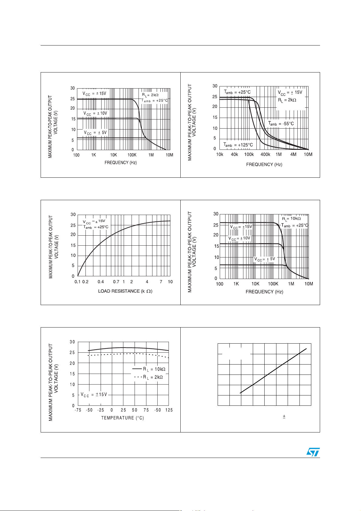
Electrical characteristics TL082 TL082A TL082B
30
25
20
15
10
5
02468101214 16
MAXIMUM PEAK-TO-PEAK OUTPUT
VOLTAG E (V)
R
L
= 10 k
Ω
T
amb
= +25˚C
SUPPLY VOLTAGE ( V)
Figure 2. Maximum peak-to-peak output
voltage versus frequency
Figure 4. Maximum peak-to-peak output
voltage versus load resistance
Figure 3. Maximum peak-to-peak output
voltage versus frequency
Figure 5. Maximum peak-to-peak output
voltage versus frequency
Figure 6. Maximum peak-to-peak output
6/17
voltage versus free air temperature
Figure 7. Maximum peak-to-peak output
voltage versus supply voltage

TL082 TL082A TL082B Electrical characteristics
0
5
1000
400
200
100
20
40
10
4
2
1
DIFFERENTIAL VOLTAGE
AMPLIFICATION (V/V)
-75 -50 -25 0
25 50 75
100
125
TEMPERATURE (˚C)
R
L
= 2k
Ω
V
O
= 10V
VCC= 15V
5
Figure 8. Input bias current versus free air
temperature
100
V
15V
=
CC
10
1
0.1
INPUT BIAS CURRENT (nA)
0.01
-50 -25 0 25 50 75 100 125
TEMPERATURE (˚C)
Figure 10. Supply current per amplifier versus
free air temperature
2.0
V
1.8
1.6
1.4
1.2
1.0
0.8
0.6
0.4
0.2
SUPPLY CURRENT (mA)
0
-75 -50 -25 0
50 75 100 12
25
TEMPERATURE (˚C)
=
CC
No signal
No load
15V
Figure 9. Large signal differential voltage
amplification and phase shift
versus frequency
100
PHASE SHIFT
(right scale)
10
R = 2k
C = 100pF
V = 15V
1
AMPLIFICATION (V/V)
DIFFERENTIAL VOLTAGE
T = +125°C
100
W
L
L
CC
amb
1K 10K 100K 10M1M
FREQUENCY (Hz)
DIFFERENTIAL
VOLTAGE
AMPLIFICATION
(left scale)
Figure 11. Large signal differential voltage
amplification versus free air temp.
180
9
0
Figure 12. Total power dissipation versus free
TOTAL POW ER DISSIPATION (mW)
air temperature
250
225
200
175
150
125
100
75
50
25
0
-75 -50 -25 0
50 75 100 12
25
TEMPERATURE (˚C)
V
=
CC
No signal
No load
15V
Figure 13. Supply current per amplifier versus
supply voltage
2.0
1.8
1.6
1.4
1.2
1.0
0.8
0.6
0.4
SUPPLY CURRENT (mA)
0.2
0
7/17
= +25˚C
T
amb
No signal
No load
246810 12 14 16
SUPPLY VOLTAGE ( V)

Electrical characteristics TL082 TL082A TL082B
5
70
60
50
40
30
20
10
0
EQUIVALENT INPUT NOISE
VOLTAGE (nV/VHz)
10 40 100 400 1k 4k 10k 40k 100k
FREQUENCY (Hz)
A
V
= 10
R
S
= 100
Ω
T
amb
= +25˚C
V
CC
= 15V
k
Figure 14. Common mode rejection ratio
versus free air temperature
89
R
= 10 k
Ω
L
88
V
= 15V
CC
87
86
85
RATIO (dB)
84
83
-50 -25 0 25 50 75 100 125
COMMON MODE MODE REJECTION
-75
TEMPERATURE (˚C)
Figure 16. Voltage follower large signal pulse
response
6
(V)
INPUT AND OUTPUT VOLTAGES
4
2
0
-2
-4
-6
0 0.5 1 1.5 2 2.5 3 3.
V
CC
R
L
C
= 100pF
L
T
amb
= 2 k
OUTPUT
= 15V
W
= +25°C
TIME (ms)
INPUT
Figure 15. Output voltage versus elapsed time
28
24
OVERSHOOT
20
90%
16
12
8
4
OUTPUT VOLTAGE (mV)
10%
0
-4
0
t
r
0.1 0.2
TIME (
0.3
V
= 15V
CC
R
= 2k
Ω
L
T
= +25˚C
amb
0.5
0.6
0.4
μ
s)
0.7
Figure 17. Equivalent input noise voltage
versus frequency
Figure 18. Total harmonic distortion versus
frequency
1
V
= 15V
V
= 15V
CC
0.4
0.1
0.04
(%)
0.01
0.004
0.001
TOTAL HARM ONIC DI STO RTION
8/17
CC
= 1
A
= 1
V
A
V
V
= 6V
V
= 6V
(rms)
O
(rms)
O
T
= +25˚C
= +25˚C
T
amb
amb
100 400 1k 4k 10k 40k 100
FREQUENCY (Hz)

TL082 TL082A TL082B Parameter measurement information
4 Parameter measurement information
Figure 19. Voltage follower
Figure 20. Gain-of-10 inverting amplifier
10k
Ω
1k
Ω
e
I
-
1/2
TL082
e
o
R
L
CL= 100pF
9/17

Typical applications TL082 TL082A TL082B
-
-
TL082
1/2
TL082
1/2
18pF
88.4k
Ω
18pF
88.4k
Ω
88.4k
Ω
18pF
1N 4148
1N 4148
18k Ω *
-15V
1k
Ω
1k
Ω
18k Ω *
+15V
6 cos ω t
6 sin
ω
t
5 Typical applications
Figure 21. 100 kHz quadruple oscillator
* These resistor values may be adjusted for a symmetrical output
10/17

TL082 TL082A TL082B Package information
6 Package information
In order to meet environmental requirements, STMicroelectronics offers these devices in
ECOPACK
category of second level interconnect is marked on the package and on the inner box label,
in compliance with JEDEC Standard JESD97. The maximum ratings related to soldering
conditions are also marked on the inner box label. ECOPACK is an STMicroelectronics
trademark. ECOPACK specifications are available at: www.st.com
®
packages. These packages have a lead-free second level interconnect. The
.
11/17

Package information TL082 TL082A TL082B
6.1 DIP8 package information
Figure 22. DIP8 package mechanical drawing
Table 4. DIP8 package mechanical data
Dimensions
Ref.
Min. Typ. Max. Min. Typ. Max.
A5.330.210
A1 0.38 0.015
A2 2.92 3.30 4.95 0.115 0.130 0.195
b 0.36 0.46 0.56 0.014 0.018 0.022
b2 1.14 1.52 1.78 0.045 0.060 0.070
c 0.20 0.25 0.36 0.008 0.010 0.014
D 9.02 9.27 10.16 0.355 0.365 0.400
E 7.62 7.87 8.26 0.300 0.310 0.325
E1 6.10 6.35 7.11 0.240 0.250 0.280
e 2.54 0.100
eA 7.62 0.300
eB 10.92 0.430
L 2.92 3.30 3.81 0.115 0.130 0.150
Millimeters Inches
12/17

TL082 TL082A TL082B Package information
6.2 SO-8 package information
Figure 23. SO-8 package mechanical drawing
Table 5. SO-8 package mechanical data
Dimensions
Ref.
Min. Typ. Max. Min. Typ. Max.
A1.750.069
A1 0.10 0.25 0.004 0.010
A2 1.25 0.049
b 0.28 0.48 0.011 0.019
c 0.17 0.23 0.007 0.010
D 4.80 4.90 5.00 0.189 0.193 0.197
E 5.80 6.00 6.20 0.228 0.236 0.244
E1 3.80 3.90 4.00 0.150 0.154 0.157
e 1.27 0.050
h 0.25 0.50 0.010 0.020
L 0.40 1.27 0.016 0.050
k1° 8°1° 8°
ccc 0.10 0.004
Millimeters Inches
13/17

Package information TL082 TL082A TL082B
6.3 TSSOP8 package information
Figure 24. TSSOP8 package mechanical drawing
Table 6. TSSOP8 package mechanical data
Dimensions
Ref.
Min. Typ. Max. Min. Typ. Max.
A 1.2 0.047
A1 0.05 0.15 0.002 0.006
A2 0.80 1.00 1.05 0.031 0.039 0.041
b 0.19 0.30 0.007 0.012
c 0.09 0.20 0.004 0.008
D 2.90 3.00 3.10 0.114 0.118 0.122
E 6.20 6.40 6.60 0.244 0.252 0.260
E1 4.30 4.40 4.50 0.169 0.173 0.177
e 0.65 0.0256
k0° 8°0° 8°
L 0.45 0.60 0.75 0.018 0.024 0.030
L1 1 0.039
aaa 0.1 0.004
Millimeters Inches
14/17

TL082 TL082A TL082B Ordering information
7 Ordering information
Table 7. Order codes
Order code Temperature range Package Packing Marking
TL082IN
TL082ID
TL082IDT
DIP8 Tube TL082IN
SO-8
Tub e o r
tape & reel
082I
TL082IPT TSSOP8 Tape & reel
TL082AIN DIP8 Tube TL082AIN
TL082AID
TL082AIDT
-40°C, +105°C
SO-8
Tub e o r
tape & reel
082AI
TL082AIPT TSSOP8 Tape & reel
TL082BIN DIP8 Tube TL082BIN
TL082BID
TL082BIDT
SO-8
Tub e o r
tape & reel
082BI
TL082BIPT TSSOP8 Tape & reel
TL082CN
TL082CD
TL082CDT
DIP8 Tube TL082CN
SO-8
Tub e o r
tape & reel
082C
TL082CPT TSSOP8 Tape & reel
TL082ACN DIP8 Tube TL082ACN
TL082ACD
TL082ACDT
0°C, +70°C
SO-8
Tub e o r
tape & reel
082AC
TL082ACPT TSSOP8 Tape & reel
TL082BCN DIP8 Tube TL082BCN
TL082BCD
TL082BCDT
SO-8
Tub e o r
tape & reel
082BC
TL082BCPT TSSOP8 Tape & reel
TL082IYDT
TL082AIYDT
TL082BIYDT
(1)
(1)
(1)
-40°C, +105°C
SO8
(automotive grade)
Tub e o r
tape & reel
082IY
82AIY
82BIY
1. Qualified and characterized according to AEC Q100 and Q003 or equivalent, advanced screening
according to AEC Q001 & Q 002 or equivalent.
15/17

Revision history TL082 TL082A TL082B
8 Revision history
Table 8. Document revision history
Date Revision Changes
02-Apr-2001 1 Initial release.
2002-2003 2-7 Internal revisions.
30-Apr-2004 8 Format update.
Added ESD information in Table 1 on page 3.
Expanded order codes table and added automotive grade order
06-Mar-2007 9
17-Jun-2008 10
codes. See Table 7 on page 15.
Added Table 2: Operating conditions on page 3.
Updated package information to make it compliant with the latest
JEDEC standards.
Removed information concerning military temperature range
(TL082M*, TL082AM*, TL082BM*).
16/17

TL082 TL082A TL082B
Please Read Carefully:
Information in this document is provided solely in connection with ST products. STMicroelectronics NV and its subsidiaries (“ST”) reserve the
right to make changes, corrections, modifications or improvements, to this document, and the products and services described herein at any
time, without notice.
All ST products are sold pursuant to ST’s terms and conditions of sale.
Purchasers are solely responsible for the choice, selection and use of the ST products and services described herein, and ST assumes no
liability whatsoever relating to the choice, selection or use of the ST products and services described herein.
No license, express or implied, by estoppel or otherwise, to any intellectual property rights is granted under this document. If any part of this
document refers to any third party products or services it shall not be deemed a license grant by ST for the use of such third party products
or services, or any intellectual property contained therein or considered as a warranty covering the use in any manner whatsoever of such
third party products or services or any intellectual property contained therein.
UNLESS OTHERWISE SET FORTH IN ST’S TERMS AND CONDITIONS OF SALE ST DISCLAIMS ANY EXPRESS OR IMPLIED
WARRANTY WITH RESPECT TO THE USE AND/OR SALE OF ST PRODUCTS INCLUDING WITHOUT LIMITATION IMPLIED
WARRANTIES OF MERCHANTABILITY, FITNESS FOR A PARTICULAR PURPOSE (AND THEIR EQUIVALENTS UNDER THE LAWS
OF ANY JURISDICTION), OR INFRINGEMENT OF ANY PATENT, COPYRIGHT OR OTHER INTELLECTUAL PROPERTY RIGHT.
UNLESS EXPRESSLY APPROVED IN WRITING BY AN AUTHORIZED ST REPRESENTATIVE, ST PRODUCTS ARE NOT
RECOMMENDED, AUTHORIZED OR WARRANTED FOR USE IN MILITARY, AIR CRAFT, SPACE, LIFE SAVING, OR LIFE SUSTAINING
APPLICATIONS, NOR IN PRODUCTS OR SYSTEMS WHERE FAILURE OR MALFUNCTION MAY RESULT IN PERSONAL INJURY,
DEATH, OR SEVERE PROPERTY OR ENVIRONMENTAL DAMAGE. ST PRODUCTS WHICH ARE NOT SPECIFIED AS "AUTOMOTIVE
GRADE" MAY ONLY BE USED IN AUTOMOTIVE APPLICATIONS AT USER’S OWN RISK.
Resale of ST products with provisions different from the statements and/or technical features set forth in this document shall immediately void
any warranty granted by ST for the ST product or service described herein and shall not create or extend in any manner whatsoever, any
liability of ST.
ST and the ST logo are trademarks or registered trademarks of ST in various countries.
Information in this document supersedes and replaces all information previously supplied.
The ST logo is a registered trademark of STMicroelectronics. All other names are the property of their respective owners.
© 2008 STMicroelectronics - All rights reserved
STMicroelectronics group of companies
Australia - Belgium - Brazil - Canada - China - Czech Republic - Finland - France - Germany - Hong Kong - India - Israel - Italy - Japan -
Malaysia - Malta - Morocco - Singapore - Spain - Sweden - Switzerland - United Kingdom - United States of America
www.st.com
17/17
 Loading...